Defect engineering of the electronic transport through cuprous oxide interlayers
Abstract
The electronic transport through Au–(Cu2O)n–Au junctions is investigated using first-principles calculations and the nonequilibrium Green’s function method. The effect of varying the thickness (i.e., ) is studied as well as that of point defects and anion substitution. For all Cu2O thicknesses the conductance is more enhanced by bulk-like (in contrast to near-interface) defects, with the exception of O vacancies and Cl substitutional defects. A similar transmission behavior results from Cu deficiency and N substitution, as well as from Cl substitution and N interstitials for thick Cu2O junctions. In agreement with recent experimental observations, it is found that N and Cl doping enhances the conductance. A Frenkel defect, i.e., a superposition of an O interstitial and O substitutional defect, leads to a remarkably high conductance. From the analysis of the defect formation energies, Cu vacancies are found to be particularly stable, in agreement with earlier experimental and theoretical work.
pacs:
73.20.-r, 73.40.RwLow production costs and the right band gap are key factors for applications of p-type semiconductors. Cuprous oxide (Cu2O) fulfils both criteria, making the material interesting for optoelectronic devices Zakutayev , coatings Nguyen , sensors Deng , etc. It has a simple cubic structure with lattice constant Å and a direct band gap at the center of the Brillouin zone, experimentally given by eV; see Ref. 4 for a recent review. From the theoretical point of view, Hartree-Fock and semi-empirical extended Hückel methods have been used for describing the electronic structure, resulting in massive overestimations of the band gap Ruiz ; Buljan . On the other hand, density functional theory underestimates the gap, giving 0.5 to 0.7 eV within the local density approximation (LDA) Buljan ; Heinemann , eV using the LDA+U approach Heinemann , and eV using the self-interaction correction method Filippetti . The Heyd-Scuseria-Ernzerhof (HSE06) hybrid functional gives a band gap of eV, close to the experimental value Heinemann . All the above mentioned first-principles approaches find the valence band maximum to be dominated by Cu states, and the conduction band minimum by Cu states, though hybridization is important for the material properties Ruiz ; Buljan ; Nolan .
Vacancies and interstitial defects in Cu2O have been studied experimentally for many years, for example, O and Cu vacancies as well as Cu interstitials in Refs. 10; 11; 12; 13; 14; 15. The effect of doping with nonmetallic anions at the O site has been investigated for Cl Musa and N Ish1 ; Li ; when doping with Si, Cu vacancy sites are preferably occupied Ish2 ; Nemoto . Cation doping at the Cu site has been reported for various metals, including Be Keeffe , Mn Wei , Co Kale , Ni Kik1 ; Kik2 , Ag Tseng , and Cd Pap1 ; Pap2 . As concerns the theoretical methods, the generalized gradient approximation (GGA) has been employed to investigate the effects of O and Cu vacancies, anti-sites, and interstitials Nolan ; Soon . The GGA+U approach has been used to study the effects of Mn, Fe, Co, and Ni substitutional doping on the electronic and magnetic properties, indicating the possibility of long-range ferromagnetism when O and Cu vacancies are introduced Sieberer . GGA calculations also have been reported for doping with the transition metals Ag, Ni, and Zn Martinez . Ag substitutional doping turns out to reduce only the band gap, whereas Zn doping leads to n-type conduction.
Since the performance of a device usually is dominated by interface properties Liu ; Zhang , Cu/Cu2O and Au/Cu2O interfaces have been addressed in Refs. 34 and 32, respectively. In particular, In2S3/Cu2O Jaya and ZnO/Cu2O Yang interfaces have been found to be promising for photovoltaic applications. From the experimental point of view, the electrical resistivities of a Cu2O thin film between two gold leads using SiO2/Si substrates Ra , and of a sulfur-treated n-type Cu2O thin film with Ag, Cu, Au, or Ni front contacts have been measured Rb . However, very little is known about the theoretical understanding of electronic transport properties of heterojunctions involving Cu2O.
In order to provide insight into this question, we study in the following prototypical Au–(Cu2O)n–Au junctions including different kinds of defects such as vacancies (O or Cu), substitutional, interstitial (N or Cl) and Frenkel defects at different positions in the structures. We carefully optimize the atomic positions, in order to obtain physically relevant results. Note that in the main text our focus is on the optimized structures; but in most figures we include also the results for the unrelaxed structures for comparison, including some brief comments in order to highlight relevant changes due to relaxation. As is apparent from the results, the optimization of the structures strongly affects the electronic structure and transport properties such as the transmission coefficient and the conductance. Generally bulk defects are more effective for enhancing transport than near-interface defects. In order to increase the conductance we suggest that interstitial defects are more suitable than substitutional ones.
We note from the start that formally, one defect for the junction corresponds to a defect concentration of 3.8 %. We also wish to emphasize that the comparison of our model results with experimental data can only be qualitatitive, since the latter strongly depend on the method of preparation, as well as the concrete substrate—which we are, at least at present, not able to incorporate in a quantitative way.
Results
Using SIESTA Sol as electronic structure package, the transport properties are calculated by the SMEAGOL Rocha1 ; Rocha2 ; Rungger code, which employs the nonequilibrium Green’s functions method. Periodic boundary conditions are applied perpendicular to the [100] transport direction. The Perdew-Burke-Ernzerhof version Perdew of the GGA is utilized for the exchange-correlation potential. Moreover, the energy cutoff is set to 250 Ry, and Monkhorst-Pack k-meshes of points for the leads and points for the transport calculations are used. Norm-conserving pseudopotentials are employed (fully nonlocal Kleinman-Bylander type Kleinman with double-zeta basis set). The pseudopotentials for the Cu, O and Cl atoms include nonlinear core corrections in the exchange correlation potential Louie . The basis set superposition error is corrected using the counterpoise procedure Boys .
A lattice strain of 4 % is introduced by assuming an epitaxial interface, and therefore setting the Cu2O lattice constant to the Au value of 4.09 Å. All structural optimizations (relaxations) are based on the conjugate gradient method, converging the net force on each atom down to 0.04 eV/Å. The leads are modeled by two atomic layers of face centered cubic [001] Au; in addition, four Au layers on each side of the (Cu2O)n layer are included in the scattering region. We study Au–(Cu2O)n–Au junctions comprising to 4 Cu2O unit cells, which corresponds to 3 to 9 atomic layers of Cu2O.
Comparison to previously published theoretical results on bulk Cu2O and Au shows good agreement with our calculations for the bulk materials Heinemann . The well-known fact that GGA underestimates the bulk band gap indeed is an issue of debate, but we take here the point of view that, since the band dispersions are qualitatively correctly described by first-principles calculations, a correct description of transport through small heterostructures can be expected, in particular, concerning the defect and doping dependence.
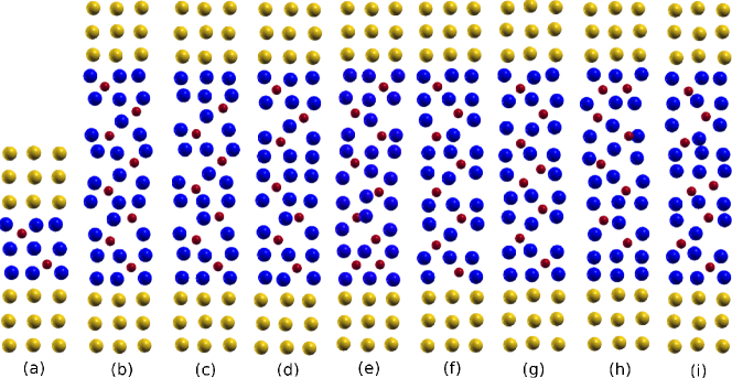
The pristine and defective heterojunctions under study are displayed in Fig. 1. We consider, in particular, defects at or near the interface (near-interface), as well as in the bulk (bulk-like). Concerning O, we study O vacancies near-interface, Fig. 1(c), and bulk-like, Fig. 1(d), and O interstitials near-interface, Fig. 1(e), and in the bulk (not presented in Fig. 1). Furthermore, Cu vacanies at the interface, Fig. 1(f), and in the bulk, Fig. 1(g), are addressed. For Frenkel defects, where an O atom is removed from a certain layer and inserted into another one, there are two possibilities, near-interface, Fig. 1(h), and bulk-like, Fig. 1(i). Finally, N and Cl substitutional and interstitial defects are also considered at different postions in the structure.
Due to the contact between Au and Cu2O, the optimization changes the positions of the atoms at the interface and in the bulk of the Cu2O interlayer; for pristine junctions, e.g., the Au–Cu distance at the interface is reduced by about 4 % due to relaxation. Defects, even those that are two layers away from the interface, alter the atomic positions further: in fact the additional shift of Cu towards Au at the interface is maximal for the cases (e), (g), and (h) in Fig. 1 (another 6 %).
The defect formation energies give an indication which defects are more likely to be of experimental relevance than others; it is defined as the energy of the defective structure, minus the energy of the respective “constituents”:
| (1) |
where the subscript “total” refers to the respective total energies. For example, for an X vacancy, is given by the total energy of the pristine structure, from which the energy of a single X atom is subtracted:
| (2) |
easy In particular, we determine from the Cu bulk energy, while we assume to be half the molecular energy. For a substitutional defect, where the atom X is replaced by the atom Y, we have
| (3) |
The argumentation for interstitial and Frenkel defects proceeds similarly.
The formation energies—as well as the respective conductances, to be discussed below—are given in Table I. It is apparent that O interstitials are by far the most stable defects among the ones considered, followed by Cu vacancy bulk-like, N interstitial bulk-like, and bulk-like Frenkel defects. Generally bulk-like defects are more favorable than interfacial ones except for O vacancies, N interstitial and Cl substitutional defects. The stability of structures with Cu vacancies observed here was noticed in previous theoretical studies Raebiger ; Scanlon1 ; Scanlon2 , and was also seen experimentally Jongh ; Garuthara ; Zouaghi ; Fujinaka .
.1 Pristine junction
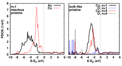
The projected density of states (PDOS) of the interfacial atoms for the pristine Au–Cu2O–Au heterojunction is shown in Fig. 2 (left). Broad Cu and Au states are apparent, as well as signs of Cu–Au hybridization, particularly at eV. Figure 2 (right) refers to the bulk-like O and Cu atoms in the center of the Cu2O region for and . The enhanced Cu–O hybridization around eV is characteristic for the case. Down to about eV we observe the expected dominance of Cu states, the DOS structure being broader for .
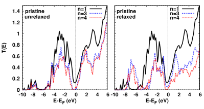
The transmission coefficients and thickness () dependencies are shown in Fig. 3. For the optimized structure (right), reflects the shape of the DOS below the Fermi energy, , compare Fig. 2: most notable are the peak near eV (due to the localized Cu levels), as well as the almost constant DOS above (due to the extended Cu states). We expect that the transmission at is dominated by Cu states, since Cu is located next to Au in the junctions studied. The corresponding conductance, , is of the order of (for ), where denotes the conductance quantum (the factor 2 is due to the spin). Increasing to 4, the conductance drops to .
Above , increases roughly linearly with energy due to the delocalized Cu 4s states. The transmission decreases with increasing thickness . A transport gap of approximately 0.6 eV appears for the relaxed structure when increasing to 4. For any thickness studied the heterojunction behaves as an n-type conductor. In the following, we omit the results for since they are similar to those for .
.2 O and Cu defects
First we discuss the role of O and Cu vacancies and O interstitial defects, cf. Fig. 1, (c)–(g), as well as of Frenkel defects, which consist of an O vacancy and an O interstitial, cf. Fig. 1, (h) and (i).
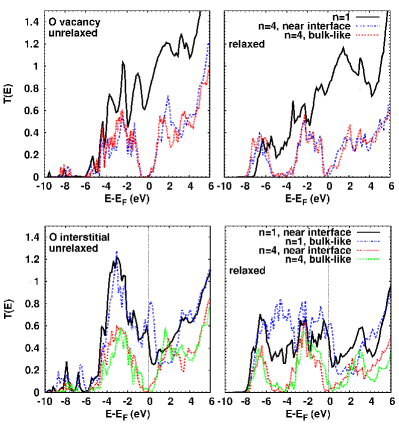
Figure 4 shows for O vacancies (top part of the figure) and O interstitial defects (bottom part of the figure). In the following, we concentrate our discussion on the optimized structures (right). A major change of the transmission, compared to the pristine junction, is observable for both cases for , namely a shift of weight from the peak around eV towards , and an enhancement below eV. However, is more evenly distributed for an interstitial defect. In addition, is enhanced at the Fermi energy by vacancies due to contributions from Au and Cu states, as is apparent from the respective PDOS (not shown here). The conductance is , and thus considerably larger than in the pristine case.
For the thicker Cu2O layer, , we consider O vacancies at the interface and in the center of the Cu2O region, see Fig. 1, (c) and (d). The exact position of the vacancy plays only a minor role for . As compared to the pristine junction, the transport gap at has closed, but the conductance is rather small, about and for the near-interface and bulk-like vacancy, respectively.
An O interstitial atom in a thin () Cu2O interlayer results in a significant down to eV, see Fig. 4 (rightmost). Furthermore, the minimum of around is completely washed out, resulting in enhanced conductances of (near-interface) and (bulk-like). However, the enhancement is slightly less than what is observed for O vacancies. For the thick () Cu2O layer the effect of an interstitial O atom strongly depends on its position: the conductance is considerably higher for the bulk-like than for the near-interface interstitial ( vs. ). This fact can be related to a strong contribution of p orbitals, which lead to a clearly visible peak in the O (bulk-like) PDOS at , even larger than the Cu (bulk-like) PDOS. For a near-interface interstitial, on the other hand, this peak is located near eV. Overall behaves similar to the pristine junction.
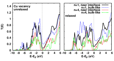
In Fig. 5 we show the transmission coefficients for Cu vacancies; we focus again the discussion on the optimized structures (right). As compared to the pristine junction, vacancies enhance below eV for . For an interfacial Cu vacancy the change in below can be related to the sensitivity of the bands to disorder, and the Au()–Cu() orbital interaction at the interface Autes . The conductance is reduced (compared to the pristine junction) to (). For a bulk-like Cu vacancy an enhanced is visible between and eV due to contributions from Cu 3d bulk states, and the conductance is given by . An increase of the conductance due to Cu vacancies is in agreement with previous work on thin films Isseroff . Independent of its position, a Cu vacancy shifts the minimum of around to higher energy.
On the other hand, for a thick () Cu2O layer, the gross shape of for Cu vacancies is very similar to the case of O vacancies. The conductance, however, is higher for the bulk-like than for the interfacial Cu vacancy ( vs. ). Note that the conduction type can be modified by Cu vacancies.
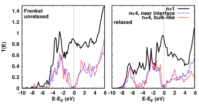
Turning to Fig. 6, we observe that a Frenkel defect modifies substantially for , leading to a very high conductance of . For we consider the two Frenkel defect configurations shown in Fig. 1, (h) and (i). We find no significant difference in , and obtain essentially the same conductance (0.070 vs. ) for both of them. Roughly speaking, can be considered a combination of the effects of an O vacancy and an O interstitial.
.3 N and Cl doping
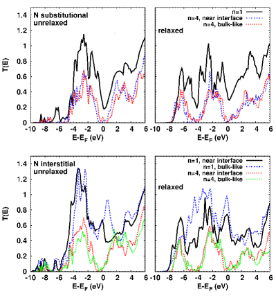
The effect of N substitutional and interstitial doping is addressed in Fig. 7. Clearly the onset of is related to the energetic positions of the N relative to the Cu states, and the high around eV is due to a strong overlap between them. Minima in , for example near eV, coincide with minima in the Cu PDOS (not shown here). The shift of the minimum of around to higher energy is similar to the effect of a Cu vacancy. Conductance values of , , and are obtained for N substitution, near-interface N interstitial, and bulk-like N interstitial, respectively (). Substitution creates an excess hole, while an interstitial defect creates excess electrons. This explains why the conductance is higher for the interstitial than for the substitutional case. For bulk-like N interstitial there are more transmission channels than for the near-interface N interstitial at .
Figure 7 also deals with N doping at different positions for . Comparing substitutional and interstitial doping, the overall energy dependence is quite similar (and similar to the pristine junction), except for subtle differences near . As compared to the pristine junction, the transport gap is slightly reduced, and the conductance thus a little enhanced, similarly for bulk-like and near-interface substitution, to about . Turning to N interstitial defects (), Fig. 7 shows that the bulk-like position of the defect results in a slightly higher conductance than the near-interface position, vs. .
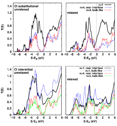
Figure 8 addresses Cl doping. For substitutional doping, we find close similarities to the pristine junction though the minimum near has shifted to lower energy, which is opposite to what is found for N doping. The conductance of about accordingly is higher than in the pristine junction, but lower than in the case of N doping. The shift of the minimum of to lower energy appears also for the Cl interstitial defect. A bulk-like Cl interstitial defect leads to a higher conductance () than a near-interface Cl interstitial defect ().
Interestingly, see Fig. 8, for we find again a shift of the minimum of near to higher energy (compared to the pristine case) for the bulk-like Cl substitutional defect. The conductances are given by and for near-interface and bulk-like substitution, respectively, which is considerably higher than for N substitution. In contrast to the other cases considered, the Cl bulk-like substitution has a lower conductance than the near-interafce one. The overall results for Cl interstitials are similar to those for N interstitial defects, but with slightly smaller conductances ( for the near-interface, and for the bulk-like case). The calculated conductances for are summarized in Table I.
Discussion
Based on the density functional theory and the nonequilibrium Green’s function approach, a comprehensive study of the electronic structure and transport properties of Au–(Cu2O)n–Au heterojunctions of different thickness, with different point defects, and with different kinds of anion doping of Cu2O has been carried out. As to be expected, the transmission decreases with inceasing . Compared to the pristine junction, we find for thin interlayers, , for O vacancies and for interstitial O, N, and Cl defects a drastic change of around the Fermi energy. Bulk-like defects are found to enhance the transport more effectively than near-interface defects—which appears reasonable since the system has a better chance to adjust to a bulk-like compared to a near-interface disturbance, thereby reducing scattering. Accordingly, we also find that for all cases considered the formation energy is lower for bulk-like than for interface or near-interface disturbances.
Experimentally it has been found that N and Cl doping enhances the conductance Musa ; Ish1 , and that interstitial N defects are more effective than N substitution Li . While this agrees with our findings, further work is needed to establish the connection between the present model studies and the actual experimental situation, where, in particular, the film thicknesses are much larger than the ones in our model. Note that for Cl we observe the opposite trend: interstitial defects are less effective than substitution. In conclusion, our investigation provides indications on how to improve the electrical and photovoltaic properties of Cu2O contacted by two gold leads, namely by appropriate, preferably bulk-like defect engineering. Of course, it must be kept in mind that the detailed experimental conditions may not always be properly reflected by the idealized theoretical modelling.
Acknowledgements.
We acknowledge financial support by the Deutsche Forschungsgemeinschaft (through TRR 80). Research reported in this publication was supported by the King Abdullah University of Science and Technology (KAUST).Author contributions
M.M.F. performed the calculations. All authors contributed to the analysis of the results and the writing of the manuscript.
Additional information
The authors declare no competing financial interests.
| G | O | G | N | G | Cl | G | |||||
|---|---|---|---|---|---|---|---|---|---|---|---|
| O vacancy, | interst., | interst., | interst., | ||||||||
| near interf. | 0.3 | 5.8 | near interf. | 0.2 | 2.0 | near interf. | 0.1 | 3.1 | near interf. | 0.1 | 2.2 |
| O vacancy, | interst., | interst., | interst., | ||||||||
| bulk-like | 0.4 | 3.2 | bulk-like | 1.7 | 11 | bulk-like | 1.1 | 6.1 | bulk-like | 0.2 | 3.3 |
| Cu vacancy, | Frenkel, | subst., | subst., | ||||||||
| at interf. | 0.3 | 2.6 | near interf. | 0.8 | 7.0 | near interf. | 2.0 | 1.5 | near interf. | 1.1 | 6.5 |
| Cu vacancy, | Frenkel, | subst., | subst., | ||||||||
| bulk-like | 1.6 | 3.2 | bulk-like | 0.8 | 7.5 | bulk-like | 1.0 | 1.4 | bulk-like | 1.9 | 4.3 |
References
- (1) Zakutayev, A., Stevanovic, V. & Lany, S. Non-equilibrium Alloying controls optoelectronic properties in Cu2O thin films for photovoltaic absorber applications. Appl. Phys. Lett. 106, 123903 (2015).
- (2) Nguyen, S. H., Lim, J.-C. & Lee, J.-K. Improving the performance of silicon anode in lithium-ion batteries by Cu2O coating layer. J. Appl. Electrochem. 44, 353–360 (2014).
- (3) Deng, S. et al. Reduced Graphene oxide conjugated Cu2O nanowire mesocrystals for high-performance NO2 gas sensor. J. Am. Chem. Soc. 134, 4905–4917 (2012) .
- (4) Meyer, B. K. et al. Binary Copper oxide semiconductors: From materials towards devices. Phys. Status Solidi B 249, 1487–1509 (2012).
- (5) Ruiz, E., Alvarez, S., Alemany, P. & Evarestov, R. A. Electronic Structure and properties of Cu2O. Phys. Rev. B 56, 7189–7196 (1997).
- (6) Buljan, A., Llunell, M., Ruiz, E. & Alemany, P. Color and conductivity in Cu2O and CuAlO2: A theoretical analysis of d interactions in solid-state compounds. Chem. Mater. 13, 338–344 (2001).
- (7) Heinemann, M., Eifert, B. & Heiliger, C. Band structure and phase stability of the copper oxides Cu2O, CuO, and Cu4O3. Phys. Rev. B 87, 115111 (2013).
- (8) Filippetti, A. & Fiorentini, V. Coexistence of ionic and metallic bonding in noble-metal oxides. Phys. Rev. B 72, 035128 (2005).
- (9) Nolan, M. & Elliott, S. D. The p-Type conduction mechanism in Cu2O: A first principles study. Phys. Chem. Chem. Phys. 8, 5350–5358 (2006).
- (10) Yoshimura, M., Revcolevschi, A. & Castaing, J. Thermogravimetric study of the non-stoichiometry of cuprite Cu2O. J. Mater. Sci. 11, 384–386 (1976).
- (11) Xue, J. & Dieckmann, R. The non-stoichiometry and the point defect structure of cuprous oxide (Cu2-δO). J. Phys. Chem. Solids 51, 1263–1275 (1990).
- (12) Porat, O. & I. Riess, I. Defect chemistry of Cu2-yO at elevated temperatures. part i: Non-stoichiometry, phase width and dominant point defects. Solid State Ionics 74, 229–238 (1994).
- (13) Aggarwal, S., Topfer, J., Tsai, T. L. & Dieckmann, R. Point defects and transport in binary and ternary, non-stoichiometric oxides. Solid State Ionics 101, 321–331 (1997).
- (14) Kim, J. Y., Rodriguez, J. A., Hanson, J. C., Frenkel, A. I. & Lee, P. L. Reduction of CuO and Cu2O with H2: H embedding and kinetic effects in the formation of suboxides. J. Am. Chem. Soc. 125, 10684–10692 (2003).
- (15) Isseroff, L. Y. & Carter, E. A. Electronic structure of pure and doped cuprous oxide with copper vacancies: Suppression of trap states. Chem. Mater. 25, 253–265 (2013).
- (16) Musa, A. O., Akomolafe, T. & Carter, M. J. Production of cuprous oxide, a solar cell material, by thermal oxidation and a study of its physical and electrical properties. Sol. Energy Mater. Sol. Cells 51, 305–316 (1998).
- (17) Ishizuka, S., Kato, S., Okamto, Y. & Akimoto, K. Nitrogen doping into Cu2O thin films deposited by reactive radio-frequency magnetron sputtering. Jpn. J. Appl. Phys. 40, 2765–2768 (2001).
- (18) Li, J. et al. Probing defects in nitrogen-doped Cu2O. Sci. Rep. 4, 7240 (2014).
- (19) Ishizuka, S., Kato, S., Maruyama, T. & Akimoto, K. Control of hole carrier density of polycrystalline Cu2O thin films by Si doping. Appl. Phys. Lett. 80, 950–952 (2002).
- (20) Nemoto, T. & Nakano, T. The effect of silicon on cuprous oxide. Jpn. J. Appl. Phys. 6, 543–544 (1967).
- (21) O’Keeffe, M. & Moore, W. J. Electrical conductivity of monocrystalline cuprous oxide. J. Chem. Phys. 35, 1324–1328 (1961).
- (22) Wei, M. et al. Room temperature ferromagnetism in bulk Mn-doped Cu2O. Appl. Phys. Lett. 86, 072514 (2005).
- (23) Kale, S. et al. Magnetism in cobalt-doped Cu2O thin films without and with Al, V, or Zn codopants. App. Phys. Lett. 82, 2100–2102 (2003).
- (24) Kikuchi, N. & Tonooka, K. Electrical and structural properties of Ni-doped Cu2O films prepared by pulsed laser deposition. Thin Solid Films 486, 33–37 (2005).
- (25) Kikuchi, N., Tonooka, K. & Kusano, E. Mechanisms of carrier generation and transport in Ni-doped Cu2O. Vacuum 80, 756–760 (2006).
- (26) Tseng, C. C., Hsieh, J. H., Liu, S. J. & Wu. W. Effects of Ag contents and deposition temperatures on the electrical and optical behaviors of Ag-doped Cu2O thin films. Thin Solid Films 518, 1407–1410 (2009).
- (27) Papadimitriou, L., Dimitriadis, C. A., Dozsa, L. & Andor, L. Acceptor states distributed in energy in Cd-doped Cu2O. Solid State Commun. 71, 181–185 (1989).
- (28) Papadimitriou, L. DLTS evaluation of nonexponential transients of defect levels in cuprous oxide (Cu2O). Solid-State Electron. 36, 431–434 (1993).
- (29) Soon, A., Cui, X. Y., Delley, B., Wei, S. H. & Stampfl, C. Native defect-induced multifarious magnetism in nonstoichiometric cuprous oxide: First-principles study of bulk and surface properties of Cu2-δO. Phys. Rev. B 79, 035205 (2009).
- (30) Sieberer, M., Redinger, J. & Mohn, P. Electronic and magnetic structure of cuprous oxide Cu2O doped with Mn, Fe, Co, and Ni: A density-functional theory study. Phys. Rev. B 75, 035203 (2007).
- (31) Martinez-Ruiz, A., Moreno, M. G. & Takeuchi, N. First principles calculations of the electronic properties of bulk Cu2O, clean and doped with Ag, Ni, and Zn. Solid State Sci. 5, 291–295 (2003).
- (32) Liu, D., Zhu, Y. F. & Jiang, Q. DFT study of CO oxidation on Cu2O-Au interfaces at Au-Cu alloy surfaces. RSC Adv. 5, 1587–1597 (2015).
- (33) Zhang, L., Kim, H. Y. & Henkelman, G. CO oxidation at the Au-Cu interface of bimetallic nanoclusters supported on CeO2(111). J. Phys. Chem. Lett. 4, 2943–2947 (2013).
- (34) Blajiev, O. L. & Hubin, A. The effect of silicon on cuprous oxide. Electrochim. Acta 50, 4297–4307 (2005).
- (35) Jayakrishnan, R. Photovoltaic response of Cu2O/In2S3 hetero-structure grown on Cu substrate. Mater. Sci. Semicond. Process. 16, 1608–1612 (2013).
- (36) Yang, M., Zhu, L., Li, Y., Cao, L. & Guo, Y. Asymmetric interface band alignments of Cu2O/ZnO and ZnO/Cu2O heterojunctions. J. Alloys Comp. 578, 143–147 (2013).
- (37) De Los Santos Valladares L. et al. Crystallization and electrical resistivity of Cu2O and CuO obtained by thermal oxidation of Cu thin films on SiO2/Si substrates. Thin Solid Films 520, 6368–6374 (2012).
- (38) Jayathilaka, K. M. D. C., Kapaklis, V., Siripala, W. & Jayanetti, J. K. D. S. Surface treatment of electrodeposited n-type Cu2O thin films for applications in Cu2O based devices. Phys. Status Solidi RRL 8, 592–595 (2014).
- (39) Soler, J. M. et al. Ab initio derivation of the electronic structure properties across the Cu-Cu2O interface. J. Phys.: Condens. Matter 14, 2745–2779 (2002).
- (40) Rocha, A. R. et al. Towards molecular spintronics. Nature Mater. 4, 335–339 (2005).
- (41) Rocha, A. R. et al. Spin and molecular electronics in atomically generated orbital landscapes. Phys. Rev. B 73, 085414 (2006).
- (42) Rungger, I. & Sanvito, S. Algorithm for the construction of self-energies for electronic transport calculations based on singularity elimination and singular value decomposition. Phys. Rev. B 78, 035407 (2008).
- (43) Perdew, J. P., Burke, K. & Ernzerhof, M. Generalized gradient approximation made simple. Phys. Rev. Lett. 77, 3865–3868 (1996).
- (44) Kleinman, L. & Bylander, D. M. Efficacious form for model pseudopotentials. Phys. Rev. Lett. 48, 1425–1428 (1982).
- (45) Louie, S. G., Froyen, S. & Cohen, M. L. Nonlinear ionic pseudopotentials in spin-density-functional calculations. Phys. Rev. B 26, 1738–1742 (1982).
- (46) Boys, S. F. & Bernardi, F. The calculation of small molecular interactions by the differences of separate total energies. Some procedures with reduced errors. Mol. Phys. 19, 553 (1970).
- (47) Raebiger, H., Lany, S. & Zunger, A. Origins of the p-type nature and cation deficiency in Cu2O and related materials. Phys. Rev. B 76, 045209 (2007).
- (48) Scanlon, D. O., Morgan, B. J. & Watson, G. W. Modeling the polaronic nature of p-type defects in Cu2O: The failure of GGA and GGA+U. J. Chem. Phys. 131, 124703 (2009).
- (49) Scanlon, D. O., Morgan, B. J., Watson, G. W. & Walsh, A. Acceptor levels in p-type Cu2O: Rationalizing theory and experiment. Phys. Rev. Lett. 103, 096405 (2009).
- (50) De Jongh, P. E., Vanmaekelbergh, D. & Kelly, J. J. Photoelectrochemistry of electrodeposited Cu2O. J. Electrochem. Soc. 147, 486–489 (2000).
- (51) Garuthara, R. & Siripala, W. Photoluminescence characterization of polycrystalline n-type Cu2O films. J. Lumin. 121, 173–178 (2006).
- (52) Zouaghi, M., Tapiero, M., Zielinger, J. P. & Burgraf, R. Hall mobility and hole density in photoactivated Cu2O single crystals. Solid State Commun. 8, 1823–1825 (1970).
- (53) Fujinaka, M. & Berezin, A. A. Cuprous oxide-indium-tin oxide thin film photovoltaic cells. J. Appl. Phys. 54, 3582–3588 (1983).
- (54) Autes, G., Barreteau, C., Spanjaard, D. & Desjonqueres, M.-J. Electronic transport in iron atomic contacts: From the infinite wire to realistic geometries. Phys. Rev. B 77, 155437 (2008).