CDW slips and giant frictional dissipation peaks at the NbSe2 surface
Abstract
Accessing, controlling and understanding nanoscale friction and dissipation is a crucial issue in nanotechnology, where moving elements are central Urbakh2010 ; Lantz2009 ; Socoliuc2006 ; Vanossi2013 . Recently, ultra-sensitive noncontact pendulum Atomic Force Microscope (AFM) succeeded in detecting the electronic friction drop caused by the onset of superconductivity in Nb Kisiel2011 , raising hopes that a wider variety of mechanisms of mechanical dissipation arising from electron organization into different collective phenomena will become accessible through this unconventional surface probe. Among them, the driven phase dynamics of charge-density-waves (CDWs) represents an outstanding challenge as a source of dissipation. Here we report a striking multiplet of AFM dissipation peaks arising at nanometer distances above the surface of NbSe2 - a layered compound exhibiting an incommensurate CDW. Each peak appears at a well defined tip-surface interaction force of the order of a nN, and persists until T = 70 K where CDW short-range order is known to disappear. A theoretical model is presented showing that the peaks are connected to tip-induced local 2 CDW phase slips. Under the attractive potential of the approaching tip, the local CDW surface phase landscape deforms continuously until a series of 2 jumps occur between different values of the local phase. As the tip oscillates to and fro, each slip gives rise to a hysteresis cycle, appearing at a selected distance, the dissipation corresponding to “pumping” in and out a local slip in the surface CDW phase of NbSe2.
Bodies in relative motion separated by large vacuum gaps of one or more nanometers
experience a tiny frictional force, whose nature is now beginning to be
accessible Volo2007 . Measuring these minute frictional forces, and relating them to the
underlying physics and collective phenomena of electrons, ions, spins and their phase transitions
represents a challenging and valuable prospective form of local spectroscopy of the solid surface under the tip.
Although extremely delicate, this noncontact form of friction
is now measurable by a highly sensitive AFM cantilever oscillating like a
pendulum over the surface Stipe2001 ; Kuehn2006 ; Kisiel2011 . The pendulum configuration takes advantage of very small spring
constants, typically in the order of mN/m. The corresponding minimal detectable
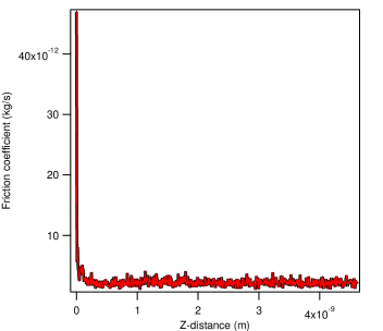
noncontact friction is extremely small, about kg/s,
compared with kg/s of more conventional tuning fork tips
(see Methods for details), which work at smaller distances, just outside the repulsive regime.
Here we use the pendulum to demonstrate a novel example of noncontact friction,
occurring when the vibrating tip pumps integer 2 slips onto the local surface phase of a
CDW.
Layered dichalchogenides have long been known for their phase transitions leading to picometer sized superstructure lattice distortions and corresponding new electronic periodicities in their low temperature ground stateWilson1975 . Among them, NbSe2 (with 2H stacking) stands out as a material exhibiting bulk CDW below the long range order onset temperature K Moncton1975 , as well as superconductivity below K. The CDW consists of a joint periodic lattice distortion (PLD) and electron density modulation, with the same incommensurate periodicity close to in the layer plane, and a remarkably coherent phase, extending over hundreds of lattice spacings in clean samples. Whereas in other isoelectronic compounds of that family, such as TaS2 (with 1T stacking), the CDW has a clear connection with the Fermi surface, thus leading to an insulating or near insulating state at low temperatures Wilson1975 , the driving force in NbSe2 is now known to be different, not directly involving the Fermi surface, as recently ascertained both experimentally Inosov2008 ; Shen2008 ; Borisenko2009 ; Weber2011 ; Pasupathy2013 and theoretically Weber2011 . The distortion of NbSe2 is thus really only a PLD. Nonetheless we stick to the commonly used term “CDW” to avoid language confusion.
We measured the friction force acting between an in situ cleaved NbSe2 surface and a sharp silicon cantilever tip oscillating in the pendulum geometry as well as a qPlus tuning fork tip. We simultaneously acquired the tip oscillation frequency and a dissipation signal under ultrahigh-vacuum (UHV) conditions and low temperatures of K, at which CDW and superconductivity coexist. As a function of tip-surface distance, we observed a remarkable train of dissipation maxima which extend as far out as a few nm above the surface. In order to understand their origin we consider a theoretical model, where the CDW is treated as an elastic medium coupled to the spatially extended oscillating cantilever tip (Fig. 1(a)). A comparison of AFM data with theory allows us to conclude that the series of dissipation maxima is due to a hysteretic behavior of the CDW phase as the tip oscillates at specific distances where sharp local slips occur.
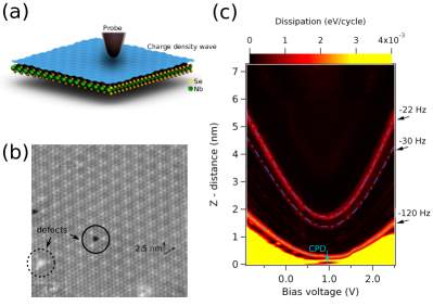
We first obtained, by means of a standard tuning fork STM, the atomically resolved surface topography showing the additional CDW induced Moiré pattern as shown in Fig. 1(b). The CDW modulation is incommensurate with the underlying lattice, as is well known Moncton1975 ; Guillamon2008 . Depending on the chosen spot, the CDW modulation is known to exhibit its incommensurate deviation from the nearby commensurate periodicity either along one, or simultaneously along all three, planar directions Soumyan2013 . In the proximity of the few visible surface defects (CO adsorbates and Se vacancies) the CDW distortion, pinned by the impurity, survives well above the pristine .
In Fig. 1(c) the noncontact friction versus tip-sample distance and tip-sample voltage as the tip approaches the sample surface is shown for the pendulum AFM. The dissipated power in units of electron volts per cycle is calculated according to a standard formula, measuring the difference between the power in (first term) and out (second term) of the tipCleveland1998 :
| (1) |
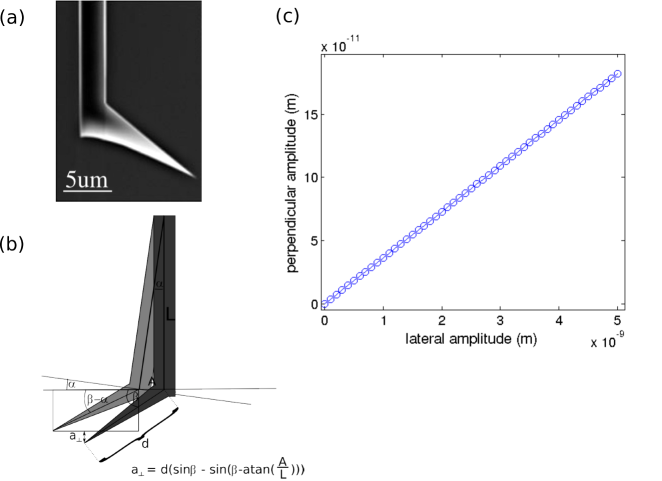
where is the dissipated power due to intrinsic losses of the cantilever, measured at large tip-sample separation, and are the distance dependent excitation amplitude (as measured by the excitation voltage needed to excite the cantilever at constant oscillation amplitude ) and frequency of the cantilever and the suffix zero refers to the free cantilever. In the case of pendulum AFM, the frequency and the amplitude of lateral oscillations are equal to kHz and nm, respectively. Owing to the tip asymmetry (see Methods section and Supplementary material), there is a non negligible perpendicular oscillation amplitude pm as well. Bright features on Fig. 1(c) correspond to high dissipation maxima up to meV/cycle observed already at some nm above the sample surface. Within each dissipation branch the amount of energy loss stays constant, independently of the bias voltage . The giant noncontact friction maxima remain well defined even after careful compensation of Contact Potential Difference (CPD) between tip and sample. The peaks persist whether the tip-surface interaction force is van der Waals ( V) or electrostatic (). Moreover, the voltage dependence of each dissipation branch has a parabolic behavior (as expected for an electrostatic capacitive interaction between a roughly conical tip and sample, where ) implying that each dissipation maximum always occurs at the same tip-surface interaction force as the voltage changes. Thus the effect is force controlled rather than voltage controlled.
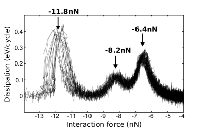
So far the pendulum AFM results. To further confirm and ascertain the universal nature of this new effect, we repeat the experiment on an alternative instrument, the tuning fork AFM. In this setup, the tip oscillation direction is perpendicular to the sample surface, making the measurement more localized and ultimately more consistent across the surface. Fig. 2 shows the non contact friction of this different probe, again as a function of ( V V), and the dissipated power again calculated according to equation (1), where kHz and pm. Tuning fork results systematically show three reproducible dissipation maxima positioned at different interaction forces nN, nN, nN as the tip approaches the surface (distance nm nm and the attractive force was extracted from the cantilever frequency data by means of the Sader-Jarvis algorithm sader2004 ). The finding of sharp dissipation peaks, a single one of which was already reported by Saitoh Saitoh2010 , is contrary to most noncontact friction experiments, where the energy dissipation increases smoothly as the interaction force rises Kisiel2011 ; Volo2007 ; Stipe2001 ; Kuehn2006 . In particular, tip dissipation on a NbS2 sample, yet another layered dichalcogenide compound, but without CDW, shows only a smooth increase (see Supplementary material). In summary two independent UHV experiments - the pendulum AFM (Fig. 1(c)) and – with much smaller intensity– the tuning fork AFM (Fig. 2) - find a sequence of dissipation peaks extending as far out as several nm above the surface.
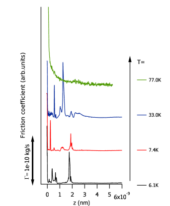
What is their origin? Even before any theory, temperature provides a suggestion that the dissipation peaks are related to the coupling of the tip to the CDW distortion. The dissipation peaks in fact survive up to a temperature of about K (see Fig. 3 of the Supplementary Materials). As mentioned earlier, STM data show that short-range CDW order in NbSe2 persists around surface defects or impurities at temperature up to Pasupathy2013 . Up to that temperature, the tip potential itself may thus awaken a local CDW distortion, which can in turn display similar dissipation phenomena to the long-range ordered CDW.
To model and understand in detail the effect of the tip on the CDW, and ultimately the source of the dissipation peaks, we describe the density deformation as a simple elastic system interacting with an extended perturbation. Following well established literature Fukuyama1978 ; Lee1979 , we describe the CDW through phase and amplitude order parameters, the latter assumed constant for small perturbations. The overall density (ions and electrons) takes the form , where is the wavenumber and the constant amplitude. The energy as a function of the order parameter for an external perturbing tip potential then reads:
| (2) |
To keep it simple, this description assumes a unidirectional CDW, but the same mechanism should hold in our tridirectional NbSe2 experimental example. For a given external potential, the energy can be minimized to find the preferred phase shape along x. The main difference with previous treatments that were given for impurities Tucker1989 is that in this case, due to the large size of the pendulum tip and swing, the potential may extend over lengths longer than the characteristic CDW lengthscale 2.5 nm: this leads to new interesting effects. Additional care needs to be taken in choosing the dimensionality of the system: while the relevant tip-related behavior of the CDW is along x and restricted to the surface, a full treatment will have to take into account the other dimensions, namely y in the surface plane, and z into the underlying bulk, in order to obtain a realistic shape for the order parameter. While these aspects will be discussed in a separate work, here we will describe the effect in a simple one dimensional model, which retains all the necessary features without any of the complications connected with a higher dimensionality.
An important role in understanding the dissipation mechanism is played by the boundary conditions: while we will impose the phase to be fixed at the boundaries (consistently with an overall pinned CDW as known experimentally), this value is only defined modulo . This leads to the existence of qualitatively different solutions of the energy minimization problem, where (along the main CDW direction) the perturbation may lead to a phase change , with integer, between the pinned boundaries. We will call the “winding number” of a given order parameter configuration. We minimize the energy in the subspace of one given winding number and observe its behavior as a function of the perturbation amplitude, controlled by the tip position above the substrate. We show this energy in Fig. 3 for a perturbation of Lorentzian form , mimicking an approaching conical tip, as a function of the tip-sample distance .
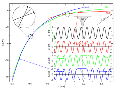
As energy curves for different winding numbers sharply cross at specific distances, marked by dashed circles, we expect the CDW phase winding number to switch from one to the next type of deformation at these points. Moreover, as shown in the inset (phase and density along the main CDW direction for different ), these solutions present a qualitative difference, akin to a symmetry difference, making a smooth transition between the two impossible. Passing through a crossover point will thus be accompanied by a hysteresis cycle in the tip mechanics, which explains the giant size of dissipation peaks despite the extremely low tip oscillation frequency as compared to dielectric relaxation frequency ( MHz) measured in ac-conductivity experiments Tucker1989 . To corroborate this picture, let us consider the height of the dissipation peaks it would produce, proportional to the area of the hysteresis cycle. We expect this area to be related to the angle between the energy curves and the average slope at the crossing point (see the blow up in Fig. 3). Considering that the area of the hysteresis cycle while oscillating around this point will behave like , we see from the shape of the curves that the variation of these two parameters have opposite effects on the height of the peak as the tip approaches the surface, since a decreasing would decrease the hysteresis area, while an increasing would increase it. This provides a possible explanation of the non-monotonic peak intensity behavior observed experimentally. A full treatment of the CDW related dissipation materials should be followed by a more thorough theoretical treatment, which will be reported elsewhere. We can conclude here that the CDW phase slip model reproduces, at least qualitatively, the basic characteristics of the observed dissipation.
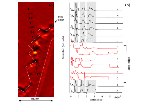
It is important before closing to make connection with earlier work, both experimental Saitoh2010 , where a single dissipation peak was reported on NbSe2 and SrTiO3, and theoretical She2012 , where a collective resonance of spin-like centers was ingeniously invoked to explain it. Our findings of a multiplicity of interaction force-controlled peaks in NbSe2, peaks systematically absent over NbS2, suggests a different scenario. The train of peaks is perfectly reproducible and ubiquitous over well ordered surfaces and clean NbSe2 bulks, making the existence and nature of these centers doubtful (see Fig. 4 of the Supplementary Material). The temperature evolution of the peaks suggests instead a strong connection with the CDW. A correspondence between each peak and the local pumping of a CDW phase slip is made especially compelling by theoretically finding a first order energy crossing of states of the CDW with different winding numbers, implying the possibility of a mechanical hysteresis cycle even at the very low tip vibration frequency, where an alternative viscous dissipation could be barely detectable at best. In summary we believe we identified a promising mechanism – coupling of a slider to a collective phase – that is novel and deserves further experimental and theoretical study, extending to other systems with incommensurate bulk phases. It should apply in particular to genuine charge-density-wave and spin-density-wave materials, where the phase pumping should entail interesting surface flows of charge and spin under vibrating tips.
Methods
Sample
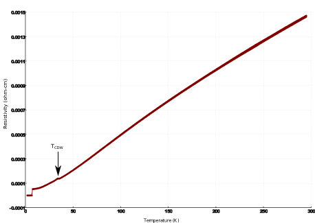
We used a high quality 2H-NbSe2 single-crystal sample of size mm3 with a K determined from temperature dependent resistance measurements which is in agreement with previous results Lin2005 . The crystal was produced by means of standard chemical vapor transport technique with iodine as the transport agent Kershaw1967 . The residuals were washed off the surface with solvents. Sample was cleaved under UHV conditions.
Pendulum AFM microscope
The experimental setup used for measuring friction at low temperature is described in details in another publication gysin2011 . Here we note that the probe consisted of a soft cantilever (ATEC-CONT from Nanosensors) with spring constant mN/m. The probe was suspended perpendicularly to the surface with an accuracy of and operated in the so-called pendulum geometry in which the tip vibrational motion is parallel to the sample surface. The oscillation amplitude nm of the tip was kept constant using a Nanonis phase locked loop (PLL) feedback system. The cantilever tip is asymmetric as shown in Supplementary material. Due to this the perpendicular component of oscillation amplitude pm exists as well. The cantilever was annealed in UHV up to C for hours, which results in the removal of water layers and other contaminants from both cantilever and tip. This is confirmed by the improvement of the quality factor of the probe by almost 2 orders of magnitude nt_rast06 . It is also known that this long-term annealing leads to negligible amounts of localized charges on the probing tip. After annealing the cantilever was characterized by a resonance frequency kHz and a quality factor . This lead to the internal friction kg/s and the corresponding dissipated power W (at K). The sample and cantilever temperatures were controlled by means of two different cryogenic controllers (Model 340 and Model DRC-91C from Lakeshore Cryotronics, Inc., Westerville, Ohio, USA).
Tuning-fork based STM/AFM
The STM/AFM experiments were performed with a commercial qPlus STM/AFM microscope (Omicron Nanotechnology GmbH) running at low temperature ( K) under UHV and operated by a Nanonis Control System from SPECS GmbH. We used a commercial tuning fork sensor in the qPlus configuration (typical parameters: resonance frequency kHz, spring constant N/m, typical quality factor at K). The oscillation amplitude was always set to pm. The oscillation frequency and excitation amplitude were recorded simultaneously for different values applied to the tungsten tip. The force extraction was done by means of the Sader and Jarvis formula sader2004 . Additional curve was taken (typical retraction distance nm) after the complete spectroscopic measurement in order to estimate the long-rage vdW background. All STM images were recorded in the constant current mode.
Theoretical treatment
The energy given in equation (2) was minimized numerically through a simple conjugated gradient algorithm numrec on a two-dimensional discrete grid. The CDW was taken as unidirectional, while the other direction is required for a realistic minimization of the phase. Different boundary conditions were enforced to obtain solutions with different winding number , while within the grid the gradient was considered modulo to allow for phase jumps when . The external potential was taken as a Lorentzian depending on the tip-sample distance as , with and . This shape is found to be appropriate to model a conical tip interacting with the surface through van der Waals force. The parameters are estimated from a fit of the experimental overall tip-sample interaction within the same model.
Acknowledgements
FP, GES, and ET acknowledge research support by MIUR, through PRIN-2010LLKJBX_001, by SNSF, through SINERGIA Project CRSII2 136287/1, and by the EU-Japan Project LEMSUPER. ET acknowledges ERC Advanced Research Grant N. 320796 MODPHYSFRICT. RB acknowledges financial support by the CNR program Short Term Mobility STM 2011. ML, MK, RP, AB, and EM acknowledge financial support from the Swiss National Science Foundation (NSF), the SINERGIA Project CRSII2 136287/1 and the Swiss National Center of Competence in Research on “Nanoscale Science” (NCCR-NANO).GB acknowledges financial support from EPSRC, UK(EP/I007210/1).
Author contributions
The samples was fabricated by GB. The idea was born out of discussion between ET, EM, RB, AG, RP and MK. The experiment was carried out by ML, MK and RP. RB and AG participated in sample preparation and pendulum AFM experiment. The theoretical model was developed by FP, GES and ET. ET, EM, AB, FP, GES, RB, AG, ML, MK and RP were involved in interpretation, discussion and paper writing.
References
- (1) M. Urbakh and E. Meyer, Nanotribology: The renaissance of friction. Nature Mat. 9, 8-10, (2010).
- (2) M.A. Lantz, D. Wiesmann, and B. Gotsmann, Dynamic superlubricity and the elimination of wear on the nanoscale, Nat. Nanotech. 4, 586-591 (2009).
- (3) A. Socoliuc, E. Gnecco, S. Maier, O. Pfeiffer, A. Baratoff, R. Bennewitz, and E. Meyer, Atomic-Scale Control of Friction by Actuation of Nanometer-Sized Contacts, Science 313, 207-210 (2006).
- (4) A. Vanossi, N. Manini, M. Urbakh, S. Zapperi, and E. Tosatti, Modeling friction: from nanoscale to mesoscale, Rev. Mod. Phys. 85, 529 (2013).
- (5) M. Kisiel, E. Gnecco, U. Gysin, L. Marot, S. Rast and E. Meyer, Suppression of electronic friction on Nb films in the superconducting state, Nature Mat. 10, 119-122, (2011).
- (6) A. I., Volokitin, B. N. J. Persson, H. Ueba, Giant enhancement of noncontact friction between closely spaced bodies by dielectric films and two-dimensional systems, Journ. Exp. Theor. Phys., 104, 96-110, (2007).
- (7) B.C. Stipe, H.J. Mamin, T.D. Stowe, T.W. Kenny, and D. Rugar, Noncontact Friction and Force Fluctuations between Closely Spaced Bodies, Phys. Rev. Lett. 87, 096801 (2001).
- (8) S. Kuehn, R.F. Loring, and J.A. Marohn, Dielectric Fluctuations and the Origins of Noncontact Friction, Phys. Rev. Lett. 96, 156103 (2006).
- (9) J.A. Wilson, F.J. Di Salvo, and S. Mahajan, Charge-Density Waves and Superlattices in the Metallic Layered Transition Metal Dichalcogenides, Adv. Phys. 24, 117-201 (1975).
- (10) D. E. Moncton, J. D. Axe, and F. J. DiSalvo, Study of Superlattice Formation in -Nb and -Ta by Neutron Scattering, Phys. Rev. Lett. 34, 734 (1975).
- (11) D S Inosov and V B Zabolotnyy and D V Evtushinsky and A A Kordyuk and B Büchner and R Follath and H Berger and S V Borisenko, Fermi surface nesting in several transition metal dichalcogenides, New Journal of Physics, 10, 125027, (2008).
- (12) Shen, D. W. and Zhang, Y. and Yang, L. X. and Wei, J. and Ou, H. W. and Dong, J. K. and Xie, B. P. and He, C. and Zhao, J. F. and Zhou, B. and Arita, M. and Shimada, K. and Namatame, H. and Taniguchi, M. and Shi, J. and Feng, D. L., Primary Role of the Barely Occupied States in the Charge Density Wave Formation of , Phys. Rev. Lett. 101, 226406, (2008).
- (13) Borisenko, S. V. and Kordyuk, A. A. and Zabolotnyy, V. B. and Inosov, D. S. and Evtushinsky, D. and Büchner, B. and Yaresko, A. N. and Varykhalov, A. and Follath, R. and Eberhardt, W. and Patthey, L. and Berger, H., Two Energy Gaps and Fermi-Surface “Arcs” in , Phys. Rev. Lett. 102, 166402, (2009).
- (14) Weber, F. and Rosenkranz, S. and Castellan, J. P. and Osborn, R. and Hott, R. and Heid, R. and Bohnen, K. P. and Egami, T. and Said, A. H. and Reznik, D., Extended Phonon Collapse and the Origin of the Charge-Density Wave in , Phys. Rev. Lett. 107, 107403, (2011).
- (15) S.P. Chockalingam, C.J. Arguello, E.P. Rosenthal, L. Zhao, C. Gutiérrez, J.H. Kang, W.C. Chung, R.M. Fernandes, S. Jia, A.J. Millis, R.J. Cava, A.N. Pasupathy, Visualizing the Charge Density Wave Transition in 2H-NbSe2 in Real Space, arXiv:1307.2282 [cond-mat.str-el], (2013).
- (16) Guillamón, I. and Suderow, H. and Vieira, S. and Cario, L. and Diener, P. and Rodière, P., Superconducting Density of States and Vortex Cores of 2H-, Phys. Rev. Lett. 101, 166407, (2008).
- (17) A. Soumyanarayanan, M.M. Yee, Y. He, J. van Wezel, D.J. Rahn, K. Rossnagel, E.W. Hudson, M.R. Norman, and J.E. Hoffman, Quantum phase transition from triangular to stripe charge order in NbSe2, PNAS 110, 1623, (2013).
- (18) J. P. Cleveland, B. Anczykowski, A. E. Schmid, and V. B. Elings, Energy dissipation in tapping-mode atomic force microscopy Appl. Phys. Lett. 72, 2613 (1998).
- (19) John E. Sader and Suzanne P. Jarvis, Accurate formulas for interaction force and energy in frequency modulation force spectroscopy, Applied Physics Letters 84, 1801-1803, (2004).
- (20) K. Saitoh, K. Hayashi, Y. Shibayama, K. Shirahama, Gigantic Maximum of Nanoscale Noncontact Friction, Phys. Rev. Lett.105, 236103, (2010).
- (21) Fukuyama, H. and Lee, P. A., Dynamics of the charge-density wave. I. Impurity pinning in a single chain, Phys. Rev. B 17, 535-541, (1978).
- (22) Lee, P. A. and Rice, T. M., Electric field depinning of charge density waves, Phys. Rev. B 19, 3970-3980, (1979).
- (23) Tucker, J. R. Impurity pinning of sliding charge-density waves, Phys. Rev. B40, 5447-5459, (1989).
- (24) She, Jian-Huang and Balatsky, Alexander V., Noncontact Friction and Relaxational Dynamics of Surface Defects, Phys. Rev. Lett.108, 136101, (2012).
- (25) Lin-jun Li and Zhu-an Xu and Jing-qin Shen and Li-min Qiu and Zhi-hua Gan, The effect of a charge-density wave transition on the transport properties of 2H-NbSe2, Journal of Physics: Condensed Matter 17, 493, (2005).
- (26) Kershaw, R. and Vlasse, Marcus and Wold, Aaron, The preparation of and electrical properties of niobium selenide and tungsten selenide, Inorganic Chemistry 6, 1599-1602, (1967).
- (27) U. Gysin and S. Rast and M. Kisiel and C. Werle and E. Meyer, Low temperature ultrahigh vacuum noncontact atomic force microscope in the pendulum geometry, Review of Scientific Instruments 82, 023705, (2011).
- (28) S. Rast, U. Gysin, P.Ruff, C. Gerber, E. Meyer and D.W. Lee, Force microscopy experiments with ultrasensitive cantilevers, Nanotech. 17, 189-194 (2006).
- (29) W.H. Press, S.A. Teukolsky, W.T. Vetterling, and B.P. Flannery, Numerical Recipes: The Art of Scientific Computing (3rd ed.), Cambridge University Press (2007).
Supplementary material to CDW slips and giant frictional dissipation peaks at the NbSe2 surface
Additional 5 figures with captions:
- An asymmetric pendulum AFM tip.
- Dependence of resistivity as a function of temperature for NbSe2 sample
used in the experiment.
- Temperature dependence of non-contact friction coefficient on NbSe2
sample.
- Tip-sample position dependence of non-contact friction coefficient as the tip crosses the step edge
of NbSe2 surface.
- Non-contact friction on NbS2 - an intercalated transition metal compound
with no CDW signature.
