Effect of plate roughness on the field near RPC plates
Abstract
The inner surfaces of the electrodes encompassing the gas volume of a Resistive Plate Chamber (RPC) have been found to exhibit asperities with, grossly, three kinds of features. The desired uniform electric field within the gas volume of RPC is expected to be affected due to the presence of these asperities, which will eventually affect the final response from the detector. In this work, an attempt has been made to model the highly complex roughness of the electrode surfaces and compute its effect on the electrostatic field within RPC gas chamber. The calculations have been performed numerically using Finite Element Method (FEM) and Boundary Element Method (BEM) and the two methods have been compared in this context.
1 Introduction
Presence of asperities on the inner surfaces of the gas chamber of a Resistive Plate Chamber (RPC)
is likely to distort the electric field locally which may give rise to spark, dark current etc. and thus
lead to gradual degradation of the detector. Glass or Bakelite® is commonly
used as the resistive plates in a RPC and it has been found to develop some asperities on its surface
in the process of production and handling. The long term operation of the RPCs may also lead to an
increase in the roughness by affecting the surface through various chemical processes. Early R&D
works [1] on Bakelite® RPCs for India-based
Neutrino Observatory (INO) [2] has shown increase in counting rate and decrease in efficiency
with time for the RPCs made of Bakelite® plates without any surface
treatment. Performance of the RPCs improved significantly after treating the inner surfaces with
a suitable fluid.
As the response from an RPC depends critically on the field configuration for a given gas mixture
and environmental conditions, an extensive study on the effect of roughness on the field
configuration is deemed necessary. Such a study will help in deciding the acceptable value of
roughness as well as prediction and interpretation of the experimental data.
In the present work, numerical simulation has been used to estimate this in case of a Bakelite®-RPC. The RPC has been modelled following the design parameters of a prototype
fabricated for INO R&D work. The asperities on the inner surface of the Bakelite® electrode have
been modelled on the basis of the measurement of surface profile of the same Bakelite® grades
used for building the prototype. The calculations have been performed following two numerical methods,
namely, Finite Element Method (FEM) and Boundary Element Method (BEM).
2 Surface Roughness Analysis
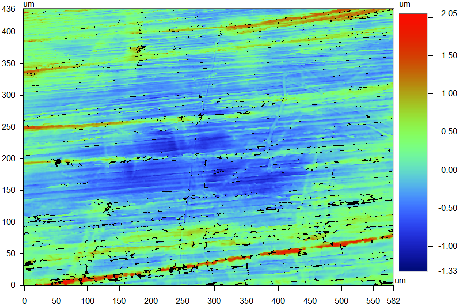
BRUKER ContourGT-K 3D optical microscope has been used to image different samples of a Bakelite® plate. Several samples have been made at several locations with scanning area of dimension 640 m 480 m (shown in figure 1, for example). The surface images are further analyzed using MATLAB [3]. The dimensions of different surface structures have been found out from the color scheme and then 3D images have been generated keeping only those structures whose height crosses a certain color threshold value so that the building blocks of the surface can be seen clearly. The 3D image of figure 1 after MATLAB analysis has been shown in figure 1.
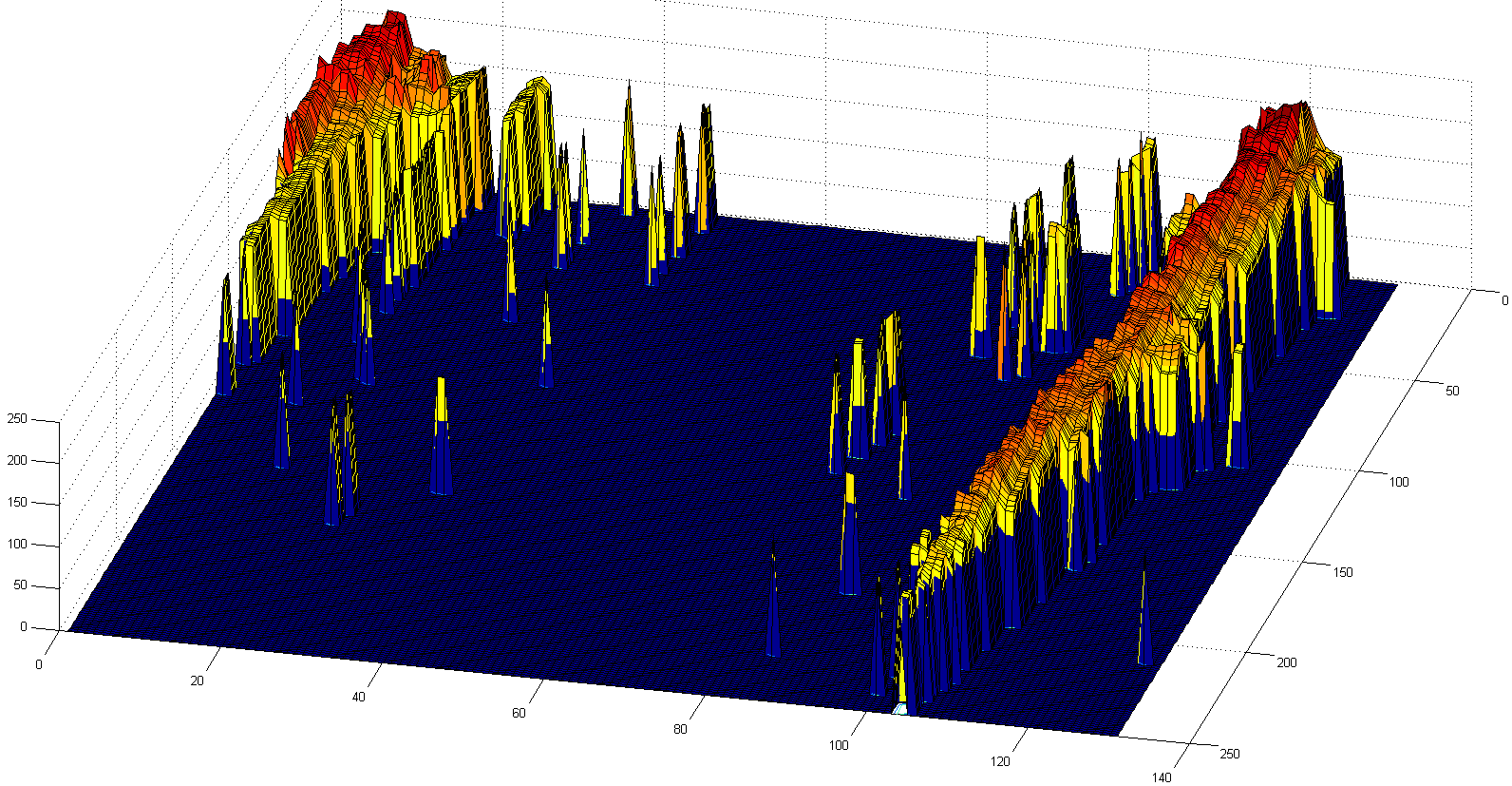
The 3D images of few more measurements have been shown in figure 2 from which the main building blocks of the surface can be found out.
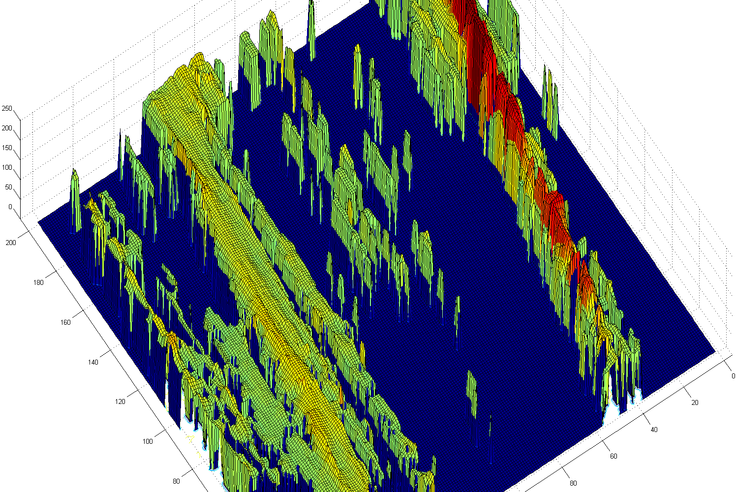
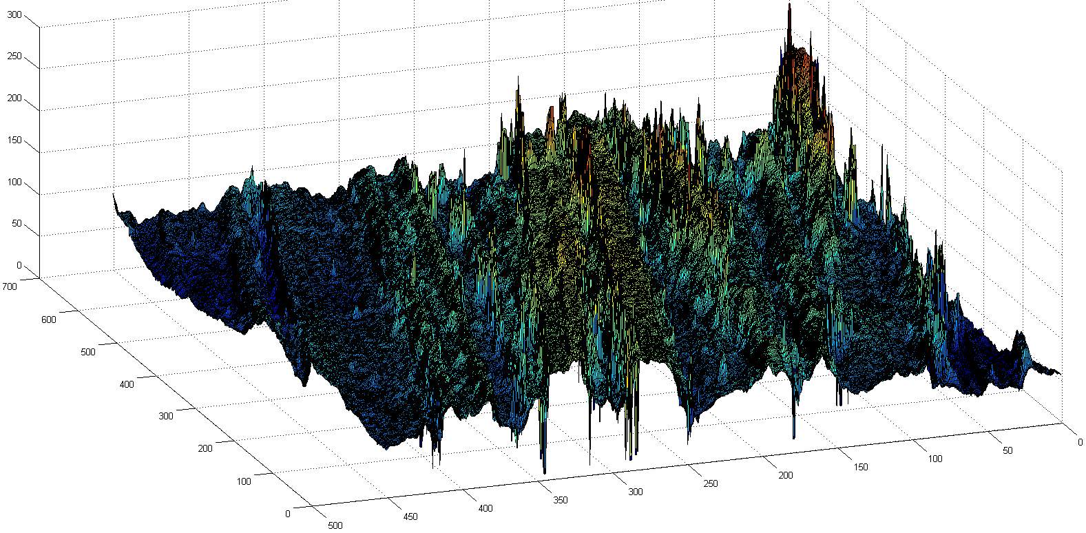
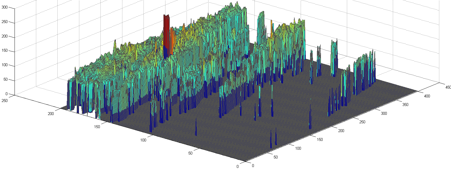
From visual inspection, the following three kind of gross structures in varying dimensions have been found : (i) spike, (ii) ridge and (iii) wave. It has been found out from the data that the average roughness of the surface varies between 150 - 300 nm while the range (distance between the peak and the valley) lies between 1 - 5 m.
3 Numerical Modelling of the Surface
A simplified model of RPC with dimension 5 cm 5 cm, consisting of only the Bakelite® plates and the conductive coats have been modelled to use the computational resources economically, with the mentioned asperities distributed on the inner surface of the upper Bakelite® plate following a definite pattern. A voltage difference of 12 kV has been applied between the coats. The three features of the rough surface along with their modelling scheme have been discussed below:
-
1.
Spike - The randomly distributed spikes have been modelled using boxes of different heights and widths although with a periodic distribution as shown in figure 3. The height and the width of the boxes have been increased individually (along X and Y direction respectively) to a maximum limit of 1 m and 4 m, respectively, and then reduced again to reach the smallest values along the respective directions. For the series of boxes, placed along the diagonal direction both the height and width have been increased in multiples of the smallest box and reduced back to the smallest values. The reason behind the scheme has been to study the individual as well as the combined effect of the variation in height and width of the box in a systematic way.
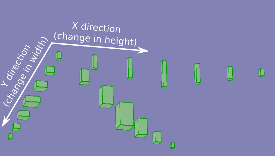
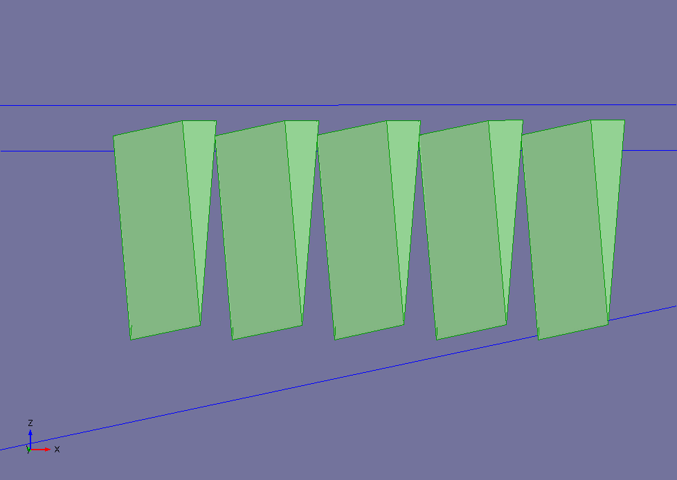
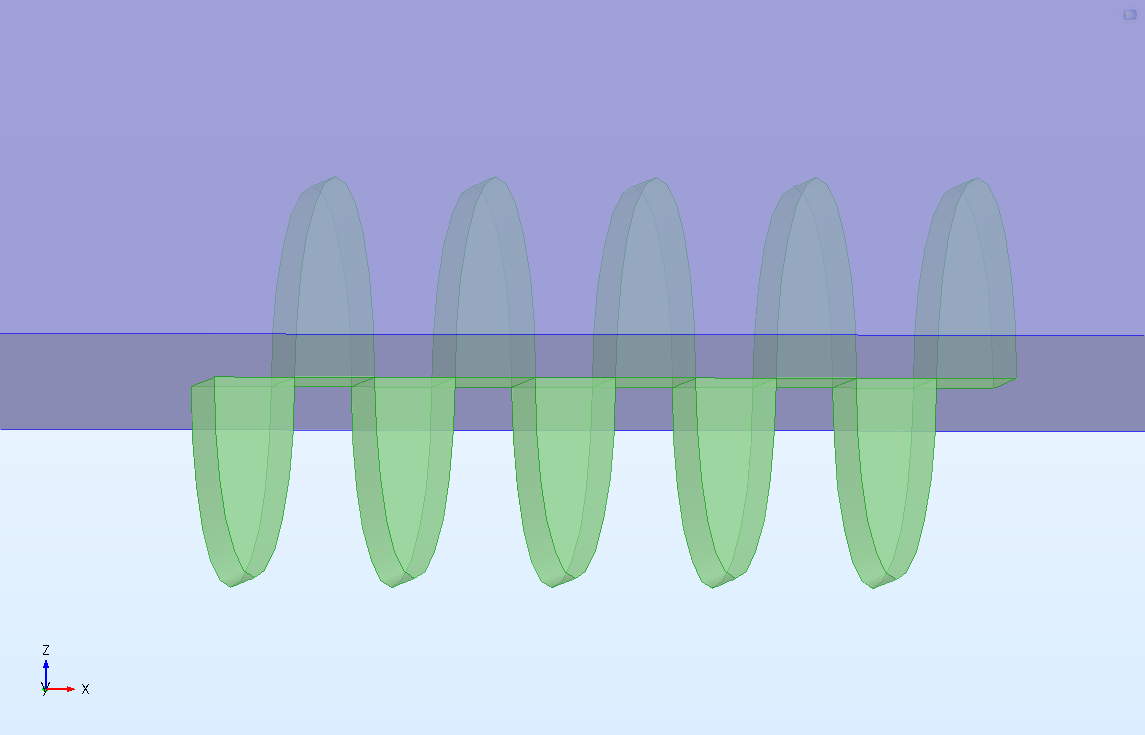
Figure 3: Surface roughness of 3 spike-like structure modelled using a distribution of boxes of different heights and widths (dimension of smallest box: 1 m 1 m 250 nm) separated by 8 m from each other, 3 ridge-like structures modelled using a series of triangular prism-like blocks each of height 5 m, base cross-section 25 m 650 m and a pitch of 50 m, 3 wave-like structure modelled using a sinusoidal wave having amplitude of 10 m and a wavelength of 40 m. -
2.
Ridge - The ridge-like structures have been modelled using five triangular prism-like blocks placed on the inner surface of the upper plate with their sharp edges facing the gas volume as shown in figure 3. The ridges have been placed parallel to each other along the X-direction.
-
3.
Wave - The wave-like feature of the surface has been modelled in the shape of a sinusoidal wave as shown in figure 3. The roughness feature has been incorporated on the upper Bakelite® plate as mentioned earlier with the trenches of depth 10 m implanted on the plate material.
Two different toolkits, COMSOL Multiphysics® [4] v5.2 based
on FEM and neBEM [5] v1.8.16 based on BEM have been used to calculate the field.
In COMSOL®, the whole geometry has been meshed using free tetrahedral
elements except the conductive coating region which has required a special treatment due to its
very small thickness [6].
In neBEM, the surfaces of the geometry have been discretized using rectangular or triangular elements
according to the shape of the geometrical components. The geometry has been built in
Garfield [7] using Constructive Solid Geometry (CSG) approach.
The boxes have been placed 8 m away from each other as an optimum value of separation,
as closer placement requires a finer mesh to resolve the geometry which in turn increases the
consumption of computational resources. Another difficulty in solving the models arises due to the
presence of sharp edges, whose effect can be observed only by using infinitesimally small mesh.
4 Result
All the plots have shown the variation in the value of Z-component of the electric field () for different features of the surface roughness as this is the major component of electric field which can affect the RPC response.
4.1 Effect of the artefacts
The effect of the width and height of the box structures on the nearby electrostatic field, as found from neBEM can be seen from the figures 4 and 4 respectively.
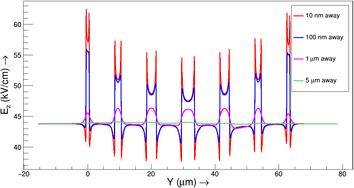
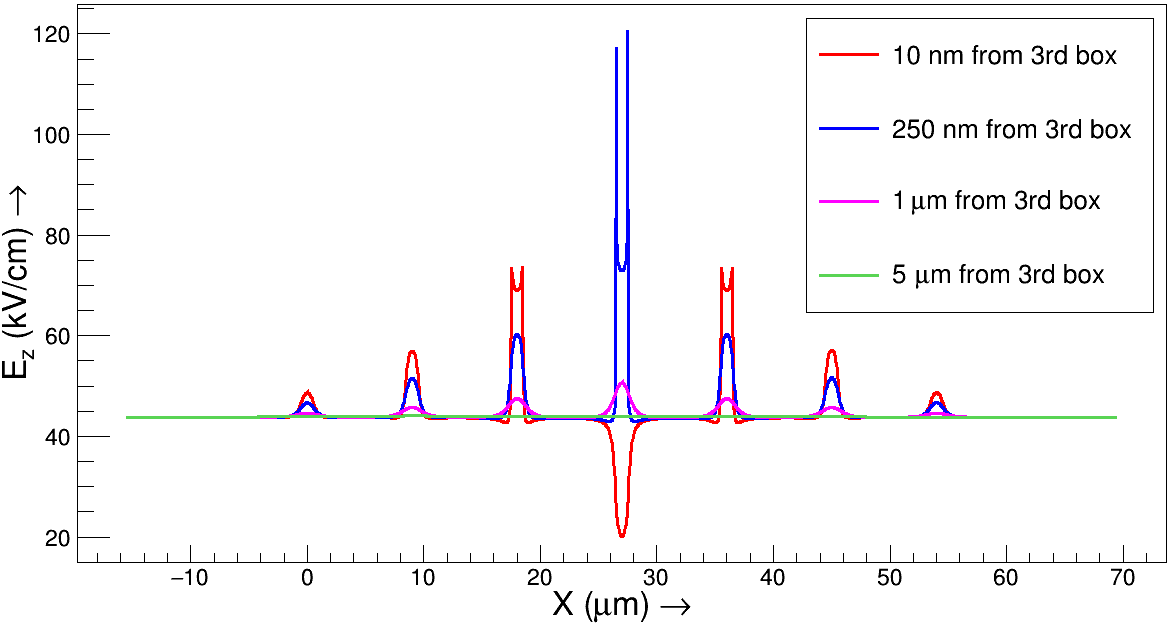
The field is found to increase by 30.5% maximum at 10 nm away and can rise up to 42.8% at the edges while it falls close to the regular value (within 0.6%) around 5 m.
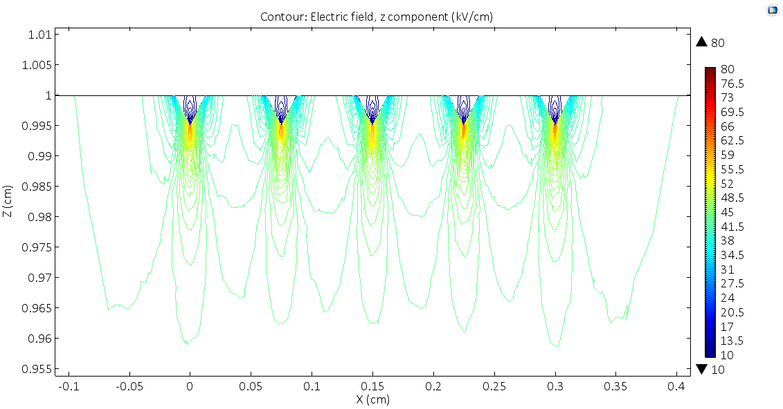
The contour plot of Ez in the vicinity of the ridge-like structures can be seen from the figure
5 as calculated using COMSOL®.
The value of Ez has been found to deviate from the value in a regular region by 46.2% to
0.6% for a distance 10 nm to 50 m away from the structures.
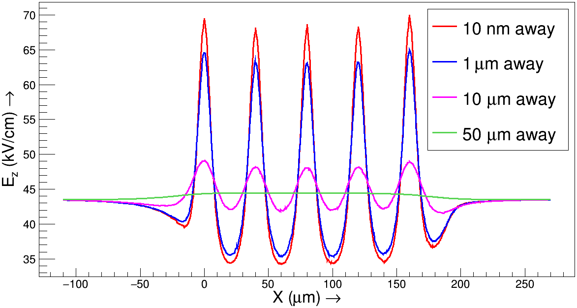
From figure 5, the effect of wavy structure is found up to 50 m
away from the peaks where the relative deviation in the field with respect to its normal
or regular value reduces to 1.9% only while it is 59.2% within 10 nm of the peak and - 21.2% at
the troughs.
4.2 Comparison of FEM and BEM
To compare the two solvers, the value of Ez has been computed for the spike-like structure (see figure 3) using both the solvers and their performance in terms of different parameters has been shown in table 1. In case of COMSOL®, the quoted values are the ones that have been taken by the solver while using the optimized meshing scheme, which itself may be a time-consuming affair. The fifth column of the table shows the convergence criterion for COMSOL® which is the relative error (R.E.) in the calculated values with respect to the set limit (10-5 here) for the last two iterations. COMSOL® has required to iterate 190 times to achieve this. For neBEM, the error has been estimated by finding out the deviation in the calculated values at the collocation points with respect to the given values as obtained from the boundary conditions. The maximum error has been found to be 10-4 on one of the elements in this case.
| Solver | Elements | Time | Memory | Error/ Convergence |
|---|---|---|---|---|
| COMSOL® | 2 106 | 15 mins | 4 GB | 10-5 in 190 iterations |
| neBEM | 17 103 | 2 hours | 8.8 GB | R.E.|max = 10-4 |
5 Summary
The taller and narrower spikes affect the field most, though the affected region stretches with the increase in width. Depending on the shape and size of the asperities the value of electrostatic field near the asperities increases by up to 60% of the regular value. The distortion in the field is found to be confined within a small region (10 - 200 m). This distorted field map is likely to affect the gas transport properties and production of avalanche close to the resistive plates and alter the detector behavior. Considering the overall distribution of asperities on the surface, the detector response near the plates may be significantly altered. As a result the effects of surface asperities need to be studied in further detail and, depending on the results of the study, surface treatment may be planned.
Acknowledgments
We would like to thank Raveendrababu Karanam (IITM) and Dr. Prafulla Behera (IITM) for their help in surface roughness measurements and Prof. Sandip Sarkar (SINP) for his help with the MATLAB analysis. We would also like to thank the members of INO collaboration for their helpful suggestions at different stages of the work and also for the financial support.
References
- [1] S. Biswas et al., Performances of linseed oil-free bakelite RPC prototypes with cosmic ray muons, NIM A 602 (2009) 749.
- [2] ICAL collaboration, Physics Potential of the ICAL detector at the India-based Neutrino Observatory (INO), arXiv:1505.07380, 27/05/2015.
- [3] MATLAB : The Language of Technical Computing, http://in.mathworks.com/products/matlab/.
- [4] COMSOL: a multiphysics simulation tool, www.comsol.co.in.
- [5] N. Majumdar and S. Mukhopadhyay, Simulation of 3D electrostatic configuration in gaseous detectors, 2007 JINST 2 P09006.
- [6] A. Jash et al., Numerical studies on electrostatic field configuration of Resistive Plate Chambers for the INO-ICAL experiment, 2015 JINST 10 P11009.
- [7] Garfield : Rob Veenhof, http://garfield.web.cern.ch/garfield.