Resistance oscillations of two-dimensional electrons in crossed electric and tilted magnetic fields.
Abstract
Effect of electric field on transport of highly mobile 2D electrons is studied in wide GaAs single quantum wells placed in titled magnetic fields. The study shows that in perpendicular magnetic field resistance oscillates due to electric field induced Landau-Zener transitions between quantum levels that corresponds to geometric resonances between cyclotron orbits and periodic modulation of electron density of states. Magnetic field tilt inverts these oscillations. Surprisingly the strongest inverted oscillations are observed at a tilt corresponding to nearly absent modulation of the electron density of states in regime of magnetic breakdown of semiclassical electron orbits. This phenomenon establishes an example of quantum resistance oscillations due to Landau quantization, which occur in electron systems with a density of states.
The quantization of electron motion in magnetic fields generates a great variety of fascinating transport phenomena observed in condensed materials. Shubnikov-de Haas (SdH) resistance oscillations1 and Quantum Hall Effect (QHE)2 are famous examples related to the linear response of electrons. Finite electric fields produce remarkable nonlinear effects. At small electric fields Joule heating strongly modifies the 2D electron transport 3; 4; 5; 6 yielding exotic electronic states in which voltage (current) does not depend on current 7; 8; 9 (voltage10). Application of a stronger electric field produces spectacular resistance oscillations.11; 12; 13; 14; 15; 16 The oscillations are periodic with the electric field and obey the following relation:
| (1) |
where is electron charge, is the radius of cyclotron orbits of electrons at Fermi energy , is a positive integer and factor . These oscillations are related to impurity assisted Landau-Zener transitions between Landau levels titled by the electric field11 and can be treated as geometrical resonances between cyclotron orbits and spatially modulated density of states.17; 18
2D electron systems with multiple populated subbands exhibit additional quantum magnetoresistance oscillations.19; 20; 21; 22; 23; 24; 25; 26 These magnetointersubband oscillations (MISO) are due to an alignment between Landau levels from different subbands and with corresponding bottom energies and . The level alignment produces resistance maximums at the condition
| (2) |
where and the index is a positive integer27; 28; 29; 30. At a half integer Eq.(2) corresponds to resistance minimums occurring at nearly constant density of states (DOS) for broad levels.29; 30
An application of in-plane magnetic field to the muti-subband systems creates significant modifications of electron spectra leading to fascinating beating pattern of SdH oscillations and magnetic breakdown of semiclassical orbits31; 32; 33; 34; 35; 36; 37. Recently it was shown that MISO are strongly modified by the in-plane magnetic field leading to a spectacular collapse of the beating nodes due to magnetic breakdown40.
In this paper we present investigations of the effect of the electric field on electron transport in three-subband electron systems placed in tilted magnetic fields. The study reveals that the in-plane magnetic field inverts the electric field induced resistance oscillations described by Eq.(1). The strongest inverted oscillations are observed at the HF-MISO nodes in the regime of magnetic breakdown, in the of the modulations of the density of states at the fundamental frequency . At these conditions the dissipative resistance reaches a minimum value, which is smaller than the resistance at zero magnetic field.
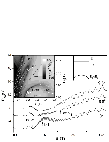
Selectively doped GaAs single quantum well of width 56 nm was grown by molecular beam epitaxy on a semi-insulating (001) GaAs substrate. The heterostructure has three populated subbands with energies at the bottoms of the subbands. The energy diagram are schematically shown in the insert to Figure 1. Hall bars with width m (-direction) and distance m (-direction) between potential contacts demonstrating electron mobility 1.6 106 cm2/Vs and total density =8.8 1015 m-2 were studied at temperature 4.2 Kelvin. The magnetic field, , was directed at different angles relative to normal to the samples and perpendicular to the electric current. Hall resistance yields the angle , where is the perpendicular magnetic field. Current =1A at 133 Hz was applied through the current contacts and the longitudinal and Hall voltages ( and ) were measured in response to a variable dc bias applied through the same current leads. The measurements were done in the linear regime in which the voltages are proportional to yielding differential resistance . Samples A and B with slightly different gaps: =0.43 meV and =0.50 meV were studied.
Figure 1 presents a dependence of the resistance on the perpendicular magnetic field at different angles as labeled. At =0o the resistance shows low frequency (LF-MISO) and high frequency (HF-MISO) MISO.38; 39 LF-MISO correspond to the scattering between the two lowest symmetric (1) and antisymmetric (2 ) subbands and obey the relation .40 HF-MISO corresponds to scattering between either lowest and the third subband. Due to the mismatch between gaps: , HF-MISO show a beating pattern correlated with LF-MISO. In particular the nodes of HF-MISO beating are located at LF-MISO minimums. A parallel magnetic field, , moves nodes at =1/2 and =3/2 toward each other leading to collapse at =9.5o. Insert to Fig.1 shows that odd LF-MISO maximums are bounded by the nodal lines.40
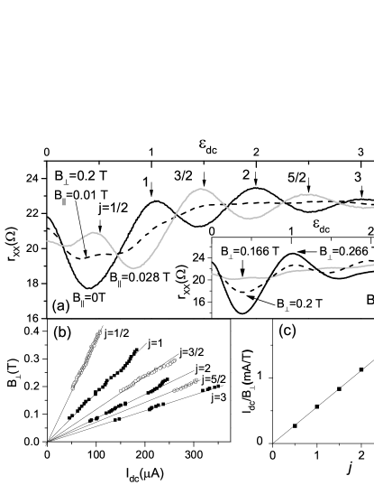
Figure 2 presents dependencies of the differential resistance on the electric field at =0.2 T and different in-plane magnetic fields as labeled taken along the white arrow shown in the left insert to Fig.1.41 At =0 T the black solid line shows three maximums at =1,2 and 3, which obey Eq.(1). The gray solid line presents the dependence taken at the end of the white arrow in the vicinity of the nodal line. This dependence is inverted with respect to the black line and demonstrates maximums at =1/2, 3/2 and 5/2. These maximums also obey Eq.(1) with the fundamental periodicity 1/ but at the half integer values of the index . The dashed line presents the dependence at an intermediate field, which does not display considerable oscillations.
The insert to Fig.2 demonstrates the evolution of the electric field induced resistance oscillations taken along the black arrow shown in Fig.1. This evolution is due to variations of the perpendicular magnetic field, , at =0 T. These curves do not display an inversion. In contrast to the previous case at =3/2 node the resistance oscillations cease at the fundamental frequency () and only weak oscillations at second harmonics () are visible. This behavior is expected. Indeed in accordance with Eq.(2) =3/2 LF-MISO minimum and HF-MISO node correspond to the condition . At this condition symmetric and antisymmetric subband Landau levels are shifted by 3/2 with respect to each other and, therefore, are equally spaced by near the Fermi energy. 40 At =3/2 the fundamental harmonic of the density of electron states (DOS) at frequency is absent. Due to a small Dingle factor the amplitude of the second harmonic of DOS is exponentially small producing very weak geometric resonances with cyclotron orbits at frequency .42 The described behavior of the DOS is valid along all nodal lines40 so the observed inversion of resistance oscillations is intriguing.
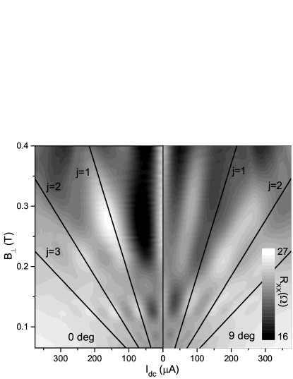
The absence of the inversion at =0T suggests that the effect may have a relation to the magnetic breakdown of quasiclassical orbits.32; 33; 40; 43; 44; 45; 46; 47; 48 Figure 3 supports this proposal. The figure presents an overall behavior of the electric field induced resistance oscillations vs applied dc bias and taken at two different angles. At =0o magnetic breakdown is absent32; 40 and the oscillations obey Eq.(1) with integer indexes . Solid black lines present the theoretical dependence.11; 17; 18 The magnitude of the dc bias induce resistance oscillations is modulated by MISO. At LF-MISO minimum =3/2 (=0.166 T) the oscillations are almost absent (see also insert to Fig.2) and are strongest in the vicinity LF-MISO maximums at =1 and 2. While at angle =9.5o similar oscillations are seen in small , the striking inversion of the oscillations is obvious at 0.166 T. Estimations indicate a 33% probability of magnetic breakdown at =0.3 T and less than 3% at =0.166 T.32; 40
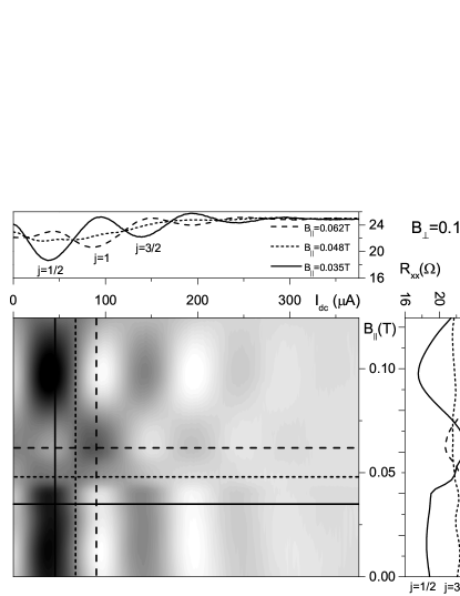
Figure 4 presents the evolution of the dc bias induced resistance oscillations for sample B taken in a vicinity of =2 LF-MISO maximum at =0.166 T and different . The obtained data demonstrate a re-inversion of the resistance oscillations suggesting a periodicity of the inversion with the in-plane magnetic field. Surprisingly oscillations of SdH amplitude in in-plane magnetic fields with a similar period have been recently observed (see Fig.8 in40). These amplitude oscillations are related to periodic oscillations of the subband splitting in strong magnetic fields.32; 49; 50; 51; 52 The right panel indicates that at 3/4 almost no resistance oscillations are induced by . The upper panel shows that this absence of oscillations holds at , where is a positive integer.
A theory of the observed inversion of dc bias induced resistance oscillations is not available. Below a qualitative model is proposed. Studied wide GaAs quantum wells are considered as two 2D parallel systems separated by a distance in -direction and the coupling between the systems is treated in tight binding approximation using a tunneling magnitude .32; 40 At =0 T electrons occupy symmetric (S) and antisymmetric(AS) subbands and move in plane along cyclotron orbits with radius at the Fermi energy. In the lateral electron motion is quantized and the eigenfunctions can be presented as , where =S,AS and =0,1,2… numerates Landau levels.40 An application of the in-plane magnetic field mixes the symmetric and antisymmetric states. In the vicinity of the nodal line surrounding =1 region eigenfunctions are well approximated by a linear combination of one symmetric and one antisymmetric states (see Fig.10 in40), which for simplicity of the presentation we consider to be equally populated: =(+)/, where index numerates ascending energy levels. Figure 5(a) presents an evolution of the electron spectrum along the black and white arrows shown in Fig.1. The evolution corresponds to numerical computations of the spectrum in the vicinity of Fermi energy40.
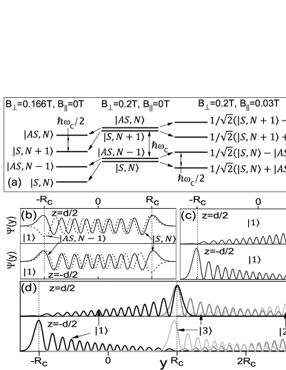
Resistance oscillations are observed at high filling factors and, thus, the semiclassical treatment is appropriate. It is accepted that the main contribution to dc bias induced resistance oscillations comes from electron backscattering by impurities.11; 17; 18 The backscattering occurs near the turning points of the cyclotron orbits displaced by distance 2 along the electric field . The electron spends a considerable amount of time at these points and the overlap between incident and scattered electron orbits is maximized.17; 18; 53; 54 Below we analyze the spatial structure of eigenfunctions.
Figure 5(b) shows the wave function =(+-)/ for top (=) and bottom (=) 2D layers at =16. Since is even the wave function (-) is symmetric (antisymmetric) in both and -directions. The eigenfunction is a sum of these two functions that leads to the spatial electron distribution shown in Fig.5(c): at the left (right) turning point of the oscillator state an electron is located mostly in the bottom (top) 2D layer at (). A similar configuration is obtained for state while the electron distribution in state is the distribution in state rotated by 180o around the =0 axes.
The electric field tilts the spectrum in -direction (not shown) that allows horizontal transitions between the levels due to elastic impurity scattering, which is considered as a local perturbation.11; 17; 18 The impurity backscattering near the turning points changes the direction of electron velocity by , which is accomplished by an overlap between the incoming state near a turning point and the outgoing state located near the turning point of the oscillator shifted by 2 . Illustrating this statement Fig.5(d) indicates that the wave functions of the states and overlap at the opposite turning points, which leads to backscattering while the backscattering between states and is significantly suppressed since these wave functions at the opposite turning points are located in 2D layers and, thus, the overlap between two functions is exponentially small. Similar consideration indicates the presence (absence) of backscattering between states and with different (the same) parity of indexes: (). At nodal lines the energy difference between states with different index parity obeys the relation: , that leads to the relation: for the electric field induced resistance oscillations in tilted magnetic field.
At zero dc bias the backscattering occurs inside the same quantum level. Thus in tilted magnetic fields the impurity backscattering in the linear response is suppressed at the nodal lines since the parity of the incoming and outgoing states is the same. This conclusion is in agreement with the experiment. Indeed Fig.1 shows that at the HF-MISO node located at =0.2T and =0.033 T the resistance reaches a value which is than the value of the resistance both at =3/2 at =0 T and even at zero magnetic field. The data indicates that electron backscattering by impurities is effectively by in-plane magnetic field. This result may have important implications for the field of topological insulators, where electron backscattering is considered to be crucial.
In conclusion the electric field induced resistance oscillations are studied in wide GaAs quantum wells placed in tilted quantizing magnetic field. The oscillations are related to impurity assisted Landau-Zener transitions between quantum levels and in perpendicular magnetic fields obey relation: , where is a positive integer. A tilt of the magnetic field inverts the oscillations. The strongest inversion occurs at the nodal line of the beating between magnetointersubband resistance oscillations at which the density of electron states is nearly constant. These oscillations obey the relation , where is a positive half integer. The effect is related to spatial redistribution of eigenfunctions of multi-subband electron systems leading to modification of the electron backscattering in tilted magnetic fields.
This work was supported by the National Science Foundation (Division of Material Research - 1104503), the Russian Foundation for Basic Research (project no.14-02-01158) and the Ministry of Education and Science of the Russian Federation.
References
- (1) D. Shoenberg Magnetic oscillations in metals, (Cambridge University Press, 1984).
- (2) Sankar D. Sarma, Aron Pinczuk Perspectives in Quantum Hall Effects, (Wiley-VCH, Weinheim, 2004).
- (3) Jing-qiao Zhang, Sergey Vitkalov, A. A. Bykov, A. K. Kalagin, and A. K. Bakarov Phys. Rev. B 75, 081305(R) (2007).
- (4) Jing Qiao Zhang, Sergey Vitkalov, and A. A. Bykov Phys. Rev. B 80, 045310 (2009).
- (5) N. C. Mamani, G. M. Gusev, O. E. Raichev, T. E. Lamas, and A. K. Bakarov, Phys. Rev. B 80, 075308 (2009).
- (6) I. A. Dmitriev, M.G. Vavilov, I. L. Aleiner, A. D. Mirlin, and D. G. Polyakov, Phys. Rev. B 71, 115316 (2005).
- (7) A. A. Bykov, Jing-qiao Zhang, Sergey Vitkalov, A. K. Kalagin, and A. K. Bakarov Phys. Rev. Lett. 99, 116801 (2007).
- (8) W. Zhang, M. A. Zudov, L.N. Pfeiffer, and K.W. West, Phys. Rev. Lett. 100, 036805 (2008).
- (9) G. M. Gusev, S. Wiedmann, O. E. Raichev, A. K. Bakarov, and J. C. Portal Phys. Rev. B 83, 041306 (2011).
- (10) A. A. Bykov, Sean Byrnes, Scott Dietrich, Sergey Vitkalov, I. V. Marchishin and D. V. Dmitriev, Phys. Rev. B 87, 081409(R) (2013).
- (11) C. L. Yang, J. Zhang, R. R. Du, J. A. Simmons, and J. L. Reno, Phys. Rev. Lett. 89, 076801 (2002).
- (12) A. A. Bykov, J. Q. Zhang, S. Vitkalov, A. K. Kalagin, and A. K.Bakarov, Phys. Rev. B 72, 245307 (2005).
- (13) W. Zhang, H. S. Chiang, M. A. Zudov, L. N. Pfeiffer, and K. W. West, Phys. Rev. B 75, 041304 (2007).
- (14) A. T. Hatke, M. A. Zudov, L. N. Pfeiffer, and K. W. West, Phys. Rev. B 83, 081301(R) (2011).
- (15) A. V. Goran, A. K. Kalagin, and A. A. Bykov, JETP Lett. 94, 535 (2011).
- (16) Scott Dietrich, Sean Byrnes, Sergey Vitkalov, A. V. Goran, and A. A. Bykov Phys. Rev. B 86, 075471 (2012).
- (17) M. G. Vavilov, I. L. Aleiner, and L. I. Glazman, Phys. Rev. B 76, 115331 (2007).
- (18) M. Khodas and M. G. Vavilov, Phys.Rev.B 78, 245319 (2008).
- (19) P. T. Coleridge, Semicond. Sci. Technol. 5, 961 (1990).
- (20) D. R. Leadley, R. Fletcher, R. J. Nicholas, F. Tao, C. T. Foxon, and J. J. Harris, Phys. Rev. B 46, 12439 (1992).
- (21) A. A. Bykov, D. R. Islamov, A. V. Goran, A. I. Toropov, JETP Lett. 87, 477 (2008).
- (22) A. A. Bykov, JETP Lett. 88, 64 (2008).
- (23) A. A. Bykov, JETP Lett. 88, 394 (2008).
- (24) N. C. Mamani, G. M. Gusev, T. E. Lamas, A. K. Bakarov, O. E. Raichev, Phys. Rev. B 77, 205327 (2008).
- (25) A. A. Bykov, JETP Lett. 89, 461 (2009).
- (26) A. V. Goran, A. A. Bykov, A.I. Toropov, S. A. Vitkalov, Phys. Rev. B 80, 193305 (2009).
- (27) L. I. Magarill and A. A. Romanov, Sov. Phys. Solid State 13, 828 (1971).
- (28) V. M. Polyanovskii, Sov. Phys. Semicond. 22, 1408 (1988).
- (29) M. E. Raikh, T. V. Shahbazyan, Phys. Rev. B 49, 5531 (1994).
- (30) O. E. Raichev, Phys. Rev. B 78, 125304 (2008).
- (31) G. S. Boebinger, A. Passner, L. N. Pfeiffer, and K. W. West, Phys. Rev. B 43, 12673 (1991).
- (32) J. Hu and A. H. MacDonald, Phys. Rev. B 46, 12554 (1992).
- (33) N. E. Harff, J. A. Simmons, S. K. Lyo, and J. F. Klem, G. S. Boebinger, L. N. Pfeiffer, and K. W. West, Phys. Rev B 55, R13405 (1997).
- (34) G. M. Gusev, A. K. Bakarov, T. E. Lamas and J. C. Portal, Phys. Rev. Lett. 99, 126804 (2007).
- (35) N. Kumada, K. Iwata, K. Tagashira, Y. Shimoda, K. Muraki, Y. Hirayama, and A. Sawada Phys. Rev. B 77, 155324 (2008).
- (36) G. M. Gusev, C. A. Duarte, T. E. Lamas, A. K. Bakarov and J. C. Portal, Phys. Rev. B 78, 155320 (2008).
- (37) M. A. Mueed, D. Kamburov, M. Shayegan, L. N. Pfeiffer, K.W. West, K.W. Baldwin, and R. Winkler, Phys. Rev. Lett. 114, 236404 (2015).
- (38) Scott Dietrich, Jesse Kanter, William Mayer, Sergey Vitkalov, D. V. Dmitriev, and A. A. Bykov, Phys. Rev. B 92, 155411 (2015).
- (39) S. Wiedmann, G. M. Gusev, O. E. Raichev, A. K. Bakarov, and J. C. Portal, Phys. Rev. B 82, 165333 (2010).
- (40) William Mayer, Jesse Kanter, Javad Shabani, Sergey Vitkalov, A. K. Bakarov and A. A. Bykov, Phys. Rev. B 93, 115309 (2016).
- (41) Electric field equals to Hall electric field, with accuracy better than 1% and the difference is ignored.
- (42) The studied samples show quantum scattering time =8 ps.38; 40 This time leads to ratio 1/25 between amplitudes of dc bias induced quantum oscillations at =3/2 (=0.166 T, /2 level separation) and =1 (=0.266 T, level separation)17; 18.
- (43) M. G. Priestley Proc. Roy. Soc. A 276, 258 (1963).
- (44) M. H. Cohen, L. Falicov, Phys. Rev. Lett. 7, 231 (1961).
- (45) E. I. Blount, Phys. Rev. 126, 1636 (1962).
- (46) A. A. Slutskin, Sov. Phys. JETP 26, 474 (1968).
- (47) A. B. Pippard, Proc. Roy. Soc. A 270, 1 (1962).
- (48) A. B. Pippard, Phil. Trans. Roy. Soc. A 256, 317 (1964).
- (49) Perez Moses and Ross H. McKenzie, Phys. Rev. B 60, 7998 (1999).
- (50) Victor M. Yakovenko, Benjamin K. Cooper, Physica E, 34, 128 (2006).
- (51) J. Wosnitza Fermi Surfaces of Low Dimensional Organic Metals and Superconductors, (Springer, Berlin, 1996).
- (52) T. Ishiguro, K. Yamaji, and G. Saito Organic Superconductors, 2nd ed. (Springer, Berlin, 1998).
- (53) M. A. Zudov, I.V. Ponomarev, A. L. Efros, R. R. Du, J. A. Simmons and J. L. Reno, Phys. Rev. Lett. 86, 3614 (2001).
- (54) S. Vitkalov, Int. J. Mod. Phys. B 23, 4727 (2009).