Thermal tuners on a Silicon Nitride platform
Abstract
In this paper, the design trade-offs for the implementation of small footprint thermal tuners on silicon nitride are presented, and explored through measurements and supporting simulations of a photonic chip based on Mach-Zehnder Interferometers. Firstly, the electrical properties of the tuners are assessed, showing a compromise between compactness and deterioration. Secondly, the different variables involved in the thermal efficiency, switching power and heater dimensions, are analysed. Finally, with focus on exploring the limits of this compact tuners with regards to on chip component density, the thermal-cross talk is also investigated. Tuners with footprint of 270x5 m2 and switching power of 350 mW are reported, with thermal-cross talk, in terms of induced phase change in adjacent devices of less than one order of magnitude at distances over 20 m. Paths for the improvement of thermal efficiency, power consumption and resilience of the devices are also outlined.
1 Introduction
Photonic integrated circuits (PICs) have gained enormous momentum in the recent years as fundamental blocks for multiple applications domains, from telecom/datacom, through bio/life sciences, avionics/aeronautics, safety, security to civil engineering and construction [1]. PICs are becoming ubiquitous due to the push and rapid evolution from the mainstream integration technologies, namely Silicon-on-Insulator (SOI) [2, 3] and Indium Phosphide (InP) [4, 5, 6].
Alongside, Silicon Nitride based integration platforms are subject of attention due to the wide wavelength range over which the material is transparent (400-2400 nm) and inherently low-loss. However, dielectric based photonic technologies started two decades ago, with the development of components in the visible wavelength range for optical sensors [7, 8]. This waveguide technology is based on a combination of stoichiometric silicon nitride (Si3N4) as waveguide layers, filled by and encapsulated with silica (SiO2) as cladding layers grown on a silicon wafer [9, 10, 11]. SiO2 and Si3N4 layers are fabricated with CMOS-compatible industrial standard chemical vapor deposition (both low pressure, LPCVD, and plasma enhanced, PECVD) techniques, that enable cost-effective volume production.
Aiming at the reconfiguration of PICs, various physical mechanisms exist and are present in the different technology platforms [2, 3, 4, 5, 6, 9, 10, 11]. Electro-absorption and electro-refraction are faster and use less energy, however the thermo-optic effect over the refractive index is larger, and induces less losses [12]. Despite their main drawbacks, power consumption and thermal cross-talk, and the proposed improvement alternatives [13, 14] resorting to additional process steps, regular thermal tuners are simple and commonplace. However, most of the approaches in the literature, for all technologies, propose the use of long and wide tuners for linear phase-shift vs. driving power operation: in [15], a heater length of 2 mm is given, in [16], a 40 mm length tuner is presented and in [17], lengths above 600 m are employed, to cite a few. In terms of the length, long heaters are contrary to the spirit of PICs, where footprint ultimately determines the cost of the photonic circuit. Furthermore, a common given figure given in the literature is the switching power to obtain a phase shift of , namely . For instance, in [16] with a technology similar to one being in this paper, a switching power of 350 mW, corresponding to a temperature increase of 40 ∘C is reported. However, little information on the internal construction of a very basic element as a regular thermal tuner is given. Since, as it will be shown in this paper, not only counts, but also the heater and optical waveguide cross-sections, it is not straightforward to compare just with switching powers. Moreover, for increased component density on chip, the thermal cross-talk is an important issue, not otherwise present, or reported, previously in the literature with long heaters. Therefore, for ultra-compact circuits, a clear understanding of electric and thermo-optic properties of thermal tuners is required.
In this paper, the design, fabrication in Si3N4/SiO2 technology, experimental demonstration, and complementary supporting simulations for small footprint thermal tuners are provided. The paper is structured as follows. In section 2, the technology platform and fabrication processes are briefly described. The electrical properties of thermal tuners in terms of their dimensions and driving power are reported in Section 3. Next, the switching power for several structures is presented in Section 4, where the relations with the thermal efficiency and electrical properties from the previous section are established. In Section 5, the thermal cross-talk for different tuners is reported, both for nearby and further apart optical structures. At the sight of all the results, paths for improvements are outlined in Section 6. Finally, the conclusions are derived in Section 7.
2 Technology platform
The designed devices were fabricated in a Silicon Nitride photonics platform compatible with a standard CMOS pilot line. Several regular and custom waveguide cross-sectional geometries are available in these platforms [9, 11]. The waveguide basic structures, shown in Fig. 1, are fabricated on 100 mm silicon wafer diameter, and the layer stack is composed of a silicon oxide buffer layer (2.0 m thick, n=1.464) growed by thermal oxidation of the silicon substrate, following a LPCVD silicon nitride layer with a thickness of 300 nm (n= 2.01) acts as the core layer and finally a 1.5 m thick silicon oxide (n=1.45) cladding layer is deposited by PECVD [11]. Two different waveguide structures are defined by photo-lithography with a Stepper i-line (minimum feature 500 nm) followed by a reactive ion etching (RIE) of the silicon nitride film. The 300 nm silicon nitride layer may be etched completely to form a strip waveguide structure (DEWVG), or the etching is done partially obtaining a rib waveguide structure (SHWVG). Two additional processes are used for defining the heater and the air wells. A metal heater (TOMOD) is obtained by sequential evaporation of 30 nm Chromium and 100 nm Gold, and defined by a lift-off process. The air wells (TRENCH) are open into the cladding layer up to the silicon nitride core by photo-lithography followed by a RIE step.
To asses on the electrical and optical properties of the thermal tuners, a test die with Mach-Zehnder Interferometer (MZI) test structures was fabricated, and a micro-graph picture is shown in Fig. 2. The MZIs are built by interconnecting two Multimode Interference (MMI) couplers, with two waveguides of different lengths. The thermal tuner is laid out over the shortest MZI arm, Fig. 3. The tuners are composed of three metal sections, named pads with tapers, curved access and heater (right panel at Fig. 3). The pads are 100x100 m2. The taper section from pads to the access section is linear, starting at a width of m down to the access section width +2 m, where is the heater section width. This linear taper has a length of 21.5 m. The access is a curved track, with radius m, whose width is tapered from to . The chip is populated with MZIs having heaters of widths 5, 6, 7 and 8 m, and lengths of 120, 130, 170, 220, 270 and 320 m.
3 Electrical properties

The equivalent electric circuit for the thermal tuner is composed of five resistors in series, corresponding to the two pads, the two tapers, the two accesses, and the heater sections. The resistance in is given by the well known law:
| (1) |
where is the resistivity in m, are the length, width and thickness in m, and is the square sheet resistance in . In the platform, nm total, composed of the two aforementioned layers of Cr and Au of 30 nm and 100 nm respectively. The resistance for the complete thermal tuner is then given by:
| (2) |
with ’h’, ’p’, ’l’ and ’a’ meaning heater, pad, linear taper and curved linearly tapered access respectively. In terms of the sheet resistance, the previous equation can be written as:
| (3) |
where and correspond to the linear taper and curved linearly tapered access, and are given in the Appendix A. Fig. 4 shows the resistance measurements for tuners with different heater lengths and widths (symbols), alongside a linear regression. The measurements were performed with a Keithley 2401 current source, operating at a constant DC current, and recording the different voltage readings. From eq. (2) we obtain an average resistivity of m, with standard deviation of m. Accordingly, the average square sheet resistance .
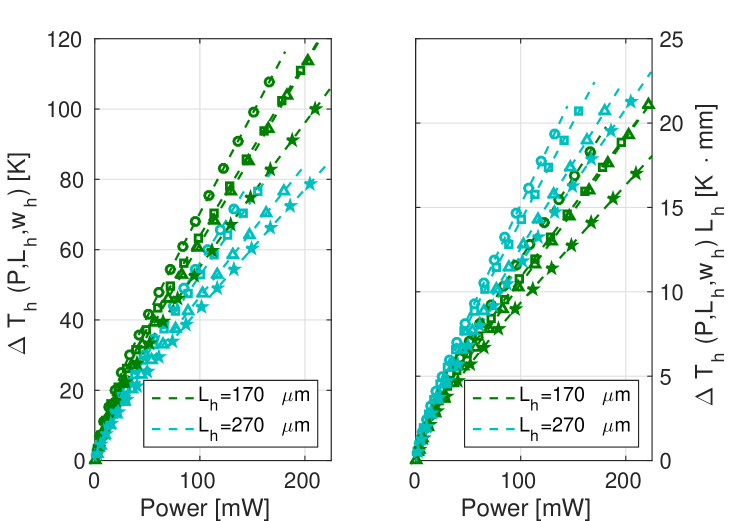
Resistivity is reported to grow with temperature [18] up to a point for which the heater structure is destroyed. Fig. 5 shows the thermal tuner resistance increase with driving power, for the different heater lengths on chip, and for widths m and m. This is connected to footprint and switching power in the next section.
4 Switching power
For a current flowing through the thermal tuner, the heater temperature is proportional to the current and the resistance. The heater is on top of an optical waveguide, and the heat will flow down towards the waveguide core. This is shown in Fig. 6. The heat will alter the refractive indices of both the waveguide core and cladding, resulting into a change in the waveguide mode effective index. Therefore, a change in the optical phase of the propagated light will be imposed, which can be expressed as:
| (4) |
where is the rate of change of the effective index vs the waveguide core temperature , is the core temperature change induced by a heater driven with power , and is the heater effective length where the temperate change takes place. Using two different software packages (PhoeniX OptoDesigner and COMSOL Multi Physics) with the material properties (Appendix B) and a waveguide cross-section for a strip waveguide (DEWVG), K-1 was obtained. Moreover, the heat transfer efficiency from the heater metal to the core of the waveguide (for this particular cross-section) was computed to be approximately of 58%. The data from the simulations was extracted in thermal steady state, and heat conduction was considered, since convection is negligible [19].
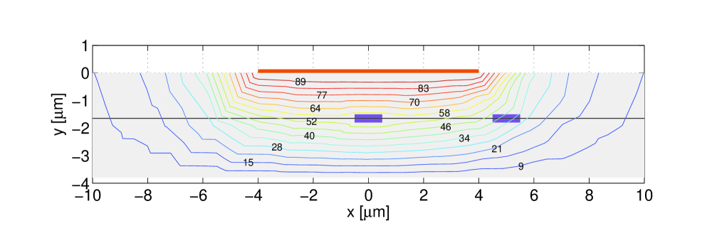
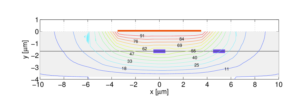
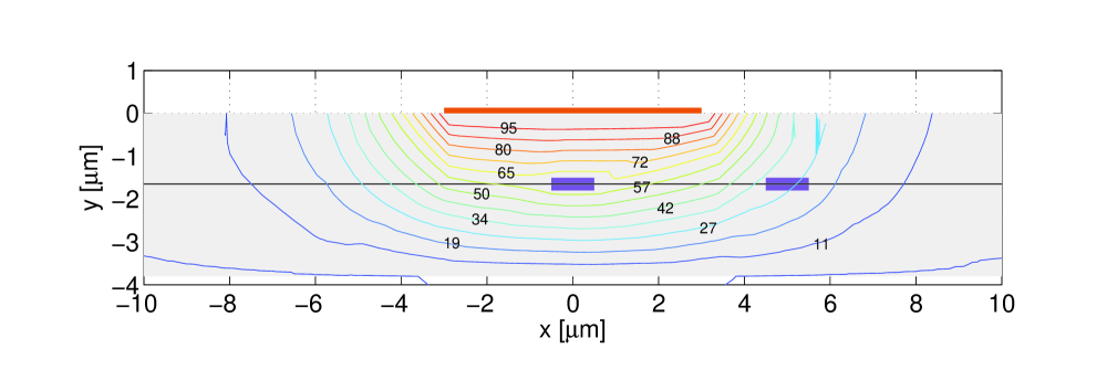
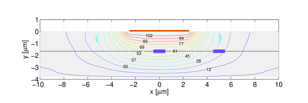
The heater dimensions influence on the temperature gradient that is created in the cross-section. For the same amount of heat, that is for the same amount of electric consumed power at the heater, , different temperature gradients result from heaters of different widths and lengths. This is stated explicitly as in eq. (4). In Fig. 6 four heaters with the same length, m, and widths of 5, 6, 7 and 8 m, are simulated for the same consumed power, with COMSOL MP software package. The silicon nitride waveguide, 1.0x0.3 m2 sits on top of 2 m of buried oxide, which in turn was grown on top of a silicon wafer of thickness 500 m. In the simulations, the temperature at the bottom part of the silicon is fixed to 25 ∘C. The voltage is set in the simulator for the wider heater ( m) to V, and owing to Fig. 4, the resistance is ( mW). For the narrow heaters, is set to provide the same power by using the resistance values from Fig. 6. The resulting temperature gradient in the core of the silicon nitride waveguide is approximately 11 ∘C more for the heater with narrower width. Hence, the same amount of heat is concentrated by narrow heaters, creating larger temperature gradients.
To infer more precisely on the variation of vs all the involved parameters, , , and , a multiparemeter sweep was performed using COMSOL MP, and the results are shown in Fig. 7. In the left panel, the results include the findings from Fig. 6, that is, for a fixed heater length (same line color) and same driving power, heaters with narrow width provide larger temperature gradients. Furthermore, the results for a fixed heater width (same symbols) show how, for a given driving power, increasing the length results into a redistribution of the driving power, and the local temperature increase is reduced. The latter, in terms of the accumulated phase shift (that is, ) is shown in the right panel within the same Fig. 7. As expected, the configuration with more accumulated temperature is that with the narrowest width, m, and longest length, m. However, this not surprising remark is not the most important message from this graph. Instead, the trade-off between local temperature increase vs. accumulated increase vs. footprint is the most noteworthy. Note this also in Fig. 7(b), how in terms of , the combinations of length width 270x8 m2 and 170x5 m2 are equivalent. But this is brought in relation to Fig. 5, since footprint reduction comes at the cost of higher increases resistance vs. power, and hence higher risk of damaging (burning) the thermal tuner.
As mentioned in the introduction, one figure typically employed to asses on the optical performance of the thermal tuner is the electrical power required for an optical phase change of , named . In order to derive the value from measurements, the optical spectral response for the MZIs having different tuner widths and lengths were recorded, for different input currents. The chip was held in a vacuum copper chuck, thermally stabilized to 25 ∘C. Light from a C-band broadband source NP Photonics ASE-CL-20-S was injected in the MZI, and the optical spectrum was recorded with an OSA, Yokogawa AQ6370C, with 10 pm resolution and sensitivity mode high. The asymmetric MZIs spectral response, with a path length difference of 622.38 m, have a Free Spectral Range (FSR) of 2 nm, for the waveguide cross-section group index . The spectral shifts for each drive current at the tuner were recorded, and from them, the corresponding phase shift derived, since for the MZI eq. (4) is related to the wavelength shift over the FSR as:
| (5) |
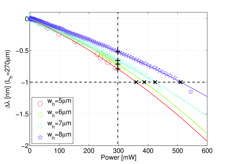
All the shifts below the OSA resolution were discarded. The results are shown in Fig. 8. Panel (a) shows the wavelength shift for different drive powers, using heaters of length 270 m and different widths. As previously illustrated in Fig. 6 reducing the width increases the temperature gradient, therefore less power is required to generate the amount of heat for the phase shift (horizontal dashed line, cross symbols). Analog, for a given drive power, the shift is always larger for narrow heaters, as marked with a vertical dash-dot line and plus signs. In particular, this vertical line is set to the power of 297.62 mW of Fig. 6. The wavelength shifts for widths from 5, 6, 7 and 8 m, are -0.7922, -0.7153, -0.6574, -0.5197 nm, respectively. Using the equations (4)-(5), the temperature changes in the core from Fig. 6, and K-1, the effective length over which the thermal effect takes place can be calculated with eq. (4). For this particular case, is 1.1834, 1.1220, 1.0667 and 0.9058 for widths from 5 to 8 m.
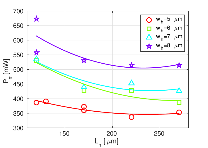
Finally, the results in Fig. 8(b) show how the estimated required increases progressively towards shorter heater lengths (smaller footprint). This is related to the effect of heat increasing the resistivity already discussed. Note that devices with lengths below 270 m were extremely unstable and tended to get burnt easily, therefore concluding a length of 270 m is safe in terms of heater resilience.
5 Thermal cross-talk
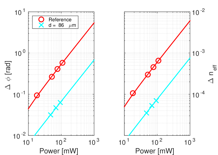
The heat generated by the thermal tuner of a MZI, propagates in the lateral direction and reaches other photonic devices on the chip, as can be also appreciated in Fig. 6. For long thermal tuners with wider tracks, i.e. small , no issues have been reported in the literature. The thermal cross-talk for nearby MZIs, Fig. 2 was investigated as follows: the thermal tuner of one MZI was biased and taken as reference, and the spectral traces recorded for both the biased MZI and the adjacent one. Once more from the spectral traces, the wavelength shifts were extracted. Then, owing to eq. (5) the wavelength shifts were translated into their corresponding phase shifts and effective index change. The results are shown in Fig. 9, log scale, along with linear fitting lines. They correspond to the pairs of MZIs in Fig. 2 labeled as 5, 10, 15 and 20. All these MZIs have heaters with m and m (compact and providing high . From the results, two conclusions are derived. Firstly and as expected, increasing the distance between reduces the amount of cross-talk. The distance required for an influence of less than one order of magnitude is above 20 m. Secondly, the relative distance between curves is constant with increasing powers, leading to the conclusion that the heat conduction through the materials is independent of the drive power.
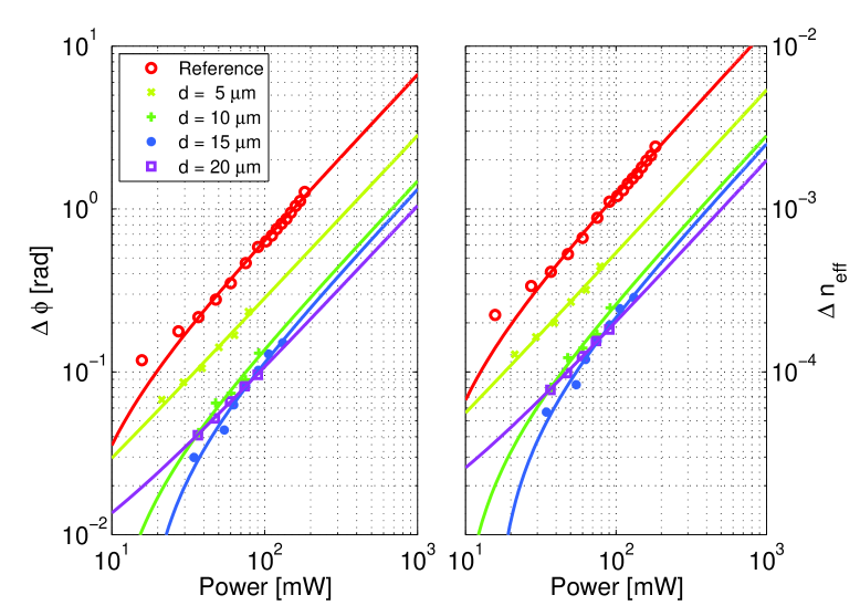
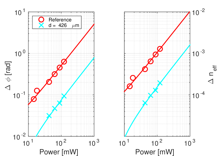
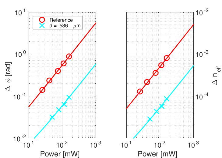
Albeit the chip layout was originally devised for the nearby cross-talk measurements shown, a few other structures allowed to perform similar measurements, for longer distances, labeled as , and in Fig. 2. The heaters in these structures have different widths and lengths of those in Fig. 9. Furthermore, as can be seen in Fig. 2, there is not only the Silicon Oxide cladding between the tuned and affected MZIs, but also some other Silicon Nitride waveguides run through. All this prevents from being able to directly compare (i.e. include in the same graph) all these results among them. This is also supported by the findings in section 4, where the dependence of the temperature gradient (and hence the associated effective index and phase change) with heater structural (width and length) and operational (power) parameters were reported. Despite all the above, the results are provided in standalone individual graphs per heater configuration in Fig. 10 as reference.
6 Discussion and outlook
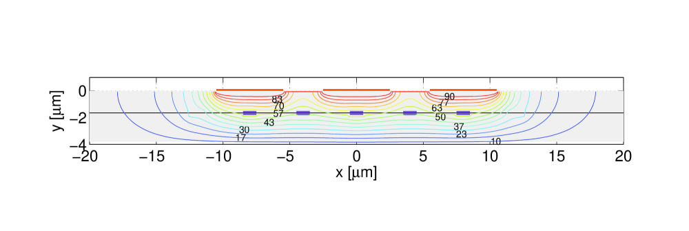
In terms of the heat generated by the thermal tuner, all except the local temperature gradient surrounding the waveguide core is lost. Therefore, it may be of interest to explore novel heater-waveguide configurations, which do not resort to additional process steps. Just as a proposal, Fig. 11 shows a cross-section with three metal stripes, and five cores beneath, corresponding to the same optical waveguide, which from top view perspective may be folded in different shapes such as spiral, serpentine or other. The dimensions and locations of the heaters and waveguides are engineered to fulfill two requirements. Firstly, the waveguides need to be placed apart a distance for which, when running in parallel, the optical cross-talk is negligible. In the picture, the waveguides are located at a distance of 4 m, which according to the technology employed results into negligible optical cross-talk for as much as 40 mm parallel running length. Secondly, for all the optical waveguides to be subject to exactly the same temperature gradient, their position, along with the heater width and spacing, needs to be engineered as well. The picture shows a line across the waveguide cores, wherein the temperature gradient is the same. Furthermore note how three heaters can be used in this configuration to tune over five sections of the same waveguide. Therefore this provides an increase in efficiency of five to three, with respect to the case of a single heater-waveguide configuration. The multi-heater-waveguide array may be of use in layouts where long tunable delays are required, and for which energy consumption is an issue [15]. All this results into a more efficient thermal tuner, since a) waveguide section in between heaters benefit from otherwise lost heat b) the heater is folded so is also longer, therefore requiring less power consumption for a targeted index change and c) the overall heater structure uses less temperature gradient, so the cross-talk towards non-targeted waveguides will be smaller.
7 Conclusions
The design trade-offs for the implementation of small footprint thermal tuners on silicon nitride have been presented. Test dies with Mach-Zehnder Interferometer test structure including compact thermal tuners of different dimensions were fabricated and tested, and the results were support with thermo-optic simulations. Compactness and thermal efficiency are traded off to heater deterioration and cross-talk. As path for improvement and future work, a multi-heater folded optical waveguide, where the number of heater stripes is less than the optical core cross-sections beneath, is proposed. Tuners with footprint of 270x5 m2 and switching power of 350 mW are reported among other, where the thermal-cross talk on dummy MZIs at distances over 20 m, in terms of induced phase change, is less than one order of magnitude of that of the tuned device.
Appendix A Resistance for a linearly tapered conductor
The resistance for a linearly tapered conductor is given by:
| (6) | |||||
Hence, and are given by:
| (7) |
| (8) |
Appendix B Summary of material properties
For the materials involved, the following parameters were used. Refractive indices:
| (9) |
| (10) |
Thermo-optic coefficients:
| (11) |
| (12) |
Thermal conductivity:
| (13) |
| (14) |
In COMSOL Multi-Physics, the measured resistivity reported in Section 3 was employed for the simulations.
Acknowledgment
The authors acknowledge financial support by: the Spanish CDTI NEOTEC start-up programme, the Spanish MINECO projects TEC2013-42332-P PIF4ESP, TEC2015-69787-REDT PIC4TB, and TEC2014-60378-C2-1-R MEMES, the GVA PROMETEO 2013/012 research excellency award, the EU H2020-ICT-27-2015 CSA Proposal number 687777, project FEDER UPVOV 10-3E-492 and project FEDER UPVOV 08-3E-008. D. Pérez acknowledges final support through the FPI grant programme by Universitat Politècnica de València.
References
- [1] A. E. Willner, R. L. Byer, C. J. Chang-Hasnain, S. R. Forrest, H. Kressel, H. Kogelnik, G. J. Tearney, C. H. Townes, and M. N. Zervas, “Optics and photonics: Key enabling technologies.” Proceedings of the IEEE, vol. 100, no. Centennial-Issue, pp. 1604–1643, 2012.
- [2] A. E.-J. Lim, J. Song, Q. Fang, C. Li, X. Tu, N. Duan, K. K. Chen, R. P.-C. Tern, and T.-Y. Liow, “Review of silicon photonics foundry efforts,” Selected Topics in Quantum Electronics, IEEE Journal of, vol. 20, no. 4, pp. 405–416, 2014.
- [3] M. Streshinsky, R. Ding, Y. Liu, A. Novack, C. Galland, A. E.-J. Lim, P. G.-Q. Lo, T. Baehr-Jones, and M. Hochberg, “The road to affordable, large-scale silicon photonics,” Opt. Photon. News, vol. 24, no. 9, pp. 32–39, Sep 2013. [Online]. Available: http://www.osa-opn.org/abstract.cfm?URI=opn-24-9-32
- [4] M. Smit, X. Leijtens, H. Ambrosius, E. Bente, J. Van der Tol, B. Smalbrugge, T. De Vries, E.-J. Geluk, J. Bolk, R. Van Veldhoven et al., “An introduction to inp-based generic integration technology,” Semiconductor Science and Technology, vol. 29, no. 8, p. 083001, 2014.
- [5] M. Smit and K. Williams, “Progress in inp-based photonic integration,” in Frontiers in Optics 2015. Optical Society of America, 2015, p. FW5B.4. [Online]. Available: http://www.osapublishing.org/abstract.cfm?URI=FiO-2015-FW5B.4
- [6] F. Kish, R. Nagarajan, D. Welch, P. Evans, J. Rossi, J. Pleumeekers, A. Dentai, M. Kato, S. Corzine, R. Muthiah et al., “From visible light-emitting diodes to large-scale iii–v photonic integrated circuits,” Proceedings of the IEEE, vol. 101, no. 10, pp. 2255–2270, 2013.
- [7] I. Garcés, F. Villuendas, J. A. Valles, C. Domínguez, and M. Moreno, “Analysis of leakage properties and guiding conditions of rib antiresonant reflecting optical waveguides,” Lightwave Technology, Journal of, vol. 14, no. 5, pp. 798–805, 1996.
- [8] E. Schipper, A. Brugman, C. Domínguez, L. M. Lechuga, R. Kooyman, and J. Greve, “The realization of an integrated mach-zehnder waveguide immunosensor in silicon technology,” Sensors and Actuators B: Chemical, vol. 40, no. 2, pp. 147–153, 1997.
- [9] A. Leinse, R. Heideman, M. Hoekman, F. Schreuder, F. Falke, C. Roeloffzen, L. Zhuang, M. Burla, D. Marpaung, D. Geuzebroek et al., “TriPleX waveguide platform: low-loss technology over a wide wavelength range,” in SPIE Microtechnologies. International Society for Optics and Photonics, 2013, pp. 87 670E–87 670E.
- [10] S. Romero-García, F. Merget, F. Zhong, H. Finkelstein, and J. Witzens, “Silicon nitride cmos-compatible platform for integrated photonics applications at visible wavelengths,” Opt. Express, vol. 21, no. 12, pp. 14 036–14 046, Jun 2013. [Online]. Available: http://www.opticsexpress.org/abstract.cfm?URI=oe-21-12-14036
- [11] D. Doménech, P. Muñoz, A. Sánchez, J. M. Cirera, and C. Domínguez, “Generic silicon nitride foundry development: Open access to low cost photonic integrated circuits prototyping,” in Opto-electronics Conference (OPTOEL). Salamanca (Spain), July 2015.
- [12] M. Nedeljkovic, R. Soref, and G. Z. Mashanovich, “Free-carrier electrorefraction and electroabsorption modulation predictions for silicon over the 1–14-infrared wavelength range,” Photonics Journal, IEEE, vol. 3, no. 6, pp. 1171–1180, 2011.
- [13] N. Hosseini, R. Dekker, M. Hoekman, M. Dekkers, J. Bos, A. Leinse, and R. Heideman, “Stress-optic modulator in TriPleX platform using a piezoelectric lead zirconate titanate (pzt) thin film,” Optics express, vol. 23, no. 11, pp. 14 018–14 026, 2015.
- [14] G. Gilardi, W. Yao, H. R. Haghighi, X. J. Leijtens, M. K. Smit, and M. Wale, “Deep trenches for thermal crosstalk reduction in inp-based photonic integrated circuits,” Journal of Lightwave Technology, vol. 32, no. 24, pp. 4262–4268, 2014.
- [15] C. G. Roeloffzen, L. Zhuang, C. Taddei, A. Leinse, R. G. Heideman, P. W. van Dijk, R. M. Oldenbeuving, D. A. Marpaung, M. Burla, and K.-J. Boller, “Silicon nitride microwave photonic circuits,” Optics express, vol. 21, no. 19, pp. 22 937–22 961, 2013.
- [16] M. S. Hai, A. Leinse, T. Veenstra, and O. Liboiron-Ladouceur, “A thermally tunable 14 channel wavelength demultiplexer designed on a low-loss si3n4 waveguide platform,” in Photonics, vol. 2, no. 4. Multidisciplinary Digital Publishing Institute, 2015, pp. 1065–1080.
- [17] H.-W. Chen, A. W. Fang, J. D. Peters, Z. Wang, J. Bovington, D. Liang, and J. E. Bowers, “Integrated microwave photonic filter on a hybrid silicon platform,” Microwave Theory and Techniques, IEEE Transactions on, vol. 58, no. 11, pp. 3213–3219, 2010.
- [18] R. A. Matula, “Electrical resistivity of copper, gold, palladium, and silver,” Journal of Physical and Chemical Reference Data, vol. 8, no. 4, 1979.
- [19] T. L. Bergman, F. P. Incropera, and A. S. Lavine, Fundamentals of heat and mass transfer. John Wiley & Sons, 2011.