From vertex detectors to inner trackers with CMOS pixel sensors
Abstract
The use of CMOS Pixel Sensors (CPS) for high resolution and low material vertex detectors has been validated with the 2014 and 2015 physics runs of the STAR-PXL detector at RHIC/BNL. This opens the door to the use of CPS for inner tracking devices, with 10-100 times larger sensitive area, which require therefore a sensor design privileging power saving, response uniformity and robustness. The CMOS technology used for the STAR-PXL sensors was considered as too poorly suited to upcoming applications like the upgraded ALICE Inner Tracking System (ITS), which requires sensors with one order of magnitude improvement on readout speed and improved radiation tolerance. This triggered the exploration of a deeper sub-micron CMOS technology, Tower-Jazz , for the design of a CPS well adapted for the new ALICE-ITS running conditions. This paper reports the R&D results for the conception of a CPS well adapted for the ALICE-ITS.
keywords:
CMOS sensors, vertex detector, tracker1 Introduction
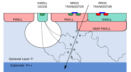
CPS integrate on the same silicon substrate the sensing elements and the front-end and readout circuitry (c.f. Fig. 1). Impinging charged particles create electron-hole pairs in a moderately P-doped epitaxial layer located on top of a highly P-doped (P++) wafer substrate and below some highly doped P-well (P++) implants of the front-end circuitry. The generated electrons are collected on a N-well implanted on top of the epitaxial layer. In conventional CPS, the epitaxial layer is not fully depleted, and the electrons move mainly by thermal diffusion. However, they are deflected by build-in voltages of the P-epi/P++ interfaces which somewhat guide them toward the N-well/P-epi collection diode. Once collected, the charge is stored in the diode-parasitic capacitance, which voltage drop is amplified by a low-noise in-pixel amplifier.
CPS feature the possibility of fine pixel pitch (down to ) providing a very good spatial resolution (typically a few ). The very thin epitaxial layer () allows to thin the sensor down to , which turns into an exceptionally small material budget. Furthermore, the sensors can be operated at room temperature, avoiding to use complicated cooling systems which additionally contribute to the material budget.
| STAR-PXL | ITS (in) | ITS (out) | |
|---|---|---|---|
| TID | |||
| NIEL | |||
| Power | |||
| Surface to cover |
A competitive tolerance to non-ionizing radiation (up to ) was achieved when CMOS-processes with lightly-doped (so-called high-resistivity) epitaxial layer became available. This improved significantly the depletion depth up to several , dramatically accelerating the charge collection, an thus reducing the transit time around trapping-defects in the bulk generated by non-ionizing radiation.
| MIMOSA-28 | FSBB-M0 | Mi-22THRb | MISTRAL-O | |
|---|---|---|---|---|
| CMOS process | ||||
| Pixels (col.row) | ||||
| Pixel pitch [] | or | |||
| Sensitive area [] | ||||
| [] | ||||
| [] | ||||
| TID [] | ||||
| NIEL [] | ||||
| Power [] | N/A | |||
| Pads over pixels | No | No | Yes | Yes |
| On-chip sparsification | 1D | 2D | None | 2D |
The sensor’s readout speed depends on the on-chip data processing circuitry. Initially, the signal from the in-pixel amplifier was multiplexed to a common analog readout bus and sent out for further processing, giving a few readout time () for a sensor of larger sensitive area. A factor of 1000 reduction in was obtained by reading in succession rows of the pixel matrix, allowing each pixel to send in parallel their signal to the column end, the so-called rolling shutter architecture. This data is then processed trough discriminators ending each column for digitization and then further processed by an on-chip data sparsification circuit. This allowed parallel column readout and reduced transmission band-width, shortening the to about .
All these developments allowed the conception of a CPS, called MIMOSA-28 [1] (c.f. table 2), suited to the STAR-PXL detector [2] operated at RHIC/BNL, the first vertex detector based on the CPS technology. The STAR-PXL has successfully participated to two data-taking campaigns and is currently in operation. It has proven to be reliable and to deliver the expected added value for the STAR physics program. The 400 sensors composing the PXL have allowed accumulating a sizable amount of experience with these devices.
The performances reached by the MIMOSA-28 sensor are not suited to match some of the more demanding requirements of the new ALICE-ITS [3] (c.f. table 1), mainly in terms of and power consumption (outer layers), and to a lesser extent in terms of radiation tolerance 111The ALICE-ITS doses in table 1 are the ones reported in the TDR, but more detailed studies have shown that significantly lower doses need to be tolerated. (inner layers). This triggered the exploration of a new CMOS process with several advantages to overcome the limitations of the AMS CMOS process used for MIMOSA-28. This document describes the features of the new CMOS process and its advantages as compared to elder ones. Furthermore, current status of the R&D for the conception of a sensor adapted for the ALICE-ITS outer layers is also presented.
2 ALICE-ITS upgrade: R&D of sensors for outer layers
To overcome the limitations of the MIMOSA-28 sensor for the ALICE-ITS application, it was decided to migrate to the novel Tower-Jazz CMOS process. One of its aspects is the smaller feature size, improving the (higher integration density) and tolerance to ionizing radiation. Furthermore, the process grants thicker epitaxial layers with higher resistivity, improving the signal-to-noise ratio and tolerance to non-ionizing radiation. Finally, the new technology concedes for deep P-well implants which shield the N-well hosting PMOS transistors, preventing parasitic charge collection. This allows both PMOS and NMOS transistors to be used inside pixels, permitting to implement an in-pixel discriminator.
All these features widen the choice of the readout architecture strategy. An asynchronous readout similar to the one used for the hybrid pixel sensors [4] is pursued via the ALPIDE design [5], which is the most promising approach to equip the ALICE-ITS inner layers. This approach comes with certain risks of missing the project’s tight schedule, as it requires building and testing a complex pixel matrix with several new features to be validated. In order to be on schedule it was decided to also follow a more conservative approach, the MISTRAL-O chip, using the validated rolling shutter readout of the MIMOSA-28 sensor. MISTRAL-O was intended to instrument the ALICE-ITS outer layers, which feature two orders of magnitude higher surface to cover, thus requiring special attention on power consumption, response uniformity and robustness.
MISTRAL-O needs to be about 10 times faster than MIMOSA-28 together with twice less power consumption (c.f. table 1). It has as well to be pin-to-pin compatible with the ALPIDE design, which includes pads over the pixel matrix suited to laser soldering. Furthermore, the sensor’s slow control and digital logic need to be adapted to ALPIDE’s standards.
2.1 Rolling shutter readout in the novel CMOS-process
As a first step for validating the new CMOS-process, a full scale prototype called FSBB-M0 was built early in 2015 (c.f. table 2). The sensor includes a very similar analog front-end and digital readout chain as the MIMOSA-28 sensor with a reduced by a factor of . This was achieved by reducing the number of pixels in a column to be readout () and increasing the size of the pixel long the column (). Furthermore, the rolling shutter readout mode addresses simultaneously all pixels belonging to a pair of neighboring rows. Therefore, each discriminator addresses 208 pixels instead of 928, with a proportionnally reduced . The sensing nodes are staggered in order to maximize the uniformity of the sensing node density and to alleviate the spatial resolution asymmetry consecutive to the pixel’s rectangular shape. Moreover, the sparsification circuit allows to find clusters of pixels in 2-dimensional windows instead of the 1-dimensional ones of MIMOSA-28, which had to be merged off-line.
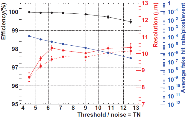
Several FSBB-M0 sensors were first studied in the laboratory, where their temporal and fixed pattern noise performances were assessed over a wide range of positive temperatures. These measurements were performed before and after irradiation with an X-Ray source (up to ) and with neutrons (up to ), up to doses relevant for the ALICE-ITS inner layers (c.f. table 1). The sensors were next tested with particle beams at the CERN-SPS with negatively charger pions of , and at DESY with electrons of . Each set-up was made of six FSBB-M0 sensors operated simultaneously on beam. The performances of each sensor were assessed by considering it as a Device Under Test (DUT) and the rest as reference planes for track reconstruction (telescope). The measurements showed satisfactory results, ilustrated by Fig. 2. A nearly detection efficiency and a dark occupancy of was observed for all non-irradiated sensors tested. The dark occupancy could be reduced by an order of magnitude by masking a small fraction () of the noisiest pixels, with negligible impact on the detection efficiency. Satisfactory detection efficiency () was also obtained for sensors irradiated at doses relevant for the ALICE-ITS inner layers, and dark occupancies of were obtained by masking the noisiest pixels.
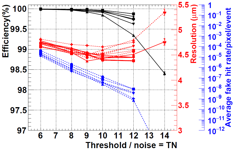
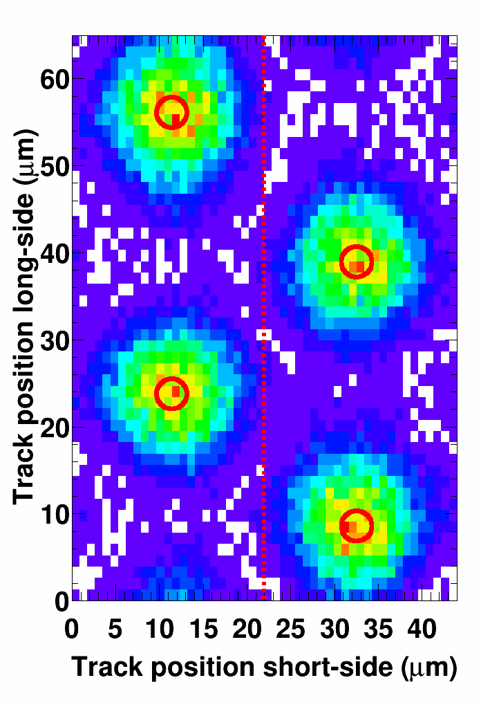
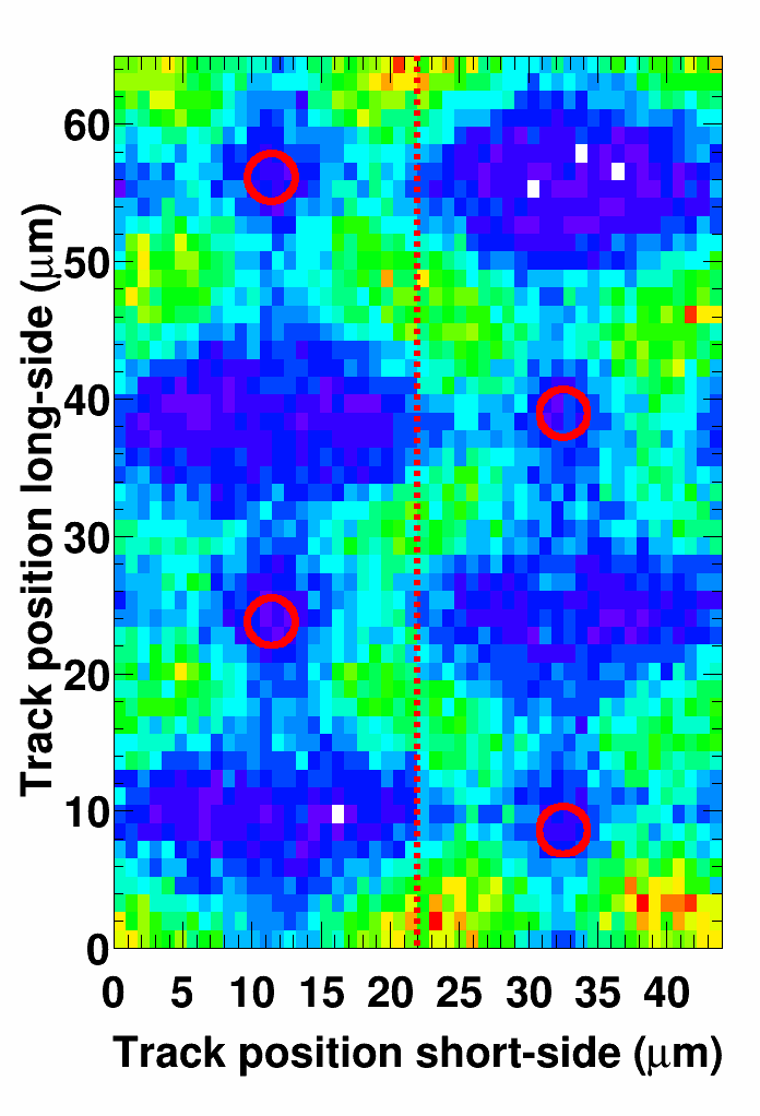
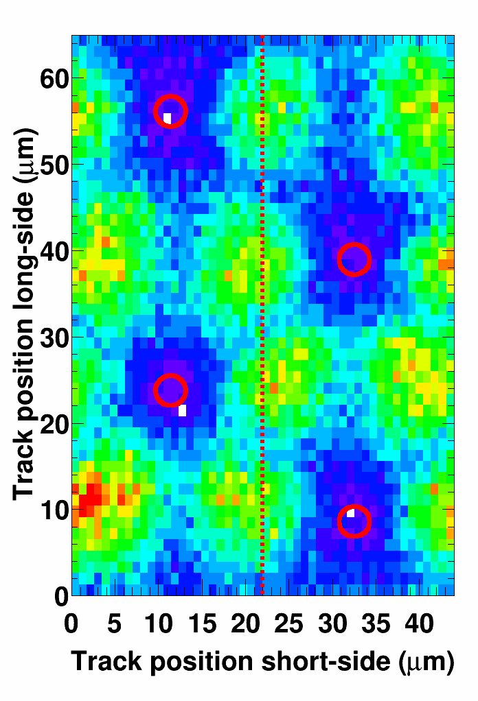
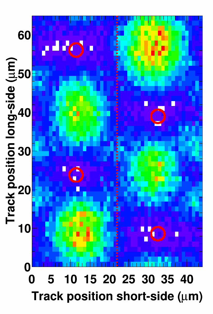
In order to estimate the telescope pointing resolution () at the DUT position, the experimental set-up was simulated with a Geant4-based tool. A from to ( to ), was obtained at the CERN-SPS (DESY) beam test facility. The low (high) values of correspond to the DUT located at the center (ends) of the sensors layout. This allowed to estimate the DUT spatial resolution () by subtracting the from the track-hit residue. As shown in Fig. 2, a of was obtained for all six sensors tested, with a slightly higher value along the long-side of the rectangular pixel (). It is substantially better than one would expect for the digital readout according to the rule. This follows from charge charing, giving a hit pixel multiplicity of about 3 in average, thereby providing a substantially better based on the center-of-gravity of the cluster of pixels. The sensitivity of to charge sharing is shown in Fig. 3, which displays, for different hit pixel multiplicities, the tracks impact position with respect to the closest collection diode. One can appreciate the regions with respect to the collection diodes where an impinging particle needs to hit the sensor in order to produce a given pixel multiplicity. The sizes of those regions give a measurement of the spatial resolution, which vary smoothly from one hit pixel multiplicity to the other. Even if a subset of about of the hits show only one pixel, they exhibit a much better than in both pixel directions. Such single pixel clusters are formed exclusively by particles impinging the pixel near the collection diode (top-left plot of Fig. 3), otherwise clusters include systematically more than one pixel.
2.2 Large pixel design and validation
The observed detection performances of the FSBB-M0 prototype validated the implementation of the rolling shutter architecture with the new CMOS-process. The next step consisted in addressing the ALICE-ITS requirements by achieving nearly twice less readout time and power consumption. A large fraction of the power consumption is due to the in-pixel circuitry. Power savings can then be achieved by minimizing the number of pixels per sensor, i.e. by increasing their dimensions. This approach exploited the alleviated spatial resolution requirement for the outer layers as compared to the inner layers (c.f. table 1). Furthermore, the use of large pixels elongated in the row direction further downscales the number of pixels per discriminator and the number of columns per surface unit, reducing in this way the and the power consumption. The increase of the pixel surface has however drawbacks in terms of charge collection. The mean distance the signal charges cross until being collected increases as the collection diode density is reduced, increasing the probability for charge trapping by defects of the silicon crystalline structure. This probability is further enhanced after non-ionizing irradiation. However, this effect is foreseen to remain acceptable given the relaxed requirements in the ALICE-ITS outer layers.
CPS exploring large pixel detection properties (Mi-22THRb, c.f. table 2) were manufactured in 2014 in the Tower-Jazz CMOS process featuring 6 metalization layers and deep P-wells implants. Two different pixel dimensions of and were implemented. Each pixel incorporates a sensing node connected to a pre-amplifier featuring a feedback loop ended with a forward biased diode compensating the leakage current delivered by the sensing node and fixing its depletion voltage. The preamplifier is followed by a clamping circuit subtracting the pixel pedestal and connected to a discriminator located at the column end. The sensing nodes are staggered in order to maximize the uniformity of the sensing node density and to alleviate the spatial resolution asymmetry consecutive to the pixel’s rectangular shape. The matrix, made of 64 columns of 64 pixels, is read out in rolling shutter mode addressing simultaneously all pixels belonging to a pair of neighboring rows. 8 columns feature (discriminator free) analog output for pixel circuitry assessment purposes. The of the sensor is .
The relatively large pixel size allows to integrate in-pixel circuitry for noisy pixel masking. Furthermore, the dimensions enable to concentrate the in-pixel circuitry within 3 metalization layers only. This allows integrating connection pads over the pixel array, using the two top metal layers. In the MIMOSA-28 sensor, a MIM (Metal-Insulator-Metal) clamping capacitor was implemented using the two top metalization layers. The connection pads over the pixel array forced to explore new alternatives of the clamping capacitor implementation.
The prototyping of the large pixel concept addressed in particular the detection efficiency, the spatial resolution, the radiation tolerance and the in-pixel circuitry with a new clamping design. For this purpose, several pixel variants were designed and implemented in 8 different pixel arrays, including a reference one based on 6 metalization layers.
The sensors were first studied in the laboratory, where their temporal and fixed pattern noise performances were assessed over a wide range of positive temperatures and where their response to an source were studied and used to calibrate the charge-to-voltage conversion gain; these measurements were performed before and after irradiation with an X-Ray source (up to ) and with neutrons (up to ), up to doses relevant for the ALICE-ITS outer layers. The sensors were next tested on an electron beam of at the Frascati beam test facility (LNF/BTF) [6]. A telescope composed of analog output sensors (MIMOSA-18 [7]) featuring a spatial resolution were used to predict the beam particle impact position at the DUT (Mi-22THRb sensors) location. The telescope was simulated in detail, accounting for multiple scattering. The predicted telescope pointing resolution amounts to . Fig. 4 shows a representative result of this beam test. For both pixel dimensions, a nearly detection efficiency was observed for non-irradiated sensors. Satisfactory detection efficiency () was also obtained for sensors irradiated at doses relevant of the ALICE-ITS outer layers. Moreover, a spatial resolution of in both directions was found for all pixel variants tested. All these results comply with all ambitioned performances of the large pixel design well adapted for the ALICE-ITS outer layers (c.f. table 1).
3 Summary and outlook
This paper summarizes the R&D results for the design of a CPS well adapted to the ALICE-ITS outer layers. Two prototypes were fabricated and fully tested. The first one addressed the validation of the rolling shutter readout architecture implemented in the new Tower-Jazz CMOS-process, with nearly four times shorter than the MIMOSA-28 sensor equipping the STAR-PXL. The second prototype addressed a large pixel design, including bonding pads over the pixel matrix, to further squeeze and the power consumption, while complying with and radiation hardness requirements of the ALICE-ITS outer layers. The results obtained validate the possibility to fabricate the MISTRAL-O sensor (c.f. table 2), featuring pixels over of sensitive area, a and dissipating less than , well within the target requirements (c.f. table 1).
The results presented in this paper validate the Tower-Jazz CMOS technology, as well as the strategies for improving the readout speed, power consumption and radiation tolerance for future applications. Among them the vertex detector (MVD) of the forthcoming CBM experiment [8] at FAIR/GSI and a vertex detector suited to experiments foreseen at the ILC [9].
Acknowledgements
We thank our colleagues C. Bedda and I. Ravasenga (INFN-Torino), and P. La Rocca and F. Riggi (INFN-Catania), for their contributions to the beam test of Mi-22THRb at LNF/BTF.
References
- [1] C. Hu-Guo et al., Design and characterization of a fast architecture providing zero suppressed digital output integrated in a high resolution CMOS pixel sensor for the STAR vertex detector and the EUDET beam telescope, TWEPP, Naxos, Greece, September 2008, CERN-2008-008.
- [2] J. Schambach et al., A MAPS Based Micro-Vertex Detector for the STAR Experiment, Physics Procedia 66 (2015) 514-519.
- [3] B. Abelev et al. (The ALICE Collaboration), Technical Design Report for the Upgrade of the ALICE Inner Tracking System, 2014 J. Phys. G: Nucl. Part. Phys. 41 087002. doi:10.1088/0954-3899/41/8/087002.
- [4] M. Garcia-Sciveres et al., The FE-I4 pixel readout integrated circuit, NIM-A Volume 636, Issue 1, Supplement, 21 April 2011, Pages S155-S159.
- [5] G. Aglieri Rinella, these proceedings.
- [6] B. Buonomo et al., Performance and upgrade of the DAPHNE Beam Test Facility (BTF), IEEE Trans. Nucl. Sci. 52 (2005) 824.
- [7] W. Dulinski et al., Beam telescope for medium energy particles based on thin sub-micron precision MAPS DOC, IEEE Nuclear Science Symposium 2007, Hawai (October 27, November 3).
- [8] M. Deveaux et al., The silicon detector systems of the Compressed Baryonic Matter experiment, POS(Vertex 2013) 009.
- [9] Ties Behnke et al., The International Linear Collider Technical Design Report - Volume 4: Detectors, arXiv:1306.6329 [physics.ins-det].