Bianisotropy and magnetism in plasmonic gratings
Abstract
We present a simple design to achieve bianisotropy at visible wavelengths: an ultrathin plasmonic grating made of a gold grating covered by a thin flat layer of gold. We show experimentally and through simulations that the grating exhibits magneto-electric coupling and features asymmetric reflection and absorption, all that with a device thickness of a tenth of the operating wavelength. We compared the spectral results and retrieved the effective material parameters of different polarizations and devices. We show that both asymmetry and strong coupling between the incoming light and the optically interacting surfaces are required for obtaining asymmetric optical behavior in metasurfaces.
keywords:
Bianisotropy, Magnetism, Plasmonics, Grating, MetamaterialThese authors contributed equally Imperial College London]Blackett Laboratory, Department of Physics, Imperial College London, London SW7 2AZ, United Kingdom \altaffiliationThese authors contributed equally Imperial College London]Blackett Laboratory, Department of Physics, Imperial College London, London SW7 2AZ, United Kingdom Nanyang Technological University]School of Electrical and Electronic Engineering, Nanyang Technological University, Nanyang Avenue 639798, Singapore Imperial College London]Blackett Laboratory, Department of Physics, Imperial College London, London SW7 2AZ, United Kingdom Imperial College London]Blackett Laboratory, Department of Physics, Imperial College London, London SW7 2AZ, United Kingdom
1 Introduction
In their seminal book 1, Landau and Lifshitz commented on the
insignificance of magnetism at optical frequencies. Yet, several recent studies have
shown that magnetic effects are present in optical systems 2, 3, 4 particularly those containing metals that have been
structured in some way. The mechanism is familiar from the concept of
metamaterials whereby novel electrical and magnetic properties can be found by
engineering the microstructure
5, 6, 7, 8. Here
we present an experimental study of a structured system, in our case a grating,
and interpret the data in terms of effective parameters of an equivalent
ultrathin layer of metamaterial. Features such as asymmetric reflection will emerge
from the interplay of magnetic and electric fields.
Lately, a lot of attention has been given to the development of metasurfaces –
textured surfaces at a sub-wavelength scale with tailored electro-magnetic
properties 9, 10, 11, 12, 13, 14. These devices are the two-dimensional counterpart of
metamaterials and benefit from the advantages of reduced profile, reduced ohmic and magnetic losses, and
simpler fabrication processes, thus enabling a range of applications from analogue computing 15, to ‘flat optics’ 16 and light harvesting applications 17, 18, to name a few.
A special class of metasurfaces comprises bianisotropic ones, that is, materials exhibiting coupling between the electric and magnetic fields 19, 20, 21, 22, which are described by the constitutive relations 19: and (see methods), with the coupling parameters and relating the displacement current (D) with the magnetic field (H), and the magnetic flux density (B) with the electrical field (E), respectively. A typical characteristic of bianisotropic structures is their asymmetric response depending on which side of the structure they are being probed from. 23
There is a large body of literature, discussing bianisotropy in the THz 21, 24 and GHz regimes25, 26, 27, 28, with applications in polarization changers
27, 29, asymmetric absorbers/reflectors 25, 28 and perfect absorbers 30.
However, in the spectral optical regime, very few experimental studies exists 29, 31, 32.
Recently, an asymmetric absorber operating in the visible frequency range has
been designed 32, where the asymmetry originates from a
dielectric-metal stack of thin a Ag nano-holes array patterned over a Silicon-Nitride membrane.
In this paper we show experimentally that asymmetric reflection
based on bianisotropy and magneto-electric coupling can be achieved at visible
wavelengths simply, using all-metal plasmonic gratings with reduced thickness of the
active region, in a design that requires simple and commonly used fabrication methods. Electrodynamic simulations are
compared with experimental results and are interpreted in terms of the
effective material parameters of the system, which clearly indicate magneto-electric coupling.
2 Results and discussion
Our bianisotropic metamaterial structure is made of metallic grating lines and a
thin conducting layer covering the grating lines and the spacing between them.
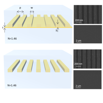
Figure 1 illustrates the bianisotropic structure
– 80m80m arrays of a 50nm thick gold grating covered by 10nm
layer of gold – next to a ‘control’ structure with a similar grating array, but lacking the thin gold
layer. The two types of gold structures were fabricated by means of electron beam
lithography and thermal evaporation on the same quartz substrate. Finally, in order
to limit asymmetries in the device only to the active metallic gratings
(and not to the substrate, for example) the device was completed by the bonding of
another quartz slab on top of the structures (see Methods for fabrication details).
2.1 Reflection and Transmission spectra
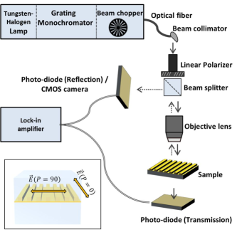
The reflection and transmission spectra of the two types of structures were
obtained using a setup of an optical microscope coupled to a grating
spectrometer for two linear polarizations: one for which the electric field is
aligned with the grating lines () and one where the polarization is
orthogonal to the gratings lines ().
For both simulations and measurements the plane
wave is normally incident (note that in our experiments, though centered around
the normal to the plane of the gratings, the plane wave is distributed throughout the
numerical aperture of the objective (N=0.5)). The recording of the transmitted
and reflected light was completed via Si photo-diodes coupled to a lock-in amplifier
(Figure 2; see Methods for detailed information about the
measurements set-up).
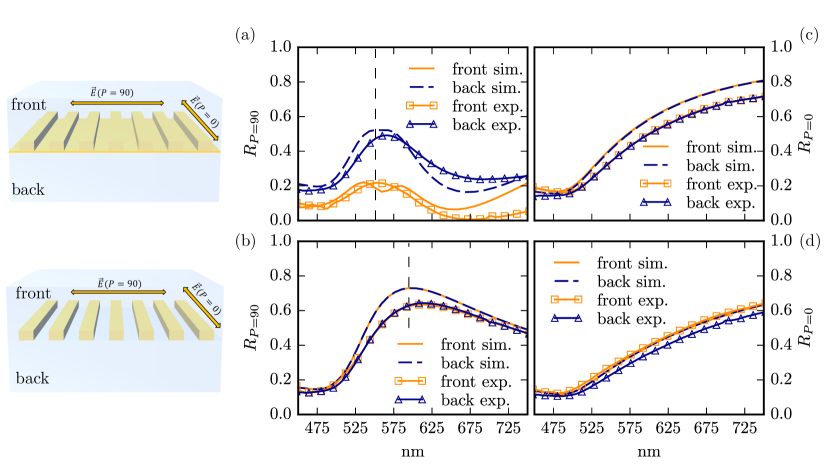
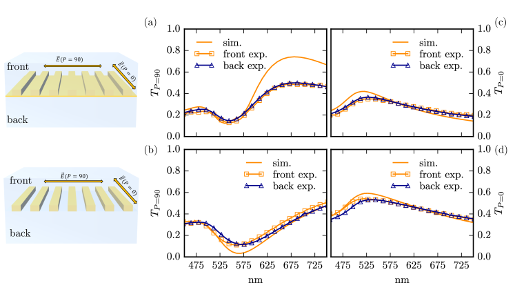
Figure 3 shows the experimental and simulated reflectance spectra for the bianisotropic and the control structures. For polarized light with its electric field orthogonal to the grating lines it shows a remarkable difference between the control sample with the metal gratings only, and the bianisotropic sample with the additional thin layer of gold: while the reflection spectra of the control structure (Figure 3c) are inherently indifferent to the direction of incoming light, as expected from an optically symmetric structure, the reflection signal of the gold grating with the additional thin gold layer (Figure 3a ) is up to 3 times stronger when the device is probed from the side of the thin-film (aka, ‘back exposure’), compared to probing from the corrugated side (’front exposure’). For this polarization of the electrical field the bianisotropic and the control devices show a plasmon resonance with maximal reflection at 550nm and 595nm, respectively – indicating strong coupling to the incident light. When probing the metal grating with the electrical field polarized along the grating lines, (Figure 3b and d), both the plasmon resonance and the asymmetric reflection diminishes, and we are left with a reflection curve akin to that of a planar Au layer. Unlike the reflection spectra, the transmission curve (Figure 4) is independent of the illumination direction, regardless to structure and polarization, as it must be due to reciprocity. For all structures and polarizations we see a qualitative agreement between experimental and numerical results with quantitative differences arising most likely from fabrication imperfections and uncertainties in the value of the permittivity.
It appears that an asymmetric reflection from our low profile structures is evident when the following two conditions are satisfied simultaneously: a) the device has to bear some optical asymmetry, and b) the incoming light has to be strongly coupled to, and absorbed by the active part of the device – here, achieved by means of plasmonic coupling between the incident light and the grating, when probed with the appropriate polarization. It is worth noting that, in bulk materials and structures, an optical asymmetry – and therefore asymmetric reflection – is abundant in nature and our daily life. Take for example a single side polished Silicon wafer, or a common bathroom mirror; both meet the former condition above and demonstrate asymmetric reflection with one side reflecting more than the other. However, while the asymmetric reflection in the case of the two macroscopic examples given above is due to their two dissimilar non-interacting surfaces, achieving asymmetric reflection while maintaining a low structure profile at the order of /10, as demonstrated here, requires a design which meets also the second condition of strong coupling between the incoming light and the optically interacting surfaces.
As asymmetric reflection could only be observed for the grating with the 10nm connecting layer of gold, it is clear that understanding the role of the thin conducting layer is crucial for the understanding of the origin of the asymmetric reflection: the conductive layer electrically connects neighboring grating lines, therefor enabling a flow of electrical current in the direction normal to the grating lines (P=90). The induced current, in turn, generates a magnetic field 33 radiating energy into the far field and interfering with the incident wave. This effect is enhanced via a plasmon resonance, as more energy is coupled into the grating. However, the structural asymmetry leads to different coupling strengths for front or back illumination. If the light is incident on the flat side, the surface does not immediately provide the missing momentum to couple to plasmons so that a large fraction of the light is reflected. On the corrugated side, the surface immediately provides the missing momentum and coupling into plasmons is more efficient leading to higher absorption and thus reduced reflection properties. This behavior is well known from bianisotropic bulk materials exhibiting magneto-electric coupling 19, 23. In order to further investigate the magneto-electric coupling and quantify its strength, we continue by modeling our meta-surface as a bianisotropic metamaterial 19, 23.
2.2 Effective material parameters and bianisotropy
An asymmetric reflection/absorption spectrum cannot be described by a
homogeneous slab model using effective permittivity and permeability
alone; instead, magneto-electric coupling has to be introduced to the physical
model by modifying the constitutive relations 19, 23, 21. The magneto-electric coupling is quantified by new material
parameters, and (see introduction and
section 4.2), which make the electric and magnetic fields
interact in a way such that even a symmetric slab exhibits asymmetric
reflection 19, 23, 21.
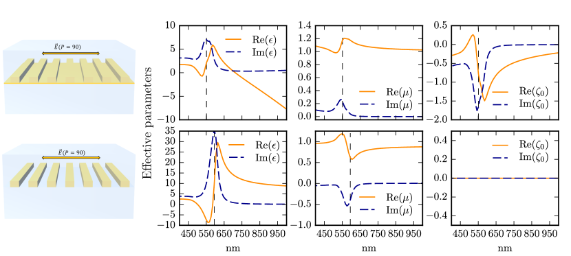
We model our connected grating as a homogeneous bianisotropic slab and compare against the control grating. Note that the magneto-electric coupling parameters and are determined by a single parameter , on which we focus hereafter. Figure 5 shows the material parameters retrieved from simulations of the types of gold gratings structures for . Clearly, the interplay of plasmon resonance and structural asymmetry in the connected gold grating lead to an induced magneto-electric effect, as demonstrated by the strong resonance in the coupling parameter . The control grating, however, shows no such coupling, highlighting the importance of that thin connecting Au layer for the design. Figure 5 exhibits two additional differences between the bianisotropic and control gratings. First, though both samples feature optical magnetic effects (resonant permeability) at the plasmon resonance, the permeability of the control grating does not return to unity in the long wavelength limit, but remains weakly diamagnetic. This seemingly counter-intuitive result is explained as follows. In the long wavelength limit, gold approaches a perfect conductor, thus expelling part of the magnetic field from its interior. This results in ‘squeezing’ of the magnetic field lines through the gaps of the grating, leading to the diamagnetic effect observed 35.The smaller the gap, the stronger this effect (see figure S3 in the supplementary material).
The case of the bi-anisotropic sample with the connected grating is understood by analogy with a superconductor where the permeability is unity, but the permittivity diverges inversely as the frequency squared. In this case magnetic fields are expelled entirely through the action of the permittivity, contrary to some misinformed statements to the effect that superconductors are perfect diamagnets. In figure 5 top left we see that for the continuously connected sample the effective permittivity diverges at long wavelengths.
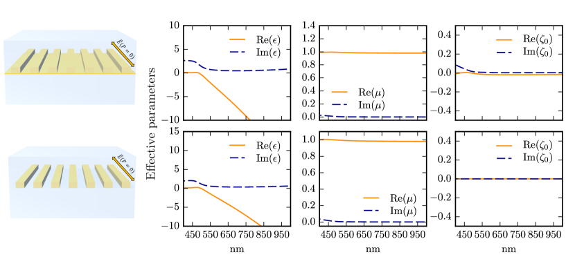
In figure 6 we look at the effective material parameters for . Here, the electric field is polarized along the grating lines and current can flow freely in both the control and bi-anisotropic gratings, similar to the current flow in thin gold films. The lack of a plasmon resonance leads to a near-zero magneto-electric coupling for the connected gold grating and the reflection spectra only shows minor deviations at short wavelengths at the order of the grating period.
3 Conclusion
We demonstrated experimentally and through simulations that plasmonic gratings provide a simple design for asymmetric reflectors/absorbers at visible wavelengths. We found that the asymmetry in the spectra is a direct consequence of magneto-electric coupling in the grating, i.e. bianisotropy, and should be interpreted as such. The strength of the bianisotropy provides a good measure for the expected asymmetry in the spectra and may be used for the optimization of this effect, as has been done at much lower frequencies previously 25. Finally, the bianisotropy of our grating is inherent to it, rather than induced by a substrate 32, which leads to an extremely small footprint of the structure ( thickness). Further optimizations in the grating design and fabrication are certain to enhance the strength of the asymmetry.
4 Methods
4.1 Experimental setup and fabrication
Fabrication of gratings structures: First, quartz substrates were cleaned by ultrasonic agitation in an acetone bath, followed up by IPA and DIW rinse. A Polymethyl methacrylate (PMMA 950, A4) positive resist spun on the cleaned substrates at 3500RPM for 60 seconds, and soft-baked on a hotplate at 180 C for 60 seconds, forming a 250 nm lift-off mask. Multiple arrays of grating lines were defined using a Raith eline Electron Beam Lithography tool at 10 kV accelerating voltage and 10 micro-meter aperture, and developed for 30 seconds in 1:3 methyl isobutyl ketone:isopropyl alcohol (MIBK:IPA) developer. Prior to the deposition of gold grating lines, the surface was modified to improve the adhesion of gold to the SiO2 substrate: a drop of (3-aminopropyl)triethoxysilane diluted in ethanol at a volumetric ratio of 1:25 was dropped and was left on the sample for 30 seconds before washed in ethanol and dried on a hotplate at 90C for 15 minutes. 45 nm of Au were thermally evaporated (Angstrom AMOD) at a rate of 2A/s. The fabrication of the grating pattern was completed by lift-off of the gold layer in acetone bath for 24H at room-temperature. After lift-off, the surface was functionalized again (as discussed above), and an additional layer of 10nm of Au was deposited on the sample (at a higher deposition rate of 5A/s to improve surface uniformity) through a mechanical mask that shaded half of the sample, completing the control, and bianisotropic structures on a single substrate. The device was finished by bonding an additional quartz substrate on top, using a UV cured, indexed matched, low viscosity optical glue (Norland Optical Adhesive 85).
Reflection transmission measurements were carried out using a custom-made microscope set-up: The output of a Halogen lamp connected to a Bentham Instruments monochromator was coupled to a multimode optical fibre with a reflective collimator at its end. The collimated beam passed through a Glan-Thompson polarizer (Thorlabs) and a non-polarizing beamsplitter cube (coated with anti reflective-coating optimized to 400-700nm; Thorlabs) before entering a custom built microscope system and focused to a spot of diameter 50m via 50X long-working distance objective lens with NA=0.5 (see Figure 2). The reflected and transmitted spectra were recorded using a Si photo-diode connected to a lock-in amplifier. Absolute transmission values were calculated by dividing the measured transmission photo-current by the measured current without the sample. Absolute reflection values were calculated by first subtracting background reflections (originated mainly from the beam-splitter for wave-lengths below 450nm or above 680nm; measured for the same optical path without the sample) from the reflection photo-current, and from the reflectance measured from a calibrated silver coated mirror, and then dividing the back-ground-free reflectance current of the sample by that of the calibrated mirror.
4.2 Numerical modeling
The numerical simulations were carried out using the frequency domain solver of
the commercial software package COMSOL Multiphysics (version 4.3a). We used the
port boundary conditions to set up the exciting plane wave and periodic boundary
conditions for the other two boundaries. The length of the simulation domain has
been set to nm and convergence with respect to it had been ensured. We
used an adaptive triangular mesh with maximum element size of nm inside the
gold gratings and nm in the surrounding medium; again convergence had been
ensured. The exact dimensions of the gratings were chosen in accordance with the
experimental structures; detailed sketches can be found in the supplementary.
We used experimental values for the permittivity of an evaporated gold film from
36.
The port boundary conditions allow to compute the scattering, i.e. S-parameters
of the system, from which reflectance and transmittance can be deduced, as well
as the effective material parameters
23, 34, 21.
In this letter we modeled the two gratings as a bianisotropic metamaterial. That
is, we replaced the whole system with a symmetric metamaterial slab of thickness
and effective material parameters determined by the scattering
parameters of the gratings. Bianisotropy means that the electric and magnetic
fields inside such a material are coupled via 19, 23
| (1) |
| (2) |
where and stands for in- and out-of-plane respectively. The magneto-electric coupling parameter that has been retrieved in this letter corresponds to the effective . The effective permittivity corresponds to the in-plane component of the permittivity tensor and the effective permeability to the out-of-plane component of the permeability tensor.
Standard methods have been developed to retrieve these parameters for a symmetric metamaterial slab from the S-parameters obtained from COMSOL 23, 34, 21. In our case, the thickness, , of this metamaterial slab was chosen to be the maximum thickness of the gold gratings.
The authors gratefully acknowledge support from the EPSRC EP/L024926/1 programme grant and the Leverhulme Trust. M.K. acknowledges support from the Imperial College PhD scholarship. A. B. acknowledges support from the Imperial College London Junior research fellowship. Y.L. acknowledges NTU-A*start Silicon Technologies of Excellence under the program grant No. 11235150003. S.A.M acknowledges the Royal Society and the Lee-Lucas Chair in Physics. J.B.P thanks the Gordon and Betty Moore foundation.
A supplementary file is provided with this manuscript. The file contains detailed profiles of the gratings used in the simulations, a figure showing the mode profile at the plasmon resonance and a figure comparing the retrieved effective permeability for control gratings with different gap sizes between the grating lines.
References
- Landau et al. 1984 Landau, L. D.; Pitaevskii, L. P.; Lifshitz, E. M. Electrodynamics of Continuous Media, Second Edition: Volume 8 (Course of Theoretical Physics), 2nd ed.; Butterworth-Heinemann, 1984
- Shalaev 2007 Shalaev, V. M. Optical negative-index metamaterials. Nature Photonics 2007, 1, 41–48
- Pakizeh et al. 2008 Pakizeh, T.; Dmitriev, A.; Abrishamian, M. S.; Granpayeh, N.; Käll, M. Structural asymmetry and induced optical magnetism in plasmonic nanosandwiches. J. Opt. Soc. Am. B 2008, 25, 659–667
- Ponsinet et al. 2015 Ponsinet, V.; Barois, P.; Gali, S. M.; Richetti, P.; Salmon, J. B.; Vallecchi, A.; Albani, M.; Beulze, A. L.; Gomez-Grana, S.; Duguet, E.; Mornet, S.; Treguer-Delapierre, M. Resonant isotropic optical magnetism of plasmonic nanoclusters in visible light. Phys. Rev. B 2015, 92
- Pendry et al. 1996 Pendry, J.; Holden, A.; Stewart, W.; Youngs, I. Extremely low frequency plasmons in metallic mesostructures. Physical review letters 1996, 76, 4773–4776
- Pendry et al. 1999 Pendry, J. B.; Holden, A. J.; Robbins, D. J.; Stewart, W. J. Magnetism from Conductors and Enhanced Nonlinear Phenomena. IEEE T MICROW THEORY 1999, 47, 2075–2084
- Smith et al. 2000 Smith, D. R.; Padilla, W. J.; Vier, D. C.; Nemat-Nasser, S. C.; Schultz, S. Phys. Rev. Lett. 2000, 84, 1–4
- Merlin 2009 Merlin, R. Metamaterials and the Landau – Lifshitz permeability argument : Large permittivity begets high-frequency magnetism. Proc. Natl. Acad. Sci. USA 2009, 106, 1693–1698
- Holloway et al. 2012 Holloway, C. L.; Kuester, E. F.; Gordon, J. A.; Hara, J. O.; Booth, J.; Smith, D. R. An Overview of the Theory and Applications of Metasurfaces : The Two-Dimensional Equivalents of Metamaterials. IE EE ANTENNAS PROPAG 2012, 54, 10–35
- Kildishev et al. 2013 Kildishev, A. V.; Boltasseva, A.; Shalaev, V. M. Planar Photonics with Metasurfaces. Science 2013, 339
- Shi et al. 2014 Shi, J.; Fang, X.; Rogers, E. T. F.; Plum, E.; Macdonald, K. F.; Zheludev, N. I. Coherent control of Snell’s law at metasurfaces. Optics Express 2014, 22, 829–834
- Meinzer et al. 2014 Meinzer, N.; Barnes, W. L.; Hooper, I. R. Plasmonic meta-atoms and metasurfaces. Nature Photonics 2014, 8, 889–898
- Stauber et al. 2014 Stauber, T.; Gómez-Santos, G.; de Abajo, F. J. G. Extraordinary Absorption of Decorated Undoped Graphene. Phys. Rev. Lett. 2014, 112, 077401
- Genevet and Capasso 2015 Genevet, P.; Capasso, F. Holographic optical metasurfaces : a review of current progress. Rep. Prog. Phys. 2015, 18
- Silva et al. 2014 Silva, A.; Monticone, F.; Castaldi, G.; Galdi, V.; Alù, A.; Engheta, N. Performing Mathematical Operations with Metamaterials. Science 2014, 343, 160–164
- Yu and Capasso 2014 Yu, N.; Capasso, F. Flat optics with designer metasurfaces. Nat Mater 2014, 13, 139–149
- Atwater and Polman 2010 Atwater, H. A.; Polman, A. Plasmonics for improved photovoltaic devices. Nature materials 2010, 9, 205–13
- Wu et al. 2012 Wu, C.; Iii, B. N.; John, J.; Milder, A.; Zollars, B.; Savoy, S.; Shvets, G. Metamaterial-based integrated plasmonic absorber / emitter for solar thermo-photovoltaic systems. J. Opt. 2012, 14
- Kong 2005 Kong, J. A. Electromagnetic Wave Theory, 6th ed.; EMW Publishing: Cambridge, MA, 2005
- Kildishev et al. 2011 Kildishev, A. V.; Borneman, J. D.; Ni, X.; Shalaev, V. M.; Drachev, V. P. Bianisotropic Effective Parameters of Optical Metamagnetics and Negative-Index Materials. Proc. IEEE 2011, 99, 1691
- Kriegeler et al. 2010 Kriegeler, C. E.; Rill, M. S.; Linden, S.; Wegener, M.; Resonators, A. S.-r. Bianisotropic Photonic Metamaterials. IEEE J. Quant. Electron. 2010, 16, 367–375
- Medina et al. 2002 Medina, F.; Rafii-el idrissi, R.; Marque, R. Role of bianisotropy in negative permeability and left-handed metamaterials ´. Phys. Rev. B 2002, 65, 1–6
- Li et al. 2009 Li, Z.; Aydin, K.; Ozbay, E. Determination of the effective constitutive parameters of bianisotropic metamaterials from reflection and transmission coefficients. Phys. Rev. E 2009, 79, 026610
- Ra’di et al. 2015 Ra’di, Y.; Asadchy, V. S.; Kosulnikov, S. U.; Omelyanovich, M. M.; Morits, D.; Osipov, A. V.; Simovski, C. R.; Tretyakov, S. A. Full Light Absorption in Single Arrays of Spherical Nanoparticles. ACS Photonics 2015, 2, 653–660
- Yazdi et al. 2015 Yazdi, M.; Albooyeh, M.; Alaee, R.; Asadchy, V.; Komjani, N.; Rockstuhl, C.; Simovski, C. R.; Tretyakov, S. A Bianisotropic Metasurface With Resonant Asymmetric Absorption. IEEE ANTENNAS PROPAG 2015, 63, 3004–3015
- Aydin et al. 2007 Aydin, K.; Li, Z.; Hudlicka, M.; Tretyakov, S. A.; Ozbay, E. Transmission characteristics of bianisotropic metamaterials based on omega shaped metallic inclusions. New Journal of Physics 2007, 9
- Pfeiffer and Grbic 2014 Pfeiffer, C.; Grbic, A. Bianisotropic Metasurfaces for Optimal Polarization Control : Analysis and Synthesis. Phys. Rev. Appl. 2014, 044011, 1–11
- Zhao et al. 2015 Zhao, J.; Sun, L.; Zhu, B.; Feng, Y. One-way absorber for linearly polarized electromagnetic wave utilizing composite metamaterial. Opt. Express 2015, 23, 383–387
- Zhao et al. 2012 Zhao, Y.; Belkin, M. A.; Alù, A. Twisted optical metamaterials for planarized ultrathin broadband circular polarizers. Nature communications 2012, 3
- Ra’di et al. 2013 Ra’di, Y.; Asadchy, V. S.; Tretyakov, S. A. Total Absorption of Electromagnetic Waves in Ultimately Thin Layers. IEEE ANTENNAS PROPAG 2013, 61, 4606–4614
- Pfeiffer et al. 2014 Pfeiffer, C.; Zhang, C.; Ray, V.; Guo, L. J.; Grbic, A. High Performance Bianisotropic Metasurfaces: Asymmetric Transmission of Light. Phys. Rev. Lett. 2014, 113, 023902
- Butun and Aydin 2015 Butun, S.; Aydin, K. Asymmetric Light Absorption and Reflection in Freestanding Nanostructured Metallic Membranes. ACS Photonics 2015, 2, 1652–1657
- Kraft et al. 2015 Kraft, M.; Luo, Y.; Maier, S. A.; Pendry, J. B. Designing Plasmonic Gratings with Transformation Optics. Phys. Rev. X 2015, 5, 031029
- Chen et al. 2005 Chen, X.; Wu, B.-i.; Kong, J. A.; Grzegorczyk, T. M. Retrieval of the effective constitutive parameters of bianisotropic metamaterials. Phys. Rev. E 2005, 71, 1–9
- Wood and Pendry 2007 Wood, B.; Pendry, J. B. Metamaterials at zero frequency. Journal of Physics: Condensed Matter 2007, 19
- Olmon et al. 2012 Olmon, R. L.; Slovick, B.; Johnson, T. W.; Shelton, D.; Oh, S.-H.; Boreman, G. D.; Raschke, M. B. Optical dielectric function of gold. Phys. Rev. B 2012, 86, 235147