Scattering of surface plasmon-polaritons in a graphene multilayer photonic crystal with inhomogeneous doping
Abstract
The propagation of a surface plasmon-polariton along a stack of doped graphene sheets is considered. This auxiliary problem is used to discuss: (i) the scattering of such a mode at an interface between the stack and the vacuum; (ii) the scattering at an interface where there is a sudden change of the electronic doping. The formalism is then extended to the barrier problem. In this system rich physics is found for the plasmonic mode, showing: total reflection, total transmission, Fabry-Pérot oscillations, and coupling to photonic modes.
pacs:
81.05.ue,72.80.Vp,78.67.WjI Introduction
Plasmonics deals with the excitation, manipulation, and utilization of surface plasmon-polaritons (SPPs), where the latter are hybridized excitations of radiation with the collective charge oscillations of an electron gas Maier (2007); Low and Avouris (2014); Dionne and Atwater (2012). In traditional noble-metal plasmonics the electron gas is provided by the free electrons in the metal. Furthermore, SPPs are excited at the interface between a metal and a dielectric and propagate along the interface with exponential localization in the direction perpendicular to that of their motion.
One central idea in plasmonics is to explore the sub-wavelength confinement of light to build plasmonic waveguides that would propagate, at the same time, an electric signal and a highly confined electromagnetic wave Stockman (2011). A plasmonic circuitry would involve lenses, mirrors, beam splitters, and the like. Therefore, the study of scattering of plasmons by such structures arises.
Clearly, the problem of scattering of plasmons is a scientific and technological one. The deep understanding of the scattering of plasmons is instrumental for building new technologies. In traditional noble-metal plasmonics, the range of wavelengths where SPPs show sub-wavelength confinement is restricted to the interval spanning the near infrared (near-IR) to the ultraviolet. In the mid-infrared (mid-IR) to the terahertz (THz) spectral range SPPs in structures with noble metals are essentially free radiation, therefore lacking the key advantage of sub-wavelength confinement. This makes them unsuitable for plasmonics circuitry and sensing Khurgin and Boltasseva (2012).
From what has been said above it follows that new plasmonic materials able of showing sub-wavelength confinement and spanning the frequency interval ranging from the THz to the mid-IR are necessary. This is particularly relevant as important biomolecules exhibit unique spectral signatures in this frequency range. Thus, the sensing capability arising with noble-metal plasmonics in the near-IR to the ultraviolet could be extended to a region that the traditional systems cannot cover. Such possibility would increase the application of plasmonics for sensing and security applications, such as detection of pollutants, diagnosis of diseases, food control quality, and detection of plastic explosives.
It is in the above context that graphene emerges as a promising plasmonic material de Abajo (2014); Bludov et al. (2013a); Stauber (2014); Chen et al. (2012); Fei et al. (2012); Low and Avouris (2014); Gonçalves and Peres (2016). SPPs in graphene exist in the THz to mid-IR range and show a high degree of sub-wavelength localization, therefore circumventing the mentioned limitations of noble-metal plasmonics. Indeed, it can be shown that the degree of localization of plasmons in graphene is given by Koppens et al. (2011)
| (1) |
where is the fine structure constant of atomic physics, is the speed of light, is the Fermi energy of graphene, and is the frequency of the surface plasmon-polariton. Taking, as an example, a frequency of 150 THz (equivalent to the wavelength of 2 m for the radiation in vacuum, which corresponds to the edge of the mid-IR region), and considering a typical Fermi energy of 0.5 eV (a value easily attainable by the electrostatic gating) we obtain for m, that is
| (2) |
which is a rather high degree of localization. This value yields highly intense and localized electromagnetic fields. The above estimation highlights the potential of graphene plasmonics in the THz to mid-IR spectral range.
Being a two-dimensional membrane, graphene is amenable for stacking. The idea is to build a photonic crystal composed by several stacked sheets of graphene separated by dielectric layers; this structure has been investigated both theoretically Berman et al. (2010); Berman and Kezerashvili (2012); Arefinia and Asgari (2013); Qin et al. (2014); Chaves et al. (2015); Hajian et al. (2013); Bludov et al. (2013a); El-Naggar (2015); Al-sheqefi and Belhadj (2015); Madani and Entezar (2013); Cheng et al. (2015a); Kaipa et al. (2012) and experimentallyXu et al. (2013); Sreekanth et al. (2012). In such structures charge carriers in different graphene layers are able to interact by means of electromagnetic waves, which can be either propagating or evanescent inside the dielectric. The latter case refers to the area of plasmonics, where interaction between the SPPs supported by each of the graphene layers results in the formation of polaritonics bandsHajian et al. (2013); Bludov et al. (2013a); Fan et al. (2013); Wang et al. (2012). This fact allows for the existence of a number of interesting phenomena such as BlochFan et al. (2014) and RabiWang et al. (2015a) oscillations of SPPs as well as the formation of nonlinear self-localized wavepackets —lattice solitonsBludov et al. (2015); Wang et al. (2015b). Moreover, it was predicted that a plasmonic biosensor based on a graphene multilayer system shows a much higher sensitivity than its counterpart operating using a gold filmSreekanth et al. (2013). The propagation of bulk waves in a graphene stack is characterized by several phenomena typical for periodic structures, like the presence of the omnidirectional low-frequency gapEl-Naggar (2015); Al-sheqefi and Belhadj (2015); Madani and Entezar (2013) in the spectrum (which is not present in the photonic crystals without graphene), extraordinary absorption decreaseCheng et al. (2015a), and light pulse delay Liu et al. (2014). In practice, these graphene multilayers can be used as terahertz modulatorsSensale-Rodriguez et al. (2012), broadband polarizersYan et al. (2012), tunable Bragg reflectors Bludov et al. (2013a), and polarization splitters Al-sheqefi and Belhadj (2015). Also it is interesting that the graphene stacks exhibit the properties of hyperbolic metamaterials Iorsh et al. (2013); Zhukovsky et al. (2014); Cheng et al. (2015b). Finally, the study of propagation of radiation in a disordered graphene stack when light impinges perpendicularly to the graphene surface has recently been considered Chaves et al. (2015), showing that graphene can control Anderson localization of radiation.
As mentioned above, eventually it will be necessary to build some kind of plasmonic circuitry where the problem of scattering of SPPs arises. In graphene, it is possible to control the percentages of reflection and transmittance of a surface plasmon-polariton by controlling the local value of the electronic density. Consider the simplest case of a graphene sheet on a split gate. Each of the two parts of the gate is subjected to different gate potentials, and this creates two zones in the material presenting two different electronic concentrations. Assuming now that a surface plasmon-polariton is impinging on the border line defined by the split gate, the amount of power reflected and transmitted will be controlled by the difference in the local electronic densities. The problem just described has already been discussed in the literature Vakil and Engheta (2011); Rejaei and Khavasi (2015). Another interesting question is the coupling of SPPs to photonic modes. The idea can work in two ways: either a photonic mode will excite a surface plasmon-polariton in graphene or a surface plasmon-polariton propagating on graphene will radiate to free space as a photonic mode. Both cases find relevant technological applications.
As we will show in the bulk of the article, it is easier to achieve the interaction between SPP and photonic modes in the graphene stack, than in single graphene layer. Due to the periodicity of the system, this interaction can be direct (i.e. without using prisms). Also the scattering of SPPs in a stack of graphene sheets has rich physics, including total reflection, total transmission, and Fabry-Pérot oscillations.
The paper is organized as follows. In Sec.II we consider the eigenvalues and the eigenfunctions of a graphene multilayer photonic crystal (PC), which will serve as a basis for the following sections. Sec.III is devoted to two problems: (i) scattering of an incident polaritonic mode at the interface between the graphene multilayer PC and a homogeneous dielectric; (ii) scattering of an incident polaritonic mode at the interface between two PCs, characterized by different Fermi energies of the graphene sheets. In Sec.IV we consider the scattering of a polaritonic mode on a double interface between PCs.
II Eigenmodes of the graphene multilayer photonic crystal
In order to calculate the reflection of SPPs from the interface between two graphene multilayer PCs, it is necessary to know the spectrum of the electromagnetic waves in PC. In the present section we consider an auxiliary problem of eigenmodes in a multilayer graphene stack composed of an infinite number of single graphene layers with equal Fermi energy [see Fig.1(g)]. We suppose that graphene layers are arranged at equal distances from each other at planes , and are embedded into a uniform dielectric medium with a dielectric constant . If the electromagnetic field is uniform along the direction (), then it can be decomposed into two separate waves of different polarizations. In the following we restrict our consideration to -polarized waves, whose magnetic field is perpendicular to the plane of incidence (). Such a wave possesses the electromagnetic field components , and is described by the Maxwell equations
| (3) | |||
| (4) |
Here we assumed the temporal dependence of the electromagnetic field in the form of , where is the cyclic frequency, and is the speed of light in vacuum. The electromagnetic properties of the graphene layer are determined by its dynamical conductivity , whose form can be found, e.g., in Ref.Bludov et al. (2013b). In order to find the dispersion relation of the graphene multilayer PC, the electromagnetic fields should be considered separately in each layer between the adjacent graphene sheets at planes and . The solutions of the Maxwell equations (3)–(4) at the spatial domain can be represented as
| (5) | |||
| (6) | |||
| (7) | |||
Here is the in-plane component of the wavevector (parallel to the graphene sheets), , are the amplitudes of the forward (sign ”+”) or backward (sign ”–”) propagating waves. By matching boundary conditions at [continuity of the tangential component of the electric field across the graphene , and discontinuity of the tangential component of the magnetic field, caused by surface currents in graphene, ], one can find that amplitudes can be related to as
| (12) |
where the matrix reads as
with . Since the considered structure is periodic, it is possible to use the Bloch theorem, which determines the proportionality between field amplitudes in the adjacent periods through the Bloch wavevector :
| (14) |
After substitution of this relation into Eqs.(12), the solvability condition of the resulting linear equations requires (here is the unit matrix)
| (15) |
which results into the dispersion relation for the -wave in graphene multilayer PC
| (16) |
Similar expressions for the dispersion relation were obtained in Ref.Hajian et al. (2013); Bludov et al. (2013a). The dispersion relation Eq.(16) for fixed and possesses an infinite number of solutions for . Further in the paper we will prescribe an index as a superscript to all parameters distinguishing the respective eigenmode. We also note, that the solvability conditions for Eq.(15) [as well as the dispersion relation (16)] imply a simple relation between forward- and backward propagating waves
which allows to represent these amplitudes as
| (17) | |||
| (18) |
where is the magnetic field amplitude and is a normalization factor. Notice that amplitudes being represented in this form also satisfy Bloch condition (14). Substituting Eqs.(17) and (18) into (5), we obtain the expression for the component of the electromagnetic field at spatial domain in the form
| (19) | |||
| (20) | |||
| (21) |
where
| (22) | |||
is a dimensionless spatial profile function. Here the normalization factor
is chosen to satisfy the condition
Also we take into account that all eigenmodes of the PC can be either forward- or backward propagating: this fact is stressed in Eqs.(19)–(21) by adding the signs “+” or “-” before the -component of wavevector as well as by the subscript in the amplitude .
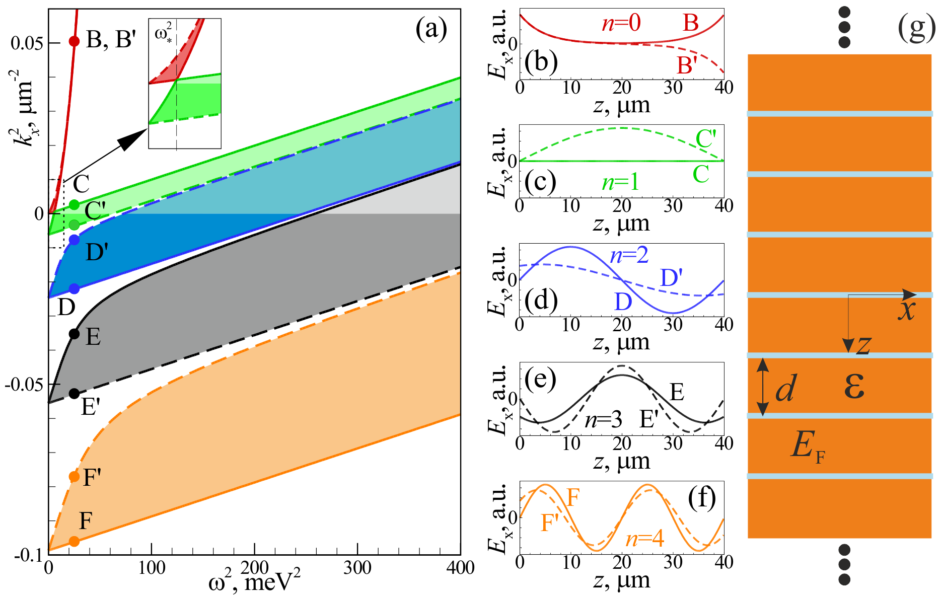
Before considering the dispersion properties in detail, it should be noticed that further in the paper we neglect collisional losses and take the relaxation rate in graphene , i.e., the graphene conductivity is supposed to be purely imaginary. This approximation simplifies the analysis without changing quantitatively the results. The spatial periodicity of the multilayer graphene PC gives rise to the band-gap structure [see Fig.1(a)]: the spectrum is composed of an infinite number of bands [, colored domains in Fig.1(a)], whose boundaries are determined by the Bloch wavevector at the center , or at edge of Brillouin zone [bold solid and bold dashed lines in Fig.1(a), respectively]. One of the bands [, depicted by red color in Fig.1(a)] is polaritonic, where electromagnetic waves are evanescent in direction (with purely imaginary ), and propagating in direction (with purely real ). The other bands () are photonic ones, four of which with are depicted in Fig.1(a) by green, blue, black and orange colors, respectively. All photonic bands are characterized by the propagating nature of the electromagnetic waves in direction (with purely real ), while in -direction they can be either propagating [, shaded by lighter colors in Fig.1(a)], or evanescent [, shaded by darker colors in Fig.1(a)]. The latter are physically meaningful only in confined photonic crystals because they diverge in either plus or minus infinity. Notice that, as follows from the inset in Fig.1(a), the polaritonic and the first photonic band touch each other at a cutoff frequency in the center of the Brillouin zone, (see Appendix A for details). Below this frequency, for , the edge of the polaritonic band at coincides with the light line , while above it, for , the boundary of the polaritonic band detachs from the light line [which coincides with the edge of the first photonic band, solid green line in Fig.1(a)]. At high frequencies, when the localization of the polaritonic modes near each graphene layer is strong, and the SPPs, sustained by neighboring graphene layers, are almost noninteracting. This fact gives rise to the situation when polaritonic dispersion curves for different Bloch wavevectors merge together [see e.g. points B and B’ in Fig.1(a)], although their spatial profiles remain different, as it is evident from Fig.1(b).
Some of the edges of the photonic bands are characterized by an interesting property: at the edges of the photonic bands with odd numbers, () possesses -components of the wavevector
| (23) |
Examples of such modes are C’ and E’ in Figs.1(c) and 1(e). Corresponding expressions for the eigenfunctions (22) can be represented as (details can be found in Appendix A)
| (24) |
When , the edges of the bands with even numbers () possess the same property, i.e.
| (25) | |||
| (26) |
Examples of such modes are D and F in Figs.1(d) and 1(f). It is interesting that expressions for solutions (23), (25) do not contain the graphene conductivity (in other words, their spectrum does not depend upon the graphene’s Fermi energy ): -components and , specified by Eqs.(23) and (25), cancel conductivity-dependent term in the dispersion relation (16). This happens because the derivatives of their spatial profile functions vanish, =0 at [see (24), (26)]. According to (20), it implies zero tangential components of the electric field at graphene layers, clearly seen from the spatial profiles of the modes C’, D, E’, F in Figs.1(c)–1(f). The light line mentioned above is also an eigenmode of the multilayer graphene PC with [see mode C in Fig.1(c)]. It is characterized by absence of the wavevector’s -component and the spatial profile function (further in the paper this mode will be referred to as the light-line mode). The band index for this mode is in the frequency domain (where this mode is the edge of polaritonic band) and above the critical frequency (where this mode is the edge of the first photonic band). As a matter of fact, this mode is a bulk electromagnetic wave propagating in the -direction and with zero longitudinal component of the electric field , i.e. a purely transverse wave.
III Scatttering of polaritonic mode from a single interface between two graphene multilayer PCs
Let us consider now an interface between two graphene multilayer PCs (described in Sec.II). We suppose that both PCs possess the same period , are embedded in the same homogeneous dielectric medium with the dielectric permittivity , and graphene layers are arranged in the same planes along axis . The only difference between these graphene multilayer PCs is the Fermi energy, which is equal to in the first PC (occupying the half-space ) and to in the second one (occupying the half-space ). Further in the text the left and right PCs will be referred to as PC1 and PC2, respectively. Such an interface is schematically depicted in Fig.2.
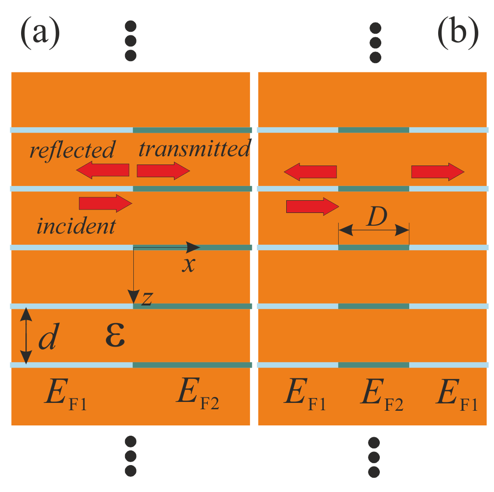
We consider the situation, where the polaritonic mode propagates in the positive direction of the -axis (thus coming from ) and impinges on the aforementioned interface. The main objective of the present section is to describe the scattering of the polaritonic mode on this interface, that is, we want to find the transmission and reflection coefficients of the polaritonic mode as well as to determine which part of its energy is transferred to each of the photonic modes.
In order to do this, we expand the electromagnetic field in series with respect to the graphene multilayer PC eigenmodes (19)–(21). So, the magnetic field and the -component of the electric field in PC1 () can be written as
| (27) | |||
| (28) |
In the same manner, the fields in PC2 can be expressed as
| (29) | |||
| (30) |
In Eqs.(27)–(30) we prescribe the PC index to the spatial profile function , the -component of wavevector , and the amplitude . Also we use band indices and , referring to PC1 and PC2, respectively, and drop the arguments and (which are equal for PC1 and PC2) in functions and amplitudes for brevity. Notice that Eqs.(27) and (28) contain only one mode (polaritonic one with index ) propagating towards the interface in PC1 (referring to the above-mentioned incident wave with amplitude ) and a full set of modes propagating backward from the interface (corresponding to the reflected harmonics with amplitudes ). At the same time, Eqs.(29) and (30) contain only modes propagating in PC2 in the positive direction of -axis, which correspond to the transmitted modes with amplitudes .
The next step is to apply the boundary conditions at the interface [continuity of tangential components of magnetic field , and electric field ] and use the orthogonality of the spatial profile functions,
where the overbar denotes complex conjugation. After applying this orthogonality conditions to Eqs.(27)–(30) we obtain the following equations for the amplitudes:
| (31) | |||
| (32) |
where
| (33) |
It should be noticed that the obtained Eqs.(31) and (32) can also be applied to the case of an interface between the PC and a homogeneous medium (formally in this case ). In this case the spatial profile functions will be as follows:
| (34) | |||
| (35) |
In order to express the reflection and transmission coefficients in terms of energy fluxes, we notice that the component of the Poynting vector along the direction of propagation (-axis) for the -th mode , after substututing the explicit forms of the electromagnetic fields (27)–(30), can be written as
In other words, if the mode is propagating (with purely real ), it carries energy either in positive (sign “+”) or in negative (sign “-”) direction of -axis. In contrast, evanescent modes (with purely imaginary ) do not carry any energy. Thus, we define the coefficients , as the integral characteristics
| (36) | |||
| (37) |
The coefficients , are the reflectance and the transmittance of the polaritonic mode, respectively, while the others () are normalized intensities of higher diffraction orders in PC1 and PC2 (coefficients and , respectively).
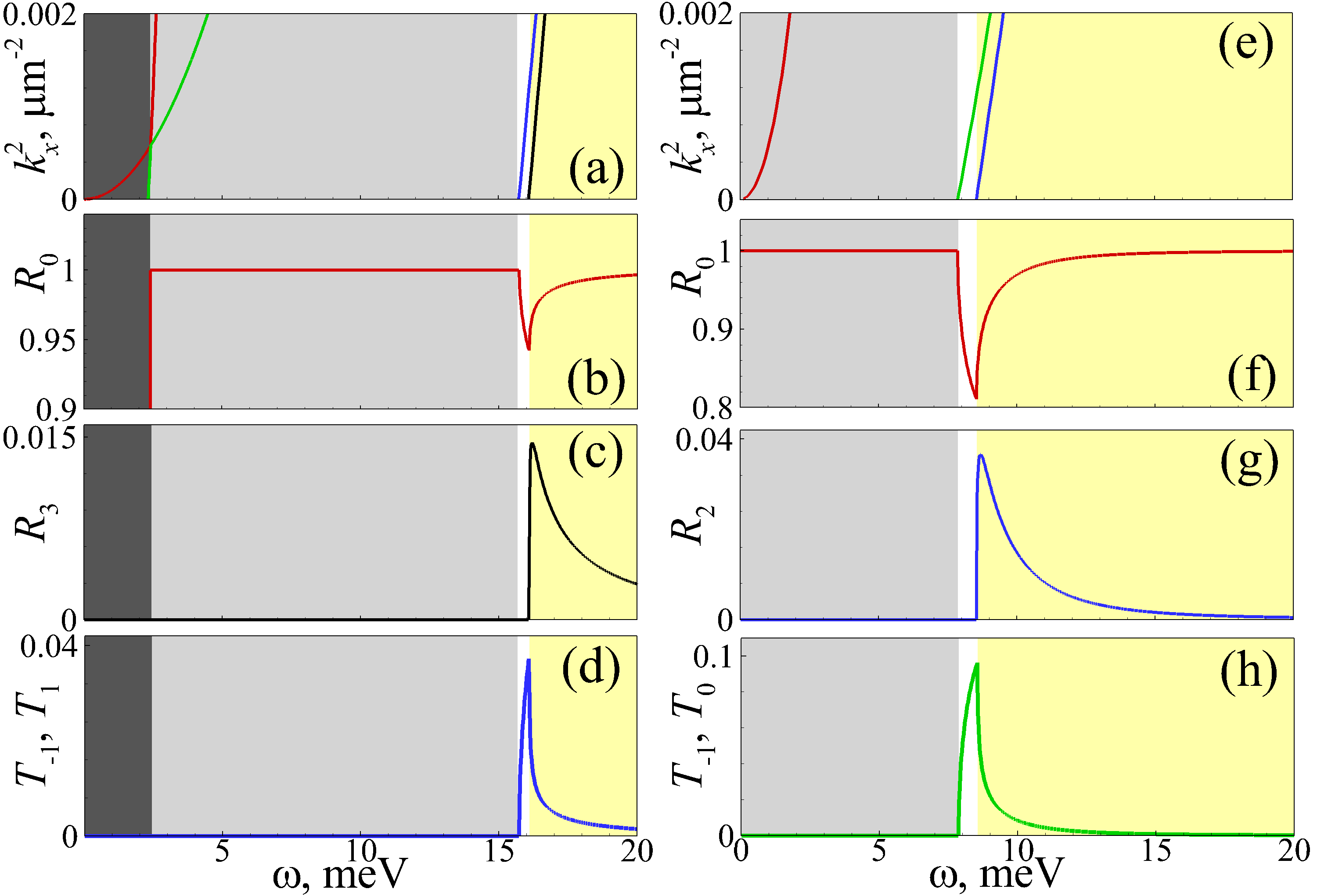
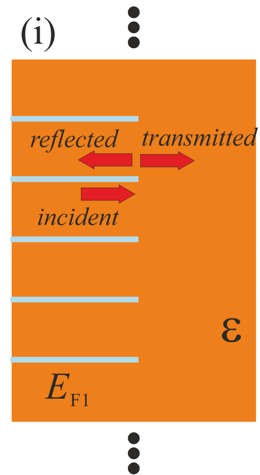
First, we will consider the scattering of an incident polaritonic mode on the interface between the graphene multilayer PC and a homogeneous dielectric, schematically depicted in Fig.3(i). As it was mentioned, in the case [left column in Fig.3] the polaritonic mode exists in the frequency range meV only [light gray, white and yellow domains in Figs.3(a)–3(d)], while the existence of polaritonic mode below the cutoff frequency, is impossible [dark gray domains in in Figs.3(a)–3(d)]. In the frequency range meV [light gray domain in Figs.3(a)–3(d)] there are only two propagating modes in the PC1, namely, polaritonic mode with [depicted by red line in Fig.3(a)] and the light-line mode [depicted by green line in Fig.3(a)]. In the homogeneous dielectric in this frequency range there is only one propagating mode with [see Eq.(34)]. Notice the coincidence of both the shape and dispersion properties of modes with in the homogeneous dielectric and the light-line mode in PC1. Nevertheless, due to the opposite parityNot of the spatial profile functions integral (33), i.e. polaritonic mode can not be coupled to the light-line mode, thus giving rise to the total reflection () of the polaritonic mode in this frequency range, shown in Fig.3(b).
The narrow frequency range [white domain in Figs.3(a)–3(d)] corresponds to the situation when one more mode in PC with [depicted by blue line in Fig.3(a)] as well as two more modes in the homogeneous dielectric, with become propagating. In spite of having the same dispersion properties [compare Eqs.(25) and (35)], these modes possess different spatial profiles [compare Eqs.(26) and (34)]. The incident polaritonic mode , although not being able to couple to the mode in PC due to the opposite parity [see modes B in Fig.1(b) and D in Fig.1(d)], still can couple to the modes in the homogeneous dielectric. The last fact results in the nonzero intensities of these diffraction orders and , shown in Fig.3(d), and a decrease of the polaritonic mode reflectance [Fig.3(b)]. At higher frequencies, meV [yellow domain in Figs.3(a)–3(d)] there is one more propagating mode with in the PC1 with the same parity as the incident polaritonic mode [compare modes B in Fig.1(b) and E in Fig.1(e)], thus allowing their coupling and nonzero intensity of diffraction order [Fig.3(c)]. Nevertheless, the third diffraction order intensity is a decreasing function of frequency. At the same time, the diffraction intensities and the reflectance [see Figs.3(d) and 3(b)] possess a maximum and a minimum, correspondingly, at the boundary of the white and the yellow domains, meV.
The diffraction of the polaritonic mode with [central column in Fig.3] is characterized by the following interesting features. In this case the polaritonic mode can exist at any frequency [red line in Figs.3(e)], thus total reflectance takes place [Fig.3(f)] in the frequency range meV. This frequency range is depicted by light gray shadow in Figs.3(e)–3(h). In the frequency range meV [white domain in Figs.3(e)–3(h)] the energy of the incident mode is partially transformed into that of the propagating modes of the homogeneous dielectric [green line in Fig.3(e)], giving rise to nonzero diffraction orders intensities and [Fig.3(h)]. At the same time, in the frequency range meV [yellow domain in Figs.3(e)–3(h)] the coupling between the polaritonic mode and the photonic mode with becomes possible [Fig.3(g)].
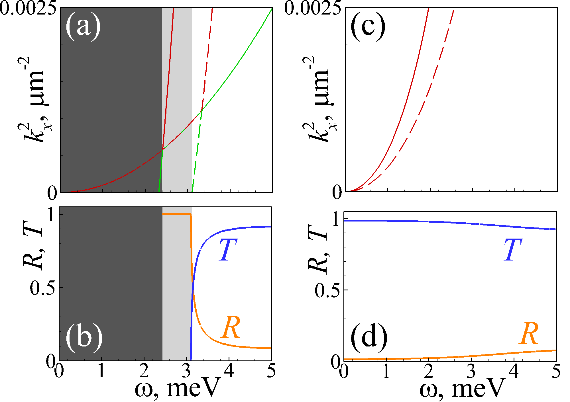
The characteristics of the diffraction of the polaritonic mode at the interface between two graphene multilayer PCs are shown in Fig.4. As in the previous case, polaritonic modes for exist above the cutoff frequencies and in the PC1 and PC2, respectively [nonexistence domain is depicted in Figs.4(a) and 4(b) by dark gray color]. The frequency range meV [light gray domain in Figs.4(a) and 4(b)] is characterized by the existence of polaritonic mode in the PC1, while in the PC2 there is only one propagating mode (the light-line one). Owing to the above-mentioned opposite parity of these modes, mutual coupling between them is not possible, which results in the total reflection [see Fig.4(b)] of the polaritonic mode from the interface between two PCs. In the frequency range meV [white domain in Figs.4(a) and 4(b)] the PC2 contains one more propagating mode, which is photonic () below the cutoff frequency and polaritonic () above it. The last fact gives rise to a gradual decrease of the reflectance and an increase of the transmittance [Fig.4(b)] of the incident polaritonic mode. At the same time, when there is no cutoff frequency for the existence of polaritonic mode [see Fig.4(c)], which results in the nonzero transmittance at any frequency [Fig.4(d)]. It is interesting that for (contrary to the case of ) the reflectance (transmittance) is an increasing (decreasing) function of frequency [compare Figs.4(b) and 4(d)].
IV Scattering of polaritonic mode from the double interface between two graphene multilayer PCs
We now consider the situation [Fig.2(b)] when a graphene multilayer PC of finite width (along the -axis) and with graphene layer’s Fermi energy (further referred to as PC2) is cladded by two semi-infinite PCs which graphene layer are characterized by the Fermi energy (these two PCs will be referred to as PC1 and PC3). As in Sec.II, the incident wave is the polaritonic mode of PC1, propagating in the positive direction of the -axis. Notice, that the only difference between Fig.2(a) and 2(b) is the presence of two interfaces in the last case.
We note that the electromagnetic field in the region can be represented in the same manner as in Eqs.(27) and (28), while inside the region , occupied by the PC2, the field components will have the form:
| (38) | |||
| (39) |
Due to the finite width of the PC2, Eqs.(38) and (39) contain both forward- and backward propagating waves. Finally, in the PC3 (region ) the electromagnetic field components are:
| (40) | |||
| (41) |
Applying the same boundary condition as in Sec.III, we have:
| (42) | |||
| (43) | |||
| (44) | |||
| (45) | |||
For this structure the coefficients are expressed as
while the coefficients are the same as before [Eq.(36)].
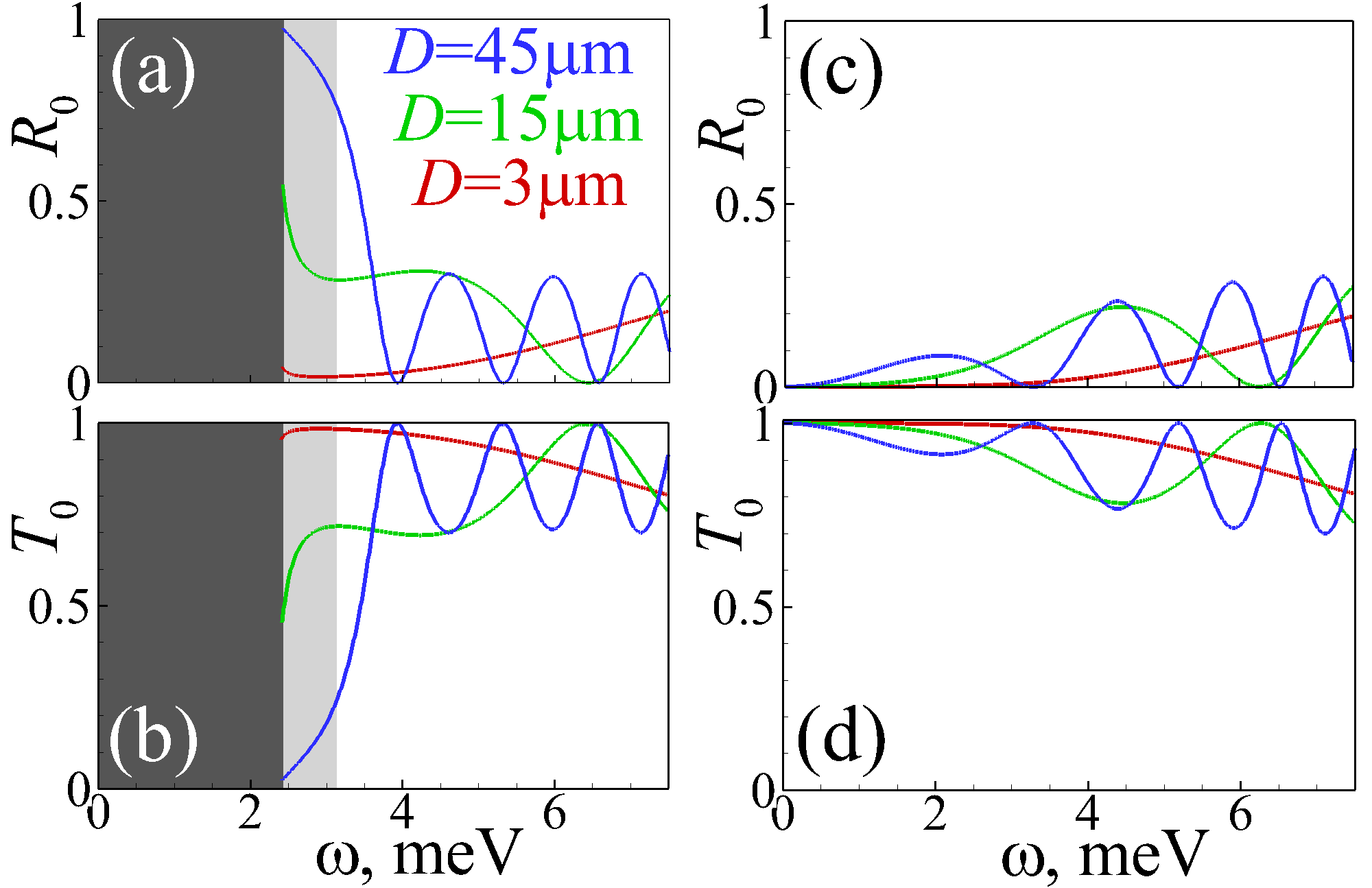
The frequency dependence of the reflectance and transmittance for this structure are shown in Fig.5. For and large width of the PC2 [light gray domain in Figs.5(a) and 5(b)] the reflectance [blue line in Fig.5(a)] of the structure is slightly less than unity in the frequency range meV and it is a decreasing function of the frequency, while the transmittance is nonzero and is an increasing function of (compare with Fig.4(b), where in the case of single interface this range corresponds to the total reflectance , ). The reason for this is the tunneling through the region because there is no propagating mode in PC2. The tunneling rate (and, as a consequence, the transmittance ) gradually grows when the PC2 width, is decreased, compare blue, green and red lines in Fig.5(b). Notice that for small m [red line in Fig.5(b)] almost the whole energy of the incident wave is transmitted via tunneling, thus giving . In the frequency range meV [white domain in Figs.5(a) and 5(b)] one more mode in PC2 becomes propagating, which gives rise to the Fabry-Pérot oscillations of the transmittance and reflectance and the possibility of total transmission (respectively, ). The latter takes place at frequencies, for which the width matches an integer number of polaritonic mode half-wavelengths, that is
| (46) |
The same phenomenon also occurs when [see Figs.5(c) and 5(d)]. The frequencies at which full transmission takes place can be approximated using the Drude model for graphene’s conductivity. Correspondingly, the parameter in the dispersion relation (16) can be approximated by , while we also use the so-called non-retarded approximation for . Under these assumptions the dispersion relation (16) can be rewritten as
which along with Eq.(46) gives
| (47) |
For the case m Eq.(47) gives meV for and meV for , which qualitatively agrees with Figs.5(b) and 5(d) [green line].
The oscillations of the transmittance can be seen as an optical analogue of the well known effect of electron resonant tunneling in a double-barrier heterostructure (DBHS).Chang et al. (1974) The modulation depth of the electromagnetic wave transmission is smaller than in the case of electrons because of the weaker confinement of the former (so that direct tunneling involving only evanescent waves in the PC2 is possible) and also because of the simultaneous presence of several scattering channels.
V Conclusions
We have analysed the scattering of surface plasmon-polaritons generated in a graphene multilayer photonic crystal and propagating across its lateral surface or interface with another graphene multilayer PC with a different band structure (controlled by the graphene’s Fermi energy). In particular, for the low-frequency region where only the polaritonic mode (with imaginary component of the wavevector, ) is propagating in the direction along the graphene sheets (while the modes with real have imaginary , i.e. are evanescent in this sense), we have shown that this mode is totally reflected from the interface between the graphene multilayer PC and a homogeneous dielectric. Nevertheless, in the higher-frequency region where photonic (i.e. propagating with real ) modes are allowed, the partial transformation of the incident polaritonic mode’s energy into that of other diffraction orders (both in PC and in homogeneous dielectric) becomes possible, thus reducing the reflectance of the incident wave. Moreover, by virtue of the reciprocity principle this gives rise to the possibility to excite the PC’s polaritonic eigenmode by an external wave impinging on its edge. In-phase polaritonic mode (with ) can also be totally reflected from the interface between two PCs, while for out-of-phase oscillations (with ) this scenario is impossible. It is also shown that the transmittance and the reflectance of a structure consisting of three photonic crystals and two interfaces between them (we asumed PC1=PC3PC2) exhibit Fabry-Pérot oscillations with a discrete set of frequencies for which total transmission of the polaritonic mode takes place. This effect is similar to the resonant tunneling of electrons in a DBHS where the electric current shows a sharp peak as a function of bias.Chang et al. (1974) Here, in addition to the difference between the Fermi levels of the crystals PC1 and PC2, the electromagnetic wave transmission depends also on the PC wavevector .
Acknowledgments
We acknowledge support from the EC under the Graphene Flagship (Contract No. CNECT-ICT-649953).
Appendix A Approximations for the eigenvalues and eigenfunctions.
Let us consider first the asymptotical behaviour of the polaritonic modes at high frequencies, where the modes with different Bloch wavevector merge. Since SPPs are evanescent waves, it is natural to introduce a decay parameter in -direction, . In this case the dispersion relation (16) can be rewritten as
| (48) |
Notice that in the limiting case the dispersion relation (48) transforms into , i.e. into the dispersion relation for a single graphene sheet. If we consider the situation of being large but finite, the single sheet dispersion relation can be used as zeroth approximation for . This approximation after being sibstituted into the right hand side of Eq.(48), allows for an approximate respresentation of Eq.(48) as
| (49) |
The above-mentioned zeroth approximation for also can be used for approximating the spatial profile function (22), namely:
Even more, since all the phenomena we are interested in take place in the frequency range , we can take into account only the Drude contribution to graphene’s conductivity. Correspondingly, the parameter can be approximated by .
This fact can be used in the approximation of the touching point (cutoff frequency) between the zeroth and first band at , mentioned in Sec.II. Taking into acccount the smallness of in the touch points, one can expand the dispersion relation (16) as
At we have
Taking into account the above-mentioned approximation for we find that (with being purely real) or (with being purely imaginary) in the frequency ranges and , respectively. The last fact well corroborates with the dispersion curve behavior in the vicinity of the cutoff frequency , depicted in Fig.1(a).
From Fig.1(a) it is evident that in the high-frequency region the gaps becomes narrow. We can use this fact in order to approximate the eigenfunctions and the eigenvalues in this region. At the edge of the Brillouin zone () we represent -component of the wavevector in the band with even number () as with being small value () and is determined in Eq.(23). In this case the dispersion relation after the expansion of sine and cosine with respect to can be represented as
from which it is possible to determine
and
In the same manner it is possible to obtain an approximate expression for the spatial profile function (22):
| (50) | |||
with
The same formalism can be applied to the boundaries of the bands with an odd numbers () at the center of Brillouin zone . Thus, we obtain
and
An approximate expression for the spatial profile function (22) can be written
| (51) | |||
with
References
- Maier (2007) S. A. Maier, Plasmonics: Fundamentals and Applications (Springer, New York, 2007).
- Low and Avouris (2014) T. Low and P. Avouris, ACS Nano 8, 1086 (2014).
- Dionne and Atwater (2012) J. A. Dionne and H. A. Atwater, MRS Bulletin 37, 717 (2012).
- Stockman (2011) M. I. Stockman, Phys. Today 64, 39 (2011).
- Khurgin and Boltasseva (2012) J. B. Khurgin and A. Boltasseva, MRS Bulletin 37, 768 (2012).
- de Abajo (2014) F. J. G. de Abajo, ACS Photonics 1 (2014).
- Bludov et al. (2013a) Y. V. Bludov, N. M. R. Peres, and M. I. Vasilevskiy, Journal of Optics 15, 114004 (2013a).
- Stauber (2014) T. Stauber, J. Phys.: Condens. Matter 26, 123201 (2014).
- Chen et al. (2012) J. Chen, M. Badioli, P. Alonso-González, S. Thongrattanasiri, F. Huth, J. Osmond, M. Spasenović, A. Centeno, A. Pesquera, P. Godignon, et al., Nature 487, 77 (2012).
- Fei et al. (2012) Z. Fei, A. S. Rodin, G. O. Andreev, W. Bao, A. S. McLeod, M. Wagner, L. M. Zhang, Z. Zhao, M. Thiemens, G. Dominguez, et al., Nature 487, 82 (2012).
- Gonçalves and Peres (2016) P. A. D. Gonçalves and N. M. R. Peres, An Introduction to Graphene Plasmonics (World Scientific, Singapore, 2016).
- Koppens et al. (2011) F. H. L. Koppens, D. E. Chang, and F. J. G. de Abajo, Nano Lett. 11, 3370 (2011).
- Berman et al. (2010) O. L. Berman, V. S. Boyko, R. Y. Kezerashvili, A. A. Kolesnikov, and Y. E. Lozovik, Physics Letters A 374, 4784 (2010).
- Berman and Kezerashvili (2012) O. L. Berman and R. Y. Kezerashvili, Journal of Physics: Condensed Matter 24, 015305 (2012).
- Arefinia and Asgari (2013) Z. Arefinia and A. Asgari, Physica E: Low-Dimensional Systems and Nanostructures 54, 34 (2013), ISSN 13869477.
- Qin et al. (2014) C. Qin, B. Wang, H. Huang, H. Long, K. Wang, and P. Lu, Optics Express 22, 25324 (2014).
- Chaves et al. (2015) A. J. Chaves, N. M. R. Peres, and F. A. Pinheiro, Phys. Rev. B 92, 195425 (2015).
- Hajian et al. (2013) H. Hajian, A. Soltani-Vala, and M. Kalafi, Optics Communications 292, 149 (2013).
- El-Naggar (2015) S. A. El-Naggar, Optical and Quantum Electronics 47, 1627 (2015).
- Al-sheqefi and Belhadj (2015) F. Al-sheqefi and W. Belhadj, Superlattices and Microstructures 88, 127 (2015).
- Madani and Entezar (2013) A. Madani and S. R. Entezar, Physica B: Condensed Matter 431, 1 (2013).
- Cheng et al. (2015a) Y. H. Cheng, C. Chen, K. Y. Yu, and W. J. Hsueh, Optics Express 23, 28755 (2015a).
- Kaipa et al. (2012) C. S. R. Kaipa, A. B. Yakovlev, G. W. Hanson, Y. R. Padooru, F. Medina, and F. Mesa, Physical Review B - Condensed Matter and Materials Physics 85, 4 (2012).
- Xu et al. (2013) Z. Xu, C. Chen, S. Q. Y. Wu, B. Wang, J. Teng, C. Zhang, and Q. Bao, Graphene-polymer multilayer heterostructure for terahertz metamaterials (2013).
- Sreekanth et al. (2012) K. V. Sreekanth, S. Zeng, J. Shang, K.-T. Yong, and T. Yu, Scientific reports 2, 737 (2012).
- Fan et al. (2013) Y. Fan, Z. Wei, H. Li, H. Chen, and C. M. Soukoulis, Physical Review B 88, 1 (2013), eprint 1311.7037.
- Wang et al. (2012) B. Wang, X. Zhang, F. J. García-Vidal, X. Yuan, and J. Teng, Physical Review Letters 109, 1 (2012).
- Fan et al. (2014) Y. Fan, B. Wang, H. Huang, K. Wang, H. Long, and P. Lu, Optics Letters 39, 6827 (2014).
- Wang et al. (2015a) F. Wang, C. Qin, B. Wang, S. Ke, H. Long, K. Wang, and P. Lu, Optics Express 23, 31136 (2015a).
- Bludov et al. (2015) Y. V. Bludov, D. A. Smirnova, Y. S. Kivshar, N. M. R. Peres, and M. I. Vasilevskiy, Physical Review B 91, 045424 (2015).
- Wang et al. (2015b) Z. Wang, B. Wang, H. Long, K. Wang, and P. Lu, Optics Express 23, 32679 (2015b).
- Sreekanth et al. (2013) K. V. Sreekanth, S. Zeng, K. T. Yong, and T. Yu, Sensors and Actuators, B: Chemical 182, 424 (2013).
- Liu et al. (2014) J.-T. Liu, N.-H. Liu, H. Wang, T.-B. Wang, and X.-J. Li, Physica B: Condensed Matter 452, 66 (2014).
- Sensale-Rodriguez et al. (2012) B. Sensale-Rodriguez, R. Yan, M. M. Kelly, T. Fang, K. Tahy, W. S. Hwang, D. Jena, L. Liu, and H. G. Xing, Nature communications 3, 780 (2012).
- Yan et al. (2012) H. Yan, X. Li, B. Chandra, G. Tulevski, Y. Wu, M. Freitag, W. Zhu, P. Avouris, and F. Xia, Nature Nanotechnology 7, 330 (2012).
- Iorsh et al. (2013) I. V. Iorsh, I. S. Mukhin, I. V. Shadrivov, P. A. Belov, and Y. S. Kivshar, Physical Review B 87, 075416 (2013).
- Zhukovsky et al. (2014) S. V. Zhukovsky, A. Andryieuski, J. E. Sipe, and A. V. Lavrinenko, Physical Review B 90, 155429 (2014).
- Cheng et al. (2015b) M. Cheng, P. Fu, M. Weng, X. Chen, X. Zeng, S. Feng, and R. Chen, Journal of Physics D: Applied Physics 48, 285105 (2015b).
- Vakil and Engheta (2011) A. Vakil and N. Engheta, Science (New York, N.Y.) 332, 1291 (2011).
- Rejaei and Khavasi (2015) B. Rejaei and A. Khavasi, J. of Opt. 17, 075002 (2015).
- Bludov et al. (2013b) Y. V. Bludov, A. Ferreira, N. M. R. Peres, and M. I. Vasilevskiy, International Journal of Modern Physics B 27, 1341001 (2013b).
- (42) Here the parity is considered with respect to the middle of the dielectric slab between the graphene sheets, i.e. the plane .
- Chang et al. (1974) L. L. Chang, L. Esaki, and R. Tsu, Appl. Phys. Lett. 24, 593 (1974).