Electronic and transport properties of the Mn-doped topological insulator Bi2Te3: A first-principles study
Abstract
We present a first-principles study of the electronic, magnetic, and transport properties of the topological insulator Bi2Te3 doped with Mn atoms in substitutional (MnBi) and interstitial van der Waals gap positions (Mni), which act as acceptors and donors, respectively. The effect of native BiTe- and TeBi-antisite defects and their influence on calculated electronic transport properties is also investigated. We have studied four models representing typical cases, namely, (i) Bi2Te3 with and without native defects, (ii) MnBi defects with and without native defects, (iii) the same, but for Mni defects, and (iv) the combined presence of MnBi and Mni. It has been found that lattice relaxations around MnBi defects play an important role for both magnetic and transport properties.
The resistivity is strongly influenced by the amount of carriers, their type, and by the relative positions of the Mn-impurity energy levels and the Fermi energy. Our results suggest strategies to tune bulk resistivities, and also clarify the location of Mn atoms in samples. Calculations indicate that at least two of the considered defects have to be present simultaneously in order to explain the experimental observations, and the role of interstitials may be more important than expected.
pacs:
72.10.Fk, 72.15.Gd, 75.47.Np, 75.50.BbI Introduction
The field of spintronics is connected with a continuous search for new magnetic semiconductors. The most popular in the past were materials based of the group III-V or II-VI semiconductors doped with magnetic elements, mostly with manganese, (Ga,Mn)As being the prototypical case. Dietl and Ohno (2014); Sato et al. (2010) Here, the main idea is to prepare functional compounds where carrier concentrations and magnetic degrees of freedom are entangled.
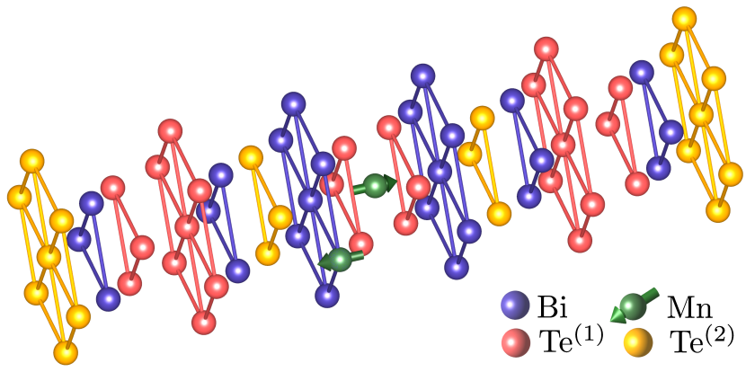
Another class of new materials has tetradymite crystal structure like, e.g., Bi2Te3 or Bi2Se3, known also for their thermoelectric applications. Noh et al. (2008) It should be noted that Bi2Te3 or Bi2Se3 recently attracted a great interest also due to the topological character of their electronic structure which manifests itself in the existence of a Dirac surface state with helical spin texture. Fu et al. (2007); Zhang et al. (2009); Hasan and Kane (2010); Zhang et al. (2010); Hsieh et al. (2009) Their doping by low concentrations of transition metal elements, e.g., by Ti, V, Cr, Mn, or Fe, is a way to add novel functionality to topological insulators.Dietl and Ohno (2014) It has led to ferromagnets with low Curie temperatures below 20 K.Hor et al. (2010); Choi et al. (2005); Lee et al. (2014); Tarasenko et al. (2016) Theoretical calculations,Vergniory et al. (2014) however, obtain a monotonic increase of the Curie temperature with increasing doping. Doping by transition metal impurities leads to formation of carriers, e.g., Mn-impurities in Bi2Te3 which substitute Bi-atoms will act as acceptors. Substitutional Mn positions (MnBi) are assumed in most of the works.Hor et al. (2010); Henk et al. (2012); Choi et al. (2005); Lee et al. (2014) Contrary to this, in experiments many samples have exhibited electron-like conductivity,Lee et al. (2014); Watson et al. (2013); Růžička et al. (2015) which indicates that MnBi cannot be the only defect present. Similarly to (Ga,Mn)As, Mn atoms in Bi2Te3 can also occupy interstitial positions, presumably an octahedral position with 6 nearest Te neighbours in the van der Waals (vdW) gap Watson et al. (2013); Růžička et al. (2015) as shown in Fig. 1. According to first principles calculations Zhang et al. (2013) this position has the lowest formation energy of the three possible interstitial ones and its preference has also been found experimentally.Růžička et al. (2015) In such a case, Mn defects act as donors. Related physical properties like the residual resistivity, magnetoresistance, or anomalous Hall effect, are of great importance for the physical characterization of the doped Bi2Te3 or Bi2Se3.
In addition to the above mentioned intentional doping by transition metal defects there exist also native defects depending on growth conditions, e.g., the Bi-rich or Te-poor samples in Bi2Te3. Such native antisite defects act as acceptors (in Bi-rich conditions) or donors (in Bi-poor conditions), and thus play a key role in controlling bulk transport properties. Both antisite defects are energetically more favourable than possible Te or Bi vacanciesScanlon et al. (2012) in this compound.
Understanding bulk transport is of particular interest regarding the 2D topological surface state contributions to transport measurements. Hor et al. (2011); Hoefer et al. (2014); Brahlek et al. (2015) The aim of the present work is thus a systematic first-principles study of bulk transport properties of Mn-doped Bi2Te3 including the presence of native defects. A prerequisite for such a study is a detailed understanding of corresponding electronic structure properties as manifested, e.g., in modifications of their densities of states (DOS), the type of carriers and the position of impurity levels with respect to the Fermi energy (), which is related to the strength of the impurity scattering. So far, there is no related first-principles study for transport properties of doped topological insulators in the literature, and also the study of alloy electronic structures are very rare. Authors of existing studies limited their attention to the estimate of formation energies of native Scanlon et al. (2012); Oh et al. (2014) and transition metal Zhang et al. (2013) defects using the supercell approach. A combined study of both native and transition metal defects, in particular for low doping concentrations, is technically too difficult in the framework of the supercell approach. A more suitable tool in such cases is the treatment of disorder in the framework of the coherent potential approximation Soven (1967) (CPA), which allows to treat low concentrations of few defect types. The CPA gives reliable concentration trends, but, e.g., the local environment effects are beyond the scope of this method. In this sense, the supercell and CPA methods are complementary. Notably, experiments indicate no clustering of Mn atoms when samples are carefully grown. Tarasenko et al. (2016) Such homogeneous distribution of dopants is an important condition for the CPA applicability. So far there exist two recent theoretical CPA studies Henk et al. (2012); Vergniory et al. (2014) of doped topological insulators including MnBi-doped Bi2Te3, but neglecting possible lattice relaxations. Most importantly, our CPA approach allows a consistent treatment of transport properties using the linear response theory (the Kubo-Greenwood approach). For the first time we provide bulk residual resistivities of Mn-doped Bi2Te3, also with various native defects and both in the basal plane and along the -axis.
II Formalism
The ideal Bi2Te3 consists of quintuple layers, which are separated by vdW gaps. Quintuple layers are composed from hexagonal layers following a Te(I)-Bi-Te(II)-Bi-Te(I) sequence, containing equivalent Bi layers and inequivalent center (Te(II)) and terminating Te(I) layers, see Fig. 1.
The experimental lattice parameters Zhang et al. (2010) are used and we neglect small volume changes due to Mn and antisite dopings. On the other hand, we include possible lattice relaxations around MnBi, but neglect relaxations corresponding to native antisites.
The electronic structure is studied using the Green function version of the tight-binding linear muffin-tin orbital methodSkriver (1984) with atomic-sphere approximation (TB-LMTO-ASA) method, the effect of disorder is included in the CPA. Turek et al. (1997) The local spin-density approximation, the Vosko-Wilk-Nusair exchange-correlation potential Vosko et al. (1980) and the -basis are used. Relativistic corrections were included approximately by adding the on-site spin-orbit coupling term to the scalar-relativistic TB-LMTO Hamiltonian and the value of the spin-orbit coupling was determined self-consistently during calculations. Turek et al. (2008) There are two reasons for the inclusion of the spin-orbit coupling: (i) Te and in particular Bi atoms are heavy elements, and (ii) the bandgap and its value is reproduced reasonably well as compared to the scalar-relativistic case. In the disordered case we have also used a simple screened impurity model Korzhavyi et al. (1995) to improve the treatment of the alloy electrostatics. The empty sphere is used to simulate vdW positions in an ideal Bi2Te3 crystal, which also improves the space filling. The formula unit thus consists of six sublattices. MnBi atoms randomly occupy two equivalent Bi-sublattices in equal amounts, while Mni atoms can occupy randomly part of interstitial positions. Native defects are treated as BiTe and TeBi substitutionals assuming the same concentrations on each of the corresponding sublattices.
The supercell VASP calculations were performed using the projector augmented wave schemeKresse and Joubert (1999) and both the Perdew-Zunger-Ceperly-Alder exchange correlation potential,Perdew and Zunger (1981); Ceperley and Alder (1980) and the generalized gradient approximation Perdew et al. (1996) to simulate Mn defects of both types and to investigate the role of lattice relaxations around Mn atoms. Supercells contained 60 atoms. Mn impurities either substituted one Bi atom, or were placed in the vdW gap position. During finalization of the paper, we became aware of a recent workLi et al. (2014) based on VASP calculations, in which similar electronic structure results for MnBi and Mni were obtained.
Calculations based on the supercell approach indicate that a proper treatment of the size mismatch among Bi- and Mn-atoms for MnBi defects should be considered, it leads to a lattice relaxation around the Mn atom. In the TB-LMTO-CPA calculations we have used an already developed method Kudrnovský and Drchal (1990); Kudrnovský et al. (2009) to include the size mismatch between Bi and Mn atoms treated naturally in the full potential approach Persson and Zunger (2003). In this way the total magnetization and the important features of the DOS, in particular the relative positions of Mn levels with respect to , were reproduced to a good accuracy. We refer the reader to the Supplemental Materialr_S for details. On the other hand, small Mni atoms can be modelled without modifications in the conventional TB-LMTO approach. The supercell calculations obtain negligible lattice relaxations in this case.
As concerns transport properties, we limit ourselves to the diagonal elements of the conductivity tensor to estimate residual resistivities. The formalism for diagonal elements of the conductivity tensor including spin-orbit coupling Turek and Zalezak (2010) has the form identical to that obtained in the scalar-relativistic case. Turek et al. (2002) The present implementation employs a non-random velocity operator formulation Turek et al. (2002), which simplifies the evaluation of disorder-induced vertex corrections. Carva et al. (2006) The estimate of the off-diagonal elements of the conductivity tensor related, e.g., to the anomalous Hall effect, although possible in the present formalism, is beyond the scope of the present study.
We have considered the following models for both the electronic structure and residual resistivities: (i) Model A: Bi2Te3 without and with native acceptors and donors; (ii) Model B: Bi2Te3 with MnBi dopants as well as with native acceptors and donors; (iii) Model C: Bi2Te3 with Mn interstitials (Mni) in the vdW gap position as well as with native acceptors and donors; and (iv) Model D: Combined effect of MnBi and Mni dopants.
III Results and discussion
III.1 Electronic structure
Below we present the DOS’s for studied Models A, B, C, D calculated by the TB-LMTO method. We assume the same concentration of Mn dopants per formula unit in Models B, C, D, i.e., =0.05. Discussion of the DOS’s, namely the amount and the type of carriers and the relative position of Mn-impurity peaks with respect to allows to draw qualitative conclusions about corresponding resistivities shown below in Table 2.
III.1.1 Model A: Bi2Te3 without and with antisite defects
We present in Fig. 2 the total DOS of Bi2Te3 without and with antisite BiTe and TeBi defects. The following conclusions can be done: (i) The ideal Bi2Te3 is an insulator with a narrow gap of 0.11 eV, which compares well with the experimental value of 0.16 eV Harman et al. (1957); Hsieh et al. (2009). The shape of the DOS agrees well with corresponding LMTO bandstructure calculations,Mishra et al. (1997) as well as with calculations based on the full-potential linearized augmented-plane-wave method,Larson et al. (2002) in particular around the gap which is relevant for transport. The band inversion has been obtained similarly to other calculationsZhang et al. (2010); Aguilera et al. (2013). Decomposition of the total DOS into the local Bi- (and Te-) DOS’s reveals a dominating Bi- (Te-) character of the conduction (valence) bands; (ii) BiTe-antisites act as acceptors forming the hole-type conductor while TeBi-antisites act as donors and form the electron-type conductor; and (iii) The disorder in broad -bands is generally weak and the gap survives. One should expect relatively low resistivities controlled in both bands by mobile -orbital type carriers.


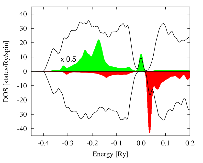
III.1.2 Model B: Bi2Te3 with MnBi defects
The DOS’s for Bi2Te3 with substitutional Mn atoms on Bi-sites without and with Bi/Te co-doping are shown in Fig. 3. We make the following comments: (i) The Mn-doped crystal has halfmetallic character as the gap in the minority states survives (Fig. 3a); (ii) A remarkable feature is the formation of the virtual bound state at in the majority states, while lies in the gap of the minority bands. The resistivity is thus only due to carriers in the narrow Mn impurity band or, equivalently, due to low mobile -electrons and it is thus expected to be large; (iii) Co-doping by BiTe acceptors (Fig. 3b) shifts downwards from the impurity peak deeper into the valence band so that carriers are partly mobile -holes while the majority and minority impurity peaks remain unoccupied. The downward shift of the Mn-minority peak kills the halfmetallic character of the alloy; (iv) Co-doping with TeBi donors (Fig. 3c) acts in the opposite way, namely, is shifted upwards from the majority impurity band into the conduction band, i.e., the conductivity is due to mobile -electrons. The alloy is nearly in a halfmetallic regime due to the minority band gap located just below . In both doping models one thus expects a reduction of the resistivity due to the reduced impurity scatterings and mobile -carriers. Of course, the value of the resistivity in this case also depends on the amount of carriers which is due to corresponding Mn and antisite concentrations; and (v) The neglect of lattice relaxations around MnBi has a dramatic effect on the position of Mn-impurity peaks with respect to .r_S
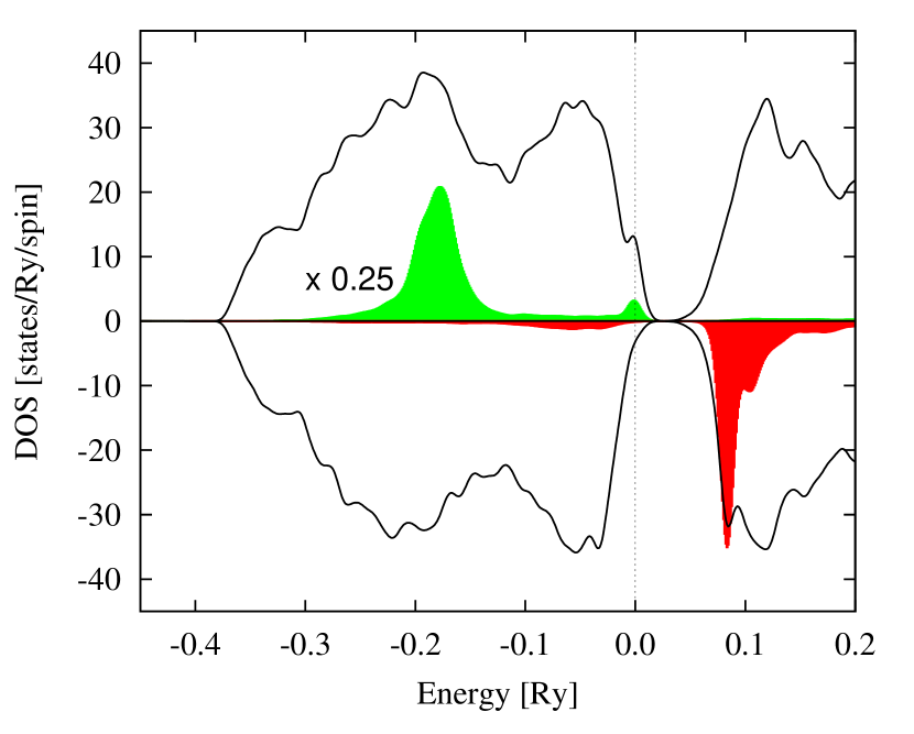
III.1.3 Model C: Bi2Te3 with Mn-interstitials
In Fig. 4 we show the DOS’s for Mni in vdW gap positions without and with native defects. The following conclusions are made: (i) Donors shift into the conduction band. Contrary to the MnBi doping we have now carriers in both majority and minority bands. In this case the conductivity is partly due the mobile -electrons and should be larger than for the Model B (without interstitials). In addition, the minority Mn-peak is quite broad here. Note that the gap in the majority states survives; (ii) Co-doping by BiTe acceptors shifts into the majority gap while it lies partly in the impurity minority band, a situation similar to that in Fig. 3a. In addition, the number of carriers (electrons in Fig. 4a) is reduced by BiTe acceptors which leads to a large sample resistivity; (iii) On the contrary, TeBi atoms donate additional carriers (electrons) into the conduction band, but otherwise the situation is similar to that in Fig. 4a so that one should expect further reduction of resistivity. Interestingly, gaps in both majority and minority bands survive so that alloy is a pure electron-type conductor; and (iv) As mentioned above, there is a negligible effect of lattice relaxations in this case.

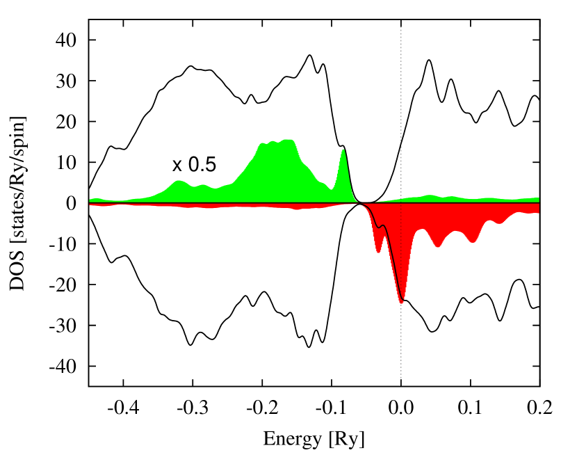
III.1.4 Model D: Bi2Te3 with MnBi defects and Mn interstitials
Finally, we show in Fig. 5 a combined case when both MnBi and Mni defects are present at the same time, while preserving the same nominal Mn concentration as in the previous cases (=0.05). It should be noted that this can be achieved in many ways. Here we show the case when concentrations of Mn-substitutionals and Mn-interstitials are the same, namely, for each of these defects. We make the following comments: (i) The gap in the minority band survives, but lies in the conduction band, while the valence band including the virtual bound state is fully occupied; and (ii) The resistivity for small amounts of Mni donors should be large as will be still partly in Mn -impurity peak (low carrier mobility). The situation will be changed by increasing the amount of Mni at the cost of MnBi-defects. will move away from impurity peak and there will be an increased amount of -orbital carriers in the alloy. In other words, we can interpolate between the above two pure limits, Fig. 3a and Fig. 4a, respectively (see below corresponding resistivities, Fig. 8).

III.1.5 Magnetic moments
We conclude this Section by showing in Table 1 the total magnetic moments per Mn atom and formula unit, and the local magnetic moments on Mn atoms for Models B, C, and D. It should be noted that local moments depend on their definition, in particular on the space included in their calculations. On the other hand the total moments estimated in different methods can be compared reliably. The total moments obtained in VASP calculations (for a slightly smaller Mn concentration =0.042) for models B and C (without interstitials) are 3.97 and 3.73 , respectively, in a good agreement with the presented TB-LMTO values. The co-doping by acceptors/donors in Model B shifts down/up with respect to the undoped case such that it decreases/increases the occupation of majority states, which explains the smaller/larger calculated moments, respectively. The opposite trend is seen for Mn interstitials. In the case of Model D a large occupation of majority states, which include the impurity peak, leads to an increase of the total moment.
| Magnetic moments in Bi2Te3 | |||
|---|---|---|---|
| Models/Types | (a) | (b) + BiTe | (c) + TeBi |
| Model B | 3.99 (3.36) | 2.87 (2.77) | 4.81 (3.72) |
| Model C | 3.57 (3.43) | 4.36 (3.63) | 3.30 (3.38) |
| Model D | 4.40 (3.70/3.56) | ||
| Resistivities in Bi2Te3 | |||
|---|---|---|---|
| Models/Types | (a) | (b) + BiTe | (c) + TeBi |
| Model A | () | 0.13 (0.17) | 0.17 (0.32) |
| Model B | 2.45 (2.88) | 0.49 (0.64) | 0.38 (0.79) |
| Model C | 0.11 (0.23) | 2.95 (3.70) | 0.24 (0.40) |
| Model D | 1.52 (2.46) | ||
III.2 Transport properties of Mn-doped Bi2Te3
Total residual resistivities for the studied Models A, B, C, and D are listed in Table 2 assuming the same total Mn concentration in the formula unit, namely, =0.05. With the knowledge of the above shown DOS’s the results can be qualitatively understood in terms of varying carrier concentrations due to different doping types (acceptors or donors) and relative positions of the Mn impurity level with respect to (low mobility -electron carriers vs high-mobility -electron carriers). We refer the reader to the discussion above (see Section III.1), which of course allows to understand only the relative values of resistivities, not their quantitative values (listed in Table 2).
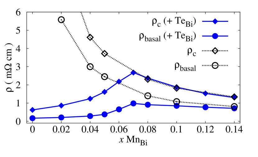
For Models B and C, as well as for Model D, we have also studied corresponding trends with changing Mn concentration. Results are shown in Figs. 6, 7 and 8, respectively. A very different behavior for MnBi substitutionals and Mni interstitials is obtained. The resistivity of MnBi-doped Bi2Te3 decreases monotonically with Mn concentration similarly to the resistivity of Mn-doped GaAs alloys.Turek et al. (2004) The resistivity is affected by the interplay of two factors, namely the increase of strong impurity scattering at virtual bound states in the majority states and the increase of carrier (hole) concentration with a larger Mn doping. The latter effect dominates and the resistivity decreases with Mn doping, exhibiting a non-metallic type of behavior.
Notably the bulk conductivities measured experimentally for Bi2Te3 do not vanish in undoped samples, because of a small amount of inevitable native defects Hor et al. (2011); Hoefer et al. (2014). For this reason one also cannot expect a full agreement between a first principles study assuming only Mn dopants and experiments for low Mn concentration. The presence of native acceptors/donors shifts the Fermi level, can dramatically influence the resistivity (see Table 2) and can be thus used as a tool to control it. We examine MnBi doping in the presence of a fixed amount of TeBi antisites, which leads to a behavior completely different from MnBi doping in the ideal crystal. In this case the doping only increases the amount of scattering, which provides a resistivity increase seen in Fig. 6. This is consistent with the experimentally observed dependencies on Mn doping Hor et al. (2010). For high values of Mn doping (above =0.05 in the studied case) the Fermi level is again in the impurity peak and the situation is comparable to MnBi doping without TeBi antisites. Note that for a wide range of Mn content the antisite presence decreases the resistivity, contrary to the Mn-doped GaAs.Turek et al. (2004); Carva et al. (2007)
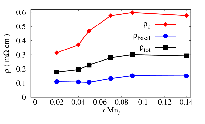
The resistivity of Bi2Te3 doped with Mni behaves differently from that of the MnBi case, see Fig. 7. First, the resistivity due to MnBi doping is much larger as compared to that due to Mni, e.g., about one order of magnitude for =0.05. This difference can be explained by the different character of the conductivity: The MnBi case corresponds to a halfmetal with lying in the narrow virtual bound state and the conductivity is dominated by low mobility -holes. In the case of Mni interstitials both majority and minority channels contribute, and the resistivity is much smaller due to mobile -electrons. When the dopant concentration increases, the carrier concentration increases, but at the same time the impurity scattering at Mn-minority impurity levels increases. The competition of these two effects leads to an increase of the resistivity for smaller Mn concentrations, but for higher ones there is a saturation and one can even observe a small decrease at large Mn doping. On the other hand, absolute values of the resistivity remain much smaller as compared to that due to MnBi atoms. A comparison with experiments is rather difficult, as reported values vary for bulk samples and those prepared by molecular beam epitaxy. Also, it is not clear what is the nature of native defects and sometimes even the carrier type is changed during doping. We have found in literature values ranging from 0.6 mcm Lee et al. (2014) to 1.25 mcm Hor et al. (2010) or even to 2.5mcm.Choi et al. (2005) Calculated values fall in this experimental range of resistivities. A more detailed comparison is difficult due to insufficient details concerning types of defects, their types and amounts in the sample.
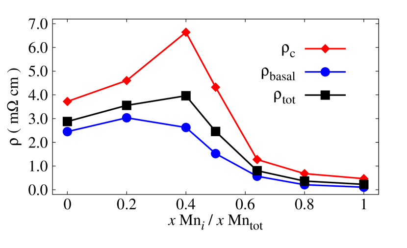
An alternative way is to vary the ratio between MnBi and Mni dopants present together in the sample. It should be noted that such ratios are not easy to control intentionally as it is dictated by the thermodynamics of the sample preparation and its annealing. On the other hand, it is interesting theoretically to consider this effect in some detail. This is shown in Fig. 8, where we present calculated resistivities for a fixed total Mn concentration =0.05 as a function of the ratio of concentrations of Mni () and Mn-substitutional () atoms. We can thus interpolate between Model B and Model C. An increased amount of donor-type Mn interstitials leads first to the increase of the total resistivity due to the reduced carrier concentration (MnBi acceptor concentration is reduced by donors), but a further increase of donors shifts from the MnBi virtual bound state to the conduction band and both majority and minority channels now contribute to the current, thus reducing the resistivity until we have a low resistivity electron-like case with a high content of Mni (see Fig. 4a and Table 2). Note that the values of the resistivity vary by one order of magnitude and reach the value of 1.25 mcm found experimentally.Hor et al. (2010)
In Figs. 6-8 we also show the decomposition of the total resistivity into contributions along the - and in the basal plane indicating a large value of the structural resistivity anisotropy. Notably the resistivity is always higher for the direction along the -axis, which is probably due to the smaller wavefunction overlap across the vdW gap.
Wei et al. Wei et al. (2015) have measured samples of Mn-doped Bi2Se3 with both electron and hole carriers, and obtained an order of magnitude higher resistivity for hole-type conductor than for the electron-type one. Although the exact nature of defects is not known there, this finding is in a qualitative agreement with our calculations for Bi2Te3, where defects providing extra electrons lead to an overall lower resistivity.
IV Conclusions
We have demonstrated the ability of the TB-LMTO-CPA method to capture essential features of the electronic structure of Bi2Te3 doped with Mn atoms. An ideal Bi2Te3 is an insulator with a gap only slightly underestimated in comparison with the experiment. We have reproduced the calculated magnetic moments and general DOS features for MnBi acceptors and Mni donors employing analogous full-potential supercell VASP calculations. In particular, the MnBi virtual bound state with Fermi energy lying in the impurity peak is obtained in both methods, although in TB-LMTO-CPA calculations the effect of the large mismatch of sizes of Bi- and Mn-atoms was included approximately. This justifies the use of the TB-LMTO-CPA to estimate the electronic structure and for the first time transport properties also for more complex, but realistic cases: systems in which native antisite impurities (BiTe donors and TeBi acceptors) are present in addition to Mn atoms.
Antisite doping allows to control the number and the type of carriers present in the sample and thus its resistivity. This was documented by studying four different models, namely, Bi2Te3 with/without native defects and MnBi and Mni with/without native defects. We have also considered alloys containing both types of Mn-dopants. Detailed analysis of the DOS for the studied models allows to understand relative values of corresponding resistivities depending on the character of their carriers, namely, low mobility -electrons in impurity bands and high mobility -holes/electrons in valence/conduction bands. In general, low conductivities for MnBi doping is due to the low mobility of dominating -holes while much higher conductivity of Mni is due to dominating -electron transport. Partial addition of Mni into MnBi-doped system leads to further decrease of conductivity as long as the Fermi level remains in the impurity peak. Overall the variation of the amount of native defects and/or partly also the amount of MnBi and Mni in the sample allows to tune the value of the conductivity within a wide range of values. Another important feature is the high structural anisotropy of the conductivity tensor, with its components in the basal plane always higher than the one along the -axis.
Acknowledgements.
This work was supported by the Czech Science Foundation Grant no. 14-30062S. JH acknowledges the Purkyně fellowship program of the Czech Academy of Sciences.References
- Dietl and Ohno (2014) T. Dietl and H. Ohno, Rev. Mod. Phys. 86, 187 (2014).
- Sato et al. (2010) K. Sato, L. Bergqvist, J. Kudrnovský, P. H. Dederichs, O. Eriksson, I. Turek, B. Sanyal, G. Bouzerar, H. Katayama-Yoshida, V. A. Dinh, et al., Rev. Mod. Phys. 82, 1633 (2010).
- Noh et al. (2008) H.-J. Noh, H. Koh, S.-J. Oh, J.-H. Park, H.-D. Kim, J. D. Rameau, T. Valla, T. E. Kidd, P. D. Johnson, Y. Hu, et al., EPL (Europhysics Letters) 81, 57006 (2008).
- Fu et al. (2007) L. Fu, C. L. Kane, and E. J. Mele, Phys. Rev. Lett. 98, 106803 (2007).
- Zhang et al. (2009) H. Zhang, C.-X. Liu, X.-L. Qi, X. Dai, Z. Fang, and S.-C. Zhang, Nat Phys 5, 438 (2009).
- Hasan and Kane (2010) M. Z. Hasan and C. L. Kane, Rev. Mod. Phys. 82, 3045 (2010).
- Zhang et al. (2010) W. Zhang, R. Yu, H.-J. Zhang, X. Dai, and Z. Fang, New Journal of Physics 12, 065013 (2010).
- Hsieh et al. (2009) D. Hsieh, Y. Xia, D. Qian, L. Wray, F. Meier, J. H. Dil, J. Osterwalder, L. Patthey, A. V. Fedorov, H. Lin, et al., Phys. Rev. Lett. 103, 146401 (2009).
- Hor et al. (2010) Y. S. Hor, P. Roushan, H. Beidenkopf, J. Seo, D. Qu, J. G. Checkelsky, L. A. Wray, D. Hsieh, Y. Xia, S.-Y. Xu, et al., Phys. Rev. B 81, 195203 (2010).
- Choi et al. (2005) J. Choi, H.-W. Lee, B.-S. Kim, S. Choi, J. Choi, J. H. Song, and S. Cho, Journal of Applied Physics 97, 10D324 (2005).
- Lee et al. (2014) J. S. Lee, A. Richardella, D. W. Rench, R. D. Fraleigh, T. C. Flanagan, J. A. Borchers, J. Tao, and N. Samarth, Phys. Rev. B 89, 174425 (2014).
- Tarasenko et al. (2016) R. Tarasenko, M. Vališka, M. Vondráček, K. Horáková, V. Tkáč, K. Carva, P. Baláž, V. Holý, G. Springholz, V. Sechovský, et al., Physica B: Condensed Matter 481, 262 (2016).
- Vergniory et al. (2014) M. G. Vergniory, M. M. Otrokov, D. Thonig, M. Hoffmann, I. V. Maznichenko, M. Geilhufe, X. Zubizarreta, S. Ostanin, A. Marmodoro, J. Henk, et al., Phys. Rev. B 89, 165202 (2014).
- Henk et al. (2012) J. Henk, M. Flieger, I. V. Maznichenko, I. Mertig, A. Ernst, S. V. Eremeev, and E. V. Chulkov, Phys. Rev. Lett. 109, 076801 (2012).
- Watson et al. (2013) M. D. Watson, L. J. Collins-McIntyre, L. R. Shelford, A. Coldea, D. Prabhakaran, S. C. Speller, T. Mousavi, C. Grovenor, Z. Salman, S. R. Giblin, et al., New Journal of Physics 15, 103016 (2013).
- Růžička et al. (2015) J. Růžička, O. Caha, V. Holý, H. Steiner, V. Volobuiev, A. Ney, G. Bauer, T. Duchoň, K. Veltruská, I. Khalakhan, et al., New Journal of Physics 17, 013028 (2015).
- Zhang et al. (2013) J.-M. Zhang, W. Ming, Z. Huang, G.-B. Liu, X. Kou, Y. Fan, K. L. Wang, and Y. Yao, Phys. Rev. B 88, 235131 (2013).
- Scanlon et al. (2012) D. O. Scanlon, P. D. C. King, R. P. Singh, A. de la Torre, S. M. Walker, G. Balakrishnan, F. Baumberger, and C. R. A. Catlow, Advanced Materials 24, 2154 (2012).
- Hor et al. (2011) Y. Hor, J. Checkelsky, D. Qu, N. Ong, and R. Cava, Journal of Physics and Chemistry of Solids 72, 572 (2011).
- Hoefer et al. (2014) K. Hoefer, C. Becker, D. Rata, J. Swanson, P. Thalmeier, and L. H. Tjeng, Proceedings of the National Academy of Sciences 111, 14979 (2014).
- Brahlek et al. (2015) M. Brahlek, N. Koirala, N. Bansal, and S. Oh, Solid State Communications 215-216, 54 (2015).
- Oh et al. (2014) M. W. Oh, J. H. Son, B. S. Kim, S. D. Park, B. K. Min, and H. W. Lee, Journal of Applied Physics 115, 133706 (2014).
- Soven (1967) P. Soven, Phys. Rev. 156, 809 (1967).
- Skriver (1984) H. Skriver, The LMTO Method: Muffin-Tin Orbitals and Electronic Structure (Springer-Verlag, Berlin, 1984).
- Turek et al. (1997) I. Turek, V. Drchal, J. Kudrnovský, M. Šob, and P. Weinberger, Electronic Structure of Disordered Alloys, Surfaces and Interfaces (Kluwer, Boston, 1997).
- Vosko et al. (1980) S. H. Vosko, L. Wilk, and M. Nusair, Can. J. Phys. 58, 1200 (1980).
- Turek et al. (2008) I. Turek, V. Drchal, and J. Kudrnovský, Philosophical Magazine 88, 2787 (2008).
- Korzhavyi et al. (1995) P. A. Korzhavyi, A. V. Ruban, I. A. Abrikosov, and H. L. Skriver, Phys. Rev. B 51, 5773 (1995).
- Kresse and Joubert (1999) G. Kresse and D. Joubert, Phys. Rev. B 59, 1758 (1999).
- Perdew and Zunger (1981) J. P. Perdew and A. Zunger, Phys. Rev. B 23, 5048 (1981).
- Ceperley and Alder (1980) D. M. Ceperley and B. J. Alder, Phys. Rev. Lett. 45, 566 (1980).
- Perdew et al. (1996) J. P. Perdew, K. Burke, and M. Ernzerhof, Phys. Rev. Lett. 77, 3865 (1996).
- Li et al. (2014) Y. Li, X. Zou, J. Li, and G. Zhou, The Journal of Chemical Physics 140, 124704 (2014).
- Kudrnovský and Drchal (1990) J. Kudrnovský and V. Drchal, Phys. Rev. B 41, 7515 (1990).
- Kudrnovský et al. (2009) J. Kudrnovský, F. Máca, I. Turek, and J. Redinger, Phys. Rev. B 80, 064405 (2009).
- Persson and Zunger (2003) C. Persson and A. Zunger, Phys. Rev. B 68, 035212 (2003).
- (37) See Supplemental Material at [URL will be inserted by publisher] for details of the treatment of alloy disorder with unequal constituent atom radii.
- Turek and Zalezak (2010) I. Turek and T. Zalezak, Journal of Physics: Conference Series 200, 052029 (2010).
- Turek et al. (2002) I. Turek, J. Kudrnovský, V. Drchal, L. Szunyogh, and P. Weinberger, Phys. Rev. B 65, 125101 (2002).
- Carva et al. (2006) K. Carva, I. Turek, J. Kudrnovský, and O. Bengone, Phys. Rev. B 73, 144421 (2006).
- Harman et al. (1957) T. Harman, B. Paris, S. Miller, and H. Goering, Journal of Physics and Chemistry of Solids 2, 181 (1957).
- Mishra et al. (1997) S. K. Mishra, S. Satpathy, and O. Jepsen, Journal of Physics: Condensed Matter 9, 461 (1997).
- Larson et al. (2002) P. Larson, V. A. Greanya, W. C. Tonjes, R. Liu, S. D. Mahanti, and C. G. Olson, Phys. Rev. B 65, 085108 (2002).
- Aguilera et al. (2013) I. Aguilera, C. Friedrich, G. Bihlmayer, and S. Blügel, Phys. Rev. B 88, 045206 (2013).
- Turek et al. (2004) I. Turek, J. Kudrnovský, V. Drchal, and P. Weinberger, J. Phys.: Condens. Matter 16, S5607 (2004).
- Carva et al. (2007) K. Carva, I. Turek, and J. Kudrnovský, J. Magn. Magn. Mater. 310, 2123 (2007).
- Wei et al. (2015) Z. Wei, L. Lv, M. Zhang, X. Yang, and Y. Zhao, Journal of Superconductivity and Novel Magnetism 28, 2083 (2015).
Supplemental material
TREATMENT OF ALLOY DISORDER
There are few relevant problems to be addressed when studying physical properties of present random systems, namely: (i) a reliable reproduction of the concentrations trends, (ii) a consistent treatment of the transport relaxation times or related spectral properties of alloys, (iii) the effect of lattice relaxations and local environment effects, in particular in systems with large size mismatch of alloy components, and (iv) the possibility to treat few different impurities in the system. There exist two methods which address above problems using different tools: the supercell (SC) approach, specifically that using the pseudo-potential approach (e.g., like the VASP vasp ), and the coherent potential approximation (CPA). lmto_cpa ; book Both methods fulfil well the property (i), as well as the property (iv), although the CPA is technically more handy in this case. The property (ii) is addressed naturally in the framework of the considered methods only by the CPA, while the SC approach requires additional external tools. On the other hand, the SC method excels in the property (iii) relevant in the present case of the large atom-size mismatch where lattice relaxations/local environment effects can be important.
We will first address the problem of lattice relaxations and their relevance for MnBi and Mni defects in Bi2Te3 using the SC-VASP approach. In the next step we will indicate how the effect of lattice relaxations can be included approximately in the TB-LMTO-CPA approach which is then used for transport studies. As a result, we have found that a combination of both methods, each of which represents an alternative approach to the disordered alloy, is a useful tool for the study of transport properties of complex alloys.
IV.1 Effect of lattice relaxations: SC-VASP approach
The electronic structure of MnBi and Mni is studied using the Bi23MnBiTe36 (60 atoms) and Bi24MniTe36 (61 atoms) supercells, respectively. This corresponds to the nominal Mn-doping of 4.2% (1/24). The van der Waals gap interstitial position was assumed for Mni. The projector augmented wave method as implemented in the VASP codes vasp was used. We have tested both the LDA zca and the GGA pbe approaches but results are very similar. Therefore we show below the results for the LDA case in order to compare with the modified TB-LMTO-CPA method. The Brillouin zone was sampled by 10102 k-vectors, the plane wave cutoff energy was 400 eV, the total energy error was better than 0.05 meV per supercell, and the structure was optimized until forces acting on each atom were smaller than 2.5 meV/Å. During the total energy minimization we have neglected volume changes due to the doping and fixed volume to that corresponding to the ideal Bi2Te3. All calculations were scalar-relativistic ones and when calculating the densities of states (DOS) the Gaussian broadening of 0.1 eV was used. The distances between Mn and the first and the second nearest Te atom were relaxed from 3.03 Å to 2.82 Å, and from 3.25 Å to 2.90 Å, respectively.
The total and Mn-resolved densities of states (DOS) are shown for the relaxed (Fig. S1) and unrelaxed (Fig. S2) MnBi, respectively, as well as for Mni (Fig. S3). The most important conclusion is the relevance of lattice relaxations for MnBi defects. We observe a clearly pronounced virtual bound state at the Fermi energy EF for majority states, at the top of the valence band. This state has a pronounced effect on transport properties, which depend sensitively on the electronic structure at EF. The corresponding minority state is lying in the unoccupied conduction band close to its edge. Very similar results but assuming the GGA rather than LDA and including the spin-orbit coupling were obtained recently in Ref. cinane, .
The model without lattice relaxations differs significantly due to the shift of majority/minority Mn-states downward/upward in energy, which results in a much smaller impurity scattering at EF and thus leads to a reduced resistivity. The local Mn-DOS for the unrelaxed case is very similar to that obtained in Ref. henk, for a closely related case of MnSb in Sb2Te3. On the other hand, negligible lattice relaxations were found for Mni because a small Mn-atom easily accommodates in large empty van der Waals site, contrary to the substitutional MnBi case with the large size mismatch between Mn and Bi.
IV.2 Effect of lattice relaxations: TB-LMTO-CPA
Methods using the spherical approximation for potentials like, e.g., the present TB-LMTO-CPA approach, cannot determine reliably forces and thus lattice/layer relaxations. On the other hand, knowing them from the experiment or full potential calculations, it is possible to include their effect on the electronic structure approximately. For example, the effect of layer relaxations for fcc-Fe/Ir(001) overlayer was included approximately in Ref. feir, and results were in a good agreement with full potential calculations, in particular the antiferromagnetic ground state was obtained correctly only if layer relaxations are included. It should be emphasized that the method sketched below is not a substitute for full potential methods but rather a tool how to capture main effects of lattice relaxations approximately and exploit them for the study of complex related physical properties, like e.g. the transport in the present case.
The LMTO theory depends on two types of Wigner-Seitz radii, namely , which defines the volume of the alloy, and the local radius corresponding to atomic species (=A,B) in an alloy A1-xBx. skriver ; lmto_cpa The conventional choice is = for all atoms. We have modified this choice locally for =Mn,Bi in such a way that the volume of the Bi-sublattice, , is preserved. According to the transformation properties of the LMTO structure constants skriver ; lmto_cpa this leads to a corresponding modification of hopping integrals, and during the selfconsistent loop also to the change of potential parameters. It should be noted that in the past we have tested this approach also for the zincblende GaAs doped with a low concentration of small nitrogen atoms substituting As-sites, a situation similar to that of MnBi, but for a non-magnetic impurity. Using this approach, we have correctly reproduced, in agreement with the full potential study zunger , the downward shift of the nitrogen level for the case with lattice relaxations included as compared to the unrelaxed case.
We have chosen specifically, =2.8 a.u., typical native value for solid state Mn, and accordingly. It should be noted, that radii are used for the solution of the LDA Schrödinger equation. book Corresponding DOS’s (see Fig. 3a and Fig. 4a in the main text) demonstrate that the main features obtained in the SC-VASP calculations (see Fig. S1 and Fig. S3 in this Supplement) were reasonably well reproduced. Small differences can be ascribed to the fact that the finite Gaussian broadening inside the Brillouin zone was used for SC-VASP, as contrasted to the anisotropic damping due to the CPA. No modifications were done for the case of BiTe and TeBi antisites.
References
- (1) G. Kresse and D. Joubert, Phys. Rev. B 59, 1758 (1999).
- (2) J. Kudrnovský and V. Drchal, Phys. Rev. B 41, 7515 (1990).
- (3) I. Turek, V. Drchal, J. Kudrnovský, M. Šob, and P. Weinberger, Electronic Structure of Disordered Alloys, Surfaces and Interfaces (Kluwer, Boston, 1997).
- (4) J. P. Perdew and A. Zunger, Phys. Rev. B 23, 5048 (1981); D. M. Ceperley and B. J. Alder, Phys. Rev. Lett. 45, 566 (1980).
- (5) J.P. Perdew, K. Burke, and M. Ernzerhof, Phys. Rev. Lett. 77, 3865 (1996).
- (6) Y. Li, X. Zou, J. Li, and G. Zhou, J. Chem. Phys. 140, 124704 (2014).
- (7) M.G. Vergniory, M.M. Otrokov, D. Thonig, M. Hoffmann, I.V. Maznichenko, M. Geilhufe, X. Zubizarreta, S. Ostanin, A. Marmodoro, J. Henk, et al., Phys. Rev. B 89, 165202 (2014).
- (8) J. Kudrnovský, F. Máca, I. Turek, and J. Redinger, Phys. Rev. B 80, 064405 (2009).
- (9) H. Skriver, The LMTO Method: Muffin-Tin Orbitals and Electronic Structure, (Springer-Verlag, 1984, Berlin).
- (10) C. Persson and A. Zunger, Phys. Rev. B 68, 035212 (2003).