The two gap transitions in Ge1-xSnx: effect of non-substitutional complex defects
Abstract
The existence of non-substitutional -Sn defects in Ge1-xSnx was confirmed by emission channeling experiments [Decoster et al., Phys. Rev. B 81, 155204 (2010)], which established that although most Sn enters substitutionally (-Sn) in the Ge lattice, a second significant fraction corresponds to the Sn-vacancy defect complex in the split-vacancy configuration ( -Sn ), in agreement with our previous theoretical study [Ventura et al., Phys. Rev. B 79, 155202 (2009)]. Here, we present our electronic structure calculation for Ge1-xSnx, including substitutional -Sn as well as non-substitutional -Sn defects. To include the presence of non-substitutional complex defects in the electronic structure calculation for this multi-orbital alloy problem, we extended the approach for the purely substitutional alloy by Jenkins and Dow [Jenkins and Dow, Phys. Rev. B 36, 7994 (1987)]. We employed an effective substitutional two-site cluster equivalent to the real non-substitutional -Sn defect, which was determined by a Green’s functions calculation. We then calculated the electronic structure of the effective alloy purely in terms of substitutional defects, embedding the effective substitutional clusters in the lattice. Our results describe the two transitions of the fundamental gap of Ge1-xSnx as a function of the total Sn-concentration: namely from an indirect to a direct gap, first, and the metallization transition at higher . They also highlight the role of -Sn in the reduction of the concentration range which corresponds to the direct-gap phase of this alloy, of interest for optoelectronics applications.
pacs:
71.20.Nr,71.55.Ak,71.15.-mI Introduction
The semiconductor technology based on Si has limitations for optoelectronic and photovoltaic device applications, related to the indirect nature of the fundamental bandgap which results in inefficient absorption and emission of light. To overcome these limitations, direct energy-gap materials based on group IV semiconductors have been searched.Hull-1999 ; Menendez-2002 ; Menendez-2006 ; Goodman-1982 Among group-IV elements, Ge is considered an important candidate to replace Si in semiconducting applications.Menendez-2002 Compared to Si, Ge has a larger free-carrier mobility and a lower dopant activation temperature,Hull-1999 which makes it an attractive material in future metal-oxide semiconductor field-effect transistors.Yeo-2005 ; Yang-2007
Ge1-xSnx also attracted considerable attention because it becomes a direct bandgap semiconductor above 6-10% Sn without external mechanical strain. The tunability of its gap with composition makes Ge1-xSnx a highly interesting material for infrared applications, especially at low Sn concentrations ()Atwater . Theoretical calculations indicated that strained Ge1-xSnx () would exhibit enhanced electron and hole mobility, which could make the alloy also interesting for high-speed integrated circuits.Sau-2007 ; liu-APE2015 The integration of Ge in Si-based photonics is important for advances in the performance of detectors, modulators, and emitters. Recently there have been reports of room temperature direct bandgap emission for Si-substrate-based Ge p-i-n heterojunction photodiode structures, operated under forward bias.kasper2011 A temperature-dependent photoluminescence (PL) study has been conductedDu2014 in Ge1-xSnx films with Sn compositions of 0.9, 3.2, and 6.0 grown on Si. The competition between the direct and indirect bandgap transitions was clearly observed. The relative peak intensity of the direct transition with respect to the indirect transition increases with an increase in temperature, indicating the direct transition dominates the PL at high temperatures. Furthermore, as Sn composition increases, a progressive enhancement of the PL intensity corresponding to the direct transition was observed,Du2014 due to the reduction of the direct-indirect valley separation, which experimentally confirms that Ge1-xSnx grown on Si becomes a group IV-based direct bandgap material by increasing the Sn content. More recently, the fabrication and properties of Ge1-xSnx () diodes (LEDs) were reported.menendez2015 Electroluminiscence results indicated that emission properties depend very sensitively on the Sn-concentrations on both sides of the junctions, making this system not only a serious candidate for laser devices but also an ideal model system to study the properties of quasi-direct light emitting devices.
Experimental studies in group-IV alloys were hindered for a long time by sample preparation problems. When Ge1-xSnx samples are experimentally prepared, the distribution of the Sn atoms in the Ge matrix depends on the growth conditions: Sn-atoms can enter randomly, form a regular superstructure, or coalesce into a larger cluster. Below 13∘C, pure Sn exists in the -Sn (gray tin) phase with diamond structure, but it undergoes a phase transition to -Sn (white-tin) above this temperature.cardona1985 Experiments have shown that a problem with the incorporation of Sn into the Ge lattice is the large 17 lattice mismatch between these elements, and the instability of the diamond-cubic structure of -Sn above 13∘C.Menendez-2006 ; Gurdal Although Ge1-xSnx alloys have been successfully grown by molecular beam epitaxy Lin-TSF2012 , chemical vapor deposition Menendez-2006 , and enhanced direct bandgap luminescence has been demonstrated for up to 8% Sn Chen2011 ; Menendez2012 , at higher Sn-concentrations several limitations arise due to the low thermodynamic solid solubility of Sn in the Ge crystal, which is less than 1 and in many cases the material quality is questionable due to the propensity of Sn to segregate toward the film surface.Menendez-2006 ; Gurdal ; Wegscheider Recently, the fabrication of high quality Ge1-xSnx on InGaAs buffer layers using low-temperature growth by molecular beam epitaxy was reported.Lin-TSF2012 X-ray difraction, secondary ion mass spectroscopy and transmission electron microscopy studies, demostrated that up to 10.5 Sn had been incorporated into Ge1-xSnx thin films without Sn precipitation.Lin-TSF2012 More recently, for Ge1-xSnx homogeneous epitaxial layers were grown on InP substrates for the range .Nakatsuka2013 the direct bandgap for the range was obtained through photon absorption spectra measured with Fourier transform infrared spectroscopy.
Experimentally, a series of values have been reported for the critical Sn concentration for the indirect to direct gap transition, hereafter denoted : starting from Atwater et al. Atwater whose optical absorption experiments predicted , followed by Ladrón de Guevara et al.Ladron2007 who reported from transmittance measurements, D’Costa et al.Menendez-2006 reported with ellipsometry experiments, and more recently Chen et al.Chen2011 reported using photoluminescence. Then, was suggested, based on photoluminescence studies of strain free-GeSn layers Chen2011 ; Menendez2012 . In 2013 Ryu et al.Ryu2013 , by means of temperature-dependent photoluminescence experiments of Ge/Si and Ge1-ySny/Si, indicated a possible indirect-to-direct bandgap transition at Sn content , consistent with DFT calculations in Ref. Ying2008, . More recently, by a fit to experimental data in Ge1-xSnx using a theoretical model of the bandgap bowing, Gallagher et al.gallagher2014 estimated a crossover concentration of , significantly increased from earlier estimations based on a strictly quadratic compositional dependence of the bandgaps in Ref.jiang2014, , who obtained .
The incorporation of Sn in the Ge matrix has been investigated theoretically by Ventura et al.CFB-2009 ; CFB-Physica Through local defect electronic calculations, the formation of several complex Sn-defects in Ge1-xSnx alloy was analyzed: confirming that at low Sn concentrations substitutional -Sn, in which a Sn atom occupies the position of a Ge atom in the diamond lattice, is favoured. Above a certain critical Sn concentrationCFB-2009 ; CFB-Physica dependent on temperature, Sn could also appear as the non-substitutional -Sn complex defect, in which an interstitial Sn-atom occupies the center of a divacancy in the Ge lattice. Metallic Sn clusters resulting in inhomogeneous defect structures could appear at still higher Sn concentrations.CFB-2009 In 2010 emission channeling experiments by S. Decoster et al.decoster confirmed the existence of -Sn defects in the homogeneous Ge1-xSnx alloy, establishing that they represented the second significant fraction of Sn incorporated in the Ge lattice, most Sn atoms entering substitutionally (-Sn) in Ge. The existence of such a defect in amorphous Ge-Sn alloys had already been confirmed by detailed Mössbauer experiments,Chambouleyron which in fact showed a signal corresponding to a Sn atom in an octahedral environment, besides the expected signal of the tetrahedral environment corresponding to substitutional -Sn. The local environment and the interactions of -Sn, the Ge vacancy and -Sn, confirming that -Sn could be formed by natural diffusion of a vacancy around -Sn because of the small energy barrier for the process, have been also studied.ourJAP2013
In this work, we concentrate on the electronic structure calculation for Ge1-xSnx, including substitutional -Sn as well as the non-substitutional -Sn defects. At present, ab-initio electronic structure calculations can include individual non-substitutional defects, such as interstitials, but no standard approaches are available to tackle the problem posed by complex non-substitutional defects formed by many components. An example of such complex defects would be an interstitial impurity atom attached to a divacancy, as is the case for “-Sn” defects in Ge. In order to take into account the non-substitutional complex defects in the electronic structure calculation for this multi-orbital alloy problem, we transformed the real alloy problem into an equivalent purely substitutional effective alloy problem. For this, we employed an effective substitutional two-site cluster equivalent to the real non-substitutional -Sn defect, and extended the approach originally proposed by Jenkins and Dow Jenkins for the purely substitutional alloy, who used 20 tight-binding (TB) orbitals for the group IV elements combined with the virtual crystal approximation (VCA) for substitutional disorder.
This paper is organized as follows. We present in Sec. II a brief description of our proposal for the inclusion of -Sn non-substitutional defects in the electronic structure calculation. In Sec. II.2.1 we discuss the indirect-to-direct gap transition in Ge1-xSnx, as described by our present extension of the TB+VCA approach, adjusted to experimental data. In Appendix A we show how the present TBA+VCA approach allows to improve the theoretical description of experimental direct gap results for substitutional Ge1-x-ySixSny ternary alloys. The results of our present electronic structure calculation for binary Ge1-xSnx with the present approach, including non-substitutional -Sn as well as substitutional -Sn, are presented in Sec. III. In Sec. IV we summarize the conclusions of our work.
II Inclusion of -Sn non-substitutional complex defects in the electronic structure calculation
Not existing any electronic structure calculation for Ge1-xSnx taking into account the complex non-substitutional -Sn defects, which appear above a critical Sn concentration CFB-2009 ; decoster , we devised an analytical method to include them based on an extension of the virtual crystal approximation. A first implementation was presented in Ref.slafes, , though the present proposed method includes improvements allowing us to refine our description of Ge1-xSnx. VCA assumes a random alloy to be composed of “virtual” atoms, forming a periodic crystal potential modelled as a composition-weighted average of the constituent element potentials. To include -Sn in the electronic structure calculation, we extend the TB+VCA approach by Jenkins and DowJenkins for the substitutional Ge1-xSnx alloy. In the latter, only substitutional -Sn was assumed to be present, and a 20-orbital TB basis (s,p,s* states) was introduced for group IV elements. The Jenkins-Dow tight-binding Hamiltonian includes: second-neighborJenkins ; Newman and spin-orbit interactions.Jenkins ; chadi77 ; CC-1973 ; CC-1975
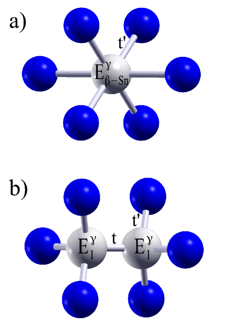
For our present electronic structure calculation, we start by considering the Ge1-xSnx alloy formed by three components: Ge, -Sn and -Sn atoms, as an effective binary alloy composed by two components: one, represented by the (Ge+-Sn) substitutional alloy as considered by Jenkins and DowJenkins , and the other component represents the -Sn non-substitutional defects. For the latter, we propose an effective substitutional 2-site cluster equivalent to the real non-substitutional -Snslafes , as illustrated in Fig. 1 and detailed in next subsection II.1. In subsection II.B we present our extension of the Jenkins-Dow TB+VCA calculation to treat the effective substitutional binary alloy representing the real alloy with Ge, -Sn and -Sn.
II.1 Effective substitutional two-site cluster equivalent to the non-substitutional -Sn defect
As mentioned above, in a previous workslafes we determined and compared two effective substitutional two-site clusters equivalent to the real non-substitutional -Sn defects: schematically represented in Fig.1. In Fig.1.(a) we depict the real non-substitutional -Sn defect ( with energy , where represents each basis orbital (), in its sixfold coordinated configuration). Meanwhile Fig.1.(b) represents an equivalent cluster composed by two substitutional sites, where the effective atoms occupying each site in the cluster have an energy denoted by (considered to be equal in both sites of the cluster, by symmetry).slafes
The equivalence was established under the following conditions: (1) for simplicity, we propose that the equivalence is valid for each separate orbital; (2) we assume that only interactions between orbitals of the same type between nearest-neighbour (NN) atoms are relevant; and (3) we demand that the local Green’s functions in the original and equivalent problems are equal, and will thus have the same analytical properties.
Due to our investigation in Ref.slafes, , no qualitative differences are expected for the electronic structure obtained using equivalent clusters with null intra-cluster hopping , or with intra-cluster hopping equal to that between the cluster and the rest of the lattice: .
Thus, in our present work we adopt the effective equivalent substitutional cluster with , to represent the -Sn non-substitutional defects. In this case, from Ref. slafes, we have:
| (1) |
The energy of the effective pseudo-atoms with the correct symmetry has been expressed in terms of energy parameters corresponding to the original -Sn defect, allowing to incorporate these non-substitutional defects in the electronic structure calculation of the alloy under study in terms of substitutional defects.
II.2 TB+VCA extension to include -Sn and non-substitutional -Sn in the Ge1-xSnx electronic structure calculation
To obtain the virtual-crystal band structure of Ge1-xSnx, including substitutional -Sn and non-substitutional -Sn, we propose the following extension for the TB+VCA approximation of the substitutional alloy originally proposed by Jenkins and Dow.Jenkins We will use the same basis of 20 tight-binding orbitals ( with , , character) introduced by Jenkins and Dow for the group IV elements, but in the diagonal part of the Hamiltonian we will add a set of three orbital weight factors, depending on the orbital character of the basis state, and take into account the presence of -Sn. Concretely, we consider the following matrix elements for the TB+VCA Hamiltonian of the binary alloy:
| (2) |
where and respectively, denote the diagonal and non-diagonal matrix elements of the Hamiltonian, subindices and refer to the TB-orbital states and denotes each Hamiltonian block with , or orbital character. Further details of the structure of this TB Hamiltonian can be found in Ref.Jenkins, . By [Ge] and [-Sn] we respectively refer to the tight-binding parameters for pure Ge or for -Sn, as given in Ref. Jenkins, . Meanwhile [-Sn] denotes the TB Hamiltonian matrix elements corresponding to the substitutional equivalent used for the real non-substitutional defect, in our case: [-Sn] = = [-Sn] + . In our present calculations, for simplicity we have assumed that a Sn-atom has the same tight-binding parameters in both configurations: -Sn and -Sn. By and we denote the relative concentration of -Sn and -Sn respectively in Ge1-xSnx, therefore: .
In the diagonal matrix elements of the Hamiltonian above, we introduced three orbital weight factors: ( = , or ), in order to reproduce as closely as posible the band structure of Ge1-xSnx alloys, according to recent experiments,Atwater ; Menendez-2006 ; gallagher2014 and in particular improve the description of the indirect to direct gap transition of the substitutional alloy w.r. to the original approach by Jenkins and Dow Jenkins . were included as factors of the Sn-atoms contribution to the diagonal matrix elements, as the pure Ge indirect (and direct) gapshandbook are correctly described by the Jenkins and Dow TB elementsJenkins . In following subsection we will discuss in detail the parametrization adopted for these parameters.
Notice that we adopt the non-diagonal Hamiltonian matrix elements of Jenkins and Dow,Jenkins which include the lattice parameters for Ge and -Sn, namely: Å, and Å, and we are assuming that Vegard’s lawvegard is valid for the binary alloy lattice parameter, thus: .
The present extension of TB+VCA enables us to tackle two important issues in Ge1-xSnx: 1) as already mentioned, a more realistic description of the crossover from indirect to direct fundamental bandgap, according to recent experiments, and 2) the inclusion of non-substitutional complex -Sn defects in the electronic structure calculation, which have been confirmed to exist by experiments, and as we will show would play an important role in the electronic properties of Ge1-xSnx, basically limiting the direct gap phase of interest for optoelectronics applications.
II.2.1 Parametrization of Wγ: indirect to direct gap transition in substitutional Ge1-xSnx
Now, we will explain how we optimized the values of the weight parameters: ( = , or ), introduced in Eq.II.2, in order to properly reproduce the available experimental data of Ge1-xSnx alloys, and in particular the critical Sn-concentration for the indirect to direct gap transition in substitutional Ge1-xSnx.
Using the original TB+VCA approach for substitutional Ge1-xSnx by Jenkins and DowJenkins one obtains that = 0.15CFB-2009 . Recently, other theoretical predictions were reported: = 0.17 was obtained with a charge self-consistent pseudo-potential plane wave methodMoontragoon2007 , = 0.11 with the empirical pseudopotential method with adjustable form factors fitted to experimental dataLow2012 , while the full potential augmented plane wave plus local orbital method within density functional theory(DFT) yielded: = 0.105.Chibane2010 Gupta et al.pseudo2013 predicted =, using a theoretical model based on the nonlocal empirical pseudopotential method. Eckhardt et al.,Eckhardt2014 predicted for Ge1-xSnx grown commensurately on Ge(100) substrates, using a supercell approach and VCA, with DFT in the local density approximation.
Our extension of the TB+VCA described in subsection II.2 includes three orbital weight parameters ( = , or ), which we introduced to improve the fit of the TB model to experimental electronic structure results. They enable us to construct a TB model to correctly reproduce the experimental data reported for the indirect and direct bandgaps of Ge and Ge1-xSnx at particular alloy concentrations.Atwater ; Menendez-2006 ; Chen2011 In our present work, we adjusted ( = , or ), using experimental data for the indirect and direct bandgaps of pure Ge () and Ge0.85Sn0.15: obtained by He and Atwater Atwater through optical absorption experiments, and confirmed nine years later by transmittance measurements by D’Costa et al.Menendez-2006 The set of optimal weight factors obtained by fitting these data are:
| (3) |
Regarding the choice of the weight factors specified in Equation 3, it was done taking into account our study of the orbital character of the eigenvectors along the Brillouin zone (BZ),slafes and in particular at the symmetry points which define the fundamental bandgap, depending on the alloy composition: namely the BZ center, , with the relevant valence band maximum, and the conduction band minimum determining the direct gap, and BZ point where the conduction band minimum determining the indirect gap in Ge lies. At , we find that the eigenvectors correspond mainly to -states at the conduction band minimum and mainly -states at the valence band maximum, while at the eigenvectors correspond mostly to -states, though a minor proportion of -character is retained, and these results do not exhibit significant changes increasing Sn-concentration. Meanwhile, increasing the energy of the valence band maximum at remains almost fixed, while it is the energies of the conduction band minima at and which are changed.slafes Based on these facts we set , and proceeded to adjust and to fit the experimental direct and indirect bandgapsAtwater ; Menendez-2006 ; Chen2011 at .
Henceforward, the set of values for specified in Eq.3 will be kept constant for all electronic structure calculations in this work. Notice that the only change to the matrix elements of the tight-binding Hamiltonian of Jenkins and DowJenkins , due to the introduction of these optimized weight factors in Eq.II.2, appears in the diagonal TB parameters for -Sn (and -Sn in our approximation), here given by: eV and eV.
In Table 1, we show a comparison between the direct and indirect bandgaps obtained with the TB+VCA approach described above and the experimental results reported in Ref. Atwater, for them. As expected, there is agreement for and , used for our fits, but at intermediate Sn concentrations, the calculated values show some deviations from the experimental ones, as discussed in next section.
| Exp. | Theory | Exp. | Theory | |
|---|---|---|---|---|
| 0.00 | 0.800 0.004 | 0.803 | 0.6700.019 | 0.670 |
| 0.06 | 0.614 0.004 | 0.613 | 0.5990.019 | 0.578 |
| 0.11 | 0.445 0.003 | 0.468 | 0.428 0.019 | 0.502 |
| 0.15 | 0.346 0.003 | 0.346 | 0.441 0.004 | 0.441 |
A considerable improvement is obtained for the predicted critical Sn-concentration for the transition from an indirect to a direct fundamental gap in Ge1-xSnx, which the present approach places in the vecinity of ( with the optimized values, specified in Eq.3). This is much closer to the recently reported experimental values detailed in the Introduction than the prediction of , obtainedCFB-2009 using the original TB+VCA by Jenkins and DowJenkins .
Finally, before discussing in detail the results obtained with our approach in next section, we would like to comment on two recent parametrizations of the tight binding parameters,Kufner2013 ; Attaoui2014 and compare them with those including spin orbit interaction and up to second-nearest neighbour effects proposed by Jenkins and Dow in 1987.Jenkins
In 2013, Küfner et al.,Kufner2013 studied the structural and electronic properties of pure -Sn nanocrystals from first principles, using DFT within approximations based on the hybrid exchange-correlation functional and including spin-orbit interaction effects. They reported a list of first-NN tight-binding parameters for -Sn with some differences with respect to those of Refs.Vogl, ; Jenkins, . Replacing in the TB+VCA approach by Jenkins and DowJenkins the first-NN tight-binding parameters of pure -Sn by those of Küfner et al.Kufner2013 , we find that the prediction for the indirect to direct gap transition in Ge1-xSnx would be shifted from CFB-2009 ; Jenkins to .
In 2014, based on the first-NN tight-binding parameters for pure Ge of Vogl et al.Vogl and those by Küfner et al. for -SnKufner2013 , Attiaoui et al.Attaoui2014 presented a semi-empirical second-NN tight-binding calculation of the electronic structure of Ge1-x-ySixSny ternary alloys as well as Ge1-xSnx. Using the same 20 basis states as Refs.Vogl, ; Jenkins, ; Kufner2013, , they evaluated new TB parameters for the alloy components, with some changes to the previous ones also including second-neighbours and spin orbit correctionsJenkins . For the indirect to direct gap transition in substitutional unstrained Ge1-xSnx they obtain , which is smaller than and agrees with the experimental data of Ref. Menendez-2006, , though it overestimates more recent experimental values mentioned in the Introduction.Chen2011 ; Menendez2012 ; gallagher2014 Concerning the electronic structure study of substitutional unstrained Ge1-x-ySixSny ternary alloys, the prediction of Ref.Attaoui2014, is consistent with previous resultsternarios obtained using an extension of the TB+VCA by Jenkins and DowJenkins . In particular, almost equal critical concentration values (with minor differences possibly related to the use of different pure Sn-lattice parameter valuesternarios ; Attaoui2014 ) are predicted for the transition of the indirect gap: between two different relevant conduction band minima defining the gap (one Ge-like at Brillouin zone point L, and the other Si-like).
III Results and discussion
Here, we will present electronic structure results obtained using our approach described in previous section, divided in two subsections. In the first one, we will discuss and compare in detail with recent experiments our results for the low Sn-concentration regime: where only substitutional -Sn is expected to be present. In the second subsection, we show our predictions for Ge1-xSnx alloys at higher Sn-concentrations where, above a temperature-dependent critical Sn-concentration, also non-substitutional -Sn defects are expected to be presentCFB-2009 ; CFB-Physica . In particular, for each of these two regimes, we discuss the fundamental gap transition of Ge1-xSnx which is expected to take place.
III.1 Substitutional alloy: results of the present approach for Ge+-Sn
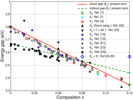
Using the TB+VCA approach described in previous section for Ge1-xSnx alloys in the low regime, where all Sn atoms occupy substitutional positions in the Ge lattice, we obtained the results exhibited in Fig. 2. There, we show the compositional dependence of the direct () and indirect () bandgaps of Ge1-xSnx obtained with the present approach, intersecting at where the indirect to direct transition of the fundamental gap is thus predicted. For comparison, we included a series of recently available experimental data,Menendez-2006 ; Atwater ; Lin-TSF2012 ; Chen2011 ; Ladron2007 ; gallagher2014 ; Chen-APL2012 and also show the indirect to direct gap transition prediction of , obtained using the original TB+VCA approach,Jenkins ; CFB-2009 which yields a gap value of 0.568 eV at that Sn-concentration, much higher than the observed fundamental direct gap of 0.346 eVAtwater detailed in Table 1.
The direct and indirect bandgaps obtained with our approach (in eV) can be respectively fitted as follows:
| (4) |
Comparing our results with the experimental data in Fig. 2, one sees that a relatively good description of the compositional dependence of the direct and indirect gaps is obtained, indeed much better than if a linear interpolation between the respective gap values for pure Ge and -Sn was used.Atwater ; Menendez-2006 ; Chen2011 Nevertheless, small deviations from linearity in the data are evident,Atwater ; Menendez-2006 ; Menendez-2011 as experimentally reported also for the lattice constant of Ge1-xSnxMenendez-2011 . Many other binary semiconducting alloys AxB1-x also exhibit similar non-linear dependences of their physical properties as a function of alloy composition, behaviour known as bowing effects. Though VCA cannot describe non-linear bowing effects, it nevertheless often yields good qualitative results.Menendez-2006
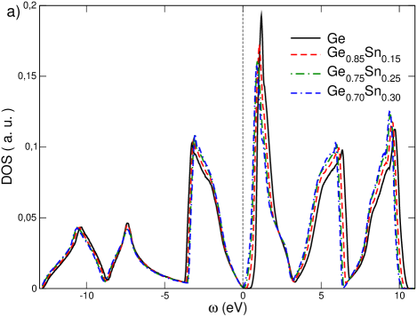
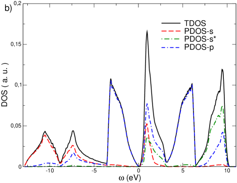
Fig.3(a) shows the total density of states obtained for Ge1-xSnx as a function of energy, at substitutional-Sn concentrations: . In agreement with the results obtained using the ab-initio FPLO5+CPA codeKoepernik in Ref.CFB-2009, , notice that a smooth behaviour as function of Sn concentration is obtained, with changes in the bandwidth, and a progressive reduction of the gap around the with Sn concentration. Experiments in Ge1-xSnxAtwater ; Menendez-2006 ; Ladron2007 ; Chen2011 ; Chen-APL2012 confirmed that the direct gap decreases primarily through a Sn-content increase in the alloy.Atwater ; Menendez-2002 ; Menendez-2006
In Fig. 3(b), we show the total and the three partial densities of states as a function of energy for Ge0.78Sn0.22 substitutional alloy. Around the bandgap two peaks are visible in the density of states: the peak located just below the gap is clearly dominated by orbital contributions, while and orbitals contribute to the peak located just above the gap. Moreover, we can see that the lowest band ( -12 eV) corresponds essentially to orbitals, while the highest band ( 10 eV) is originated essentially by and orbitals, as in pure Ge. These features also agree with the FPLO5+CPA resultsCFB-2009 ; Koepernik .
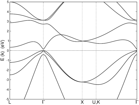
In Fig. 4, we show the band structure obtained for the substitutional Ge0.78Sn0.22 alloy. In order to analyze the fundamental bandgap in Ge1-xSnx, we focus on three specific BZ points which define it: the maximum of the valence band at , the minima of the conduction band at and at , with energies denoted , and respectively. Notice that Ge0.78Sn0.22 possesses a fundamental direct gap : 0.132 eV , and as indirect gap: 0.334 eV . Moreover, analyzing the orbital-character of the band structure: we found that the eigenvectors corresponding to and , are mainly due to and states, respectively. Meanwhile, the eigenvectors at are due to and states. These results are analogous to those obtained for pure Ge, which indicates that the relative weights of the orbital contributions to the electronic properties of Ge1-xSnx are weakly dependent of Sn-content in the substitutional alloy.
III.2 Ge1-xSnx: TB+VCA results including -Sn and -Sn, metallization transition
In previous section, we showed that Ge1-xSnx possesses an indirect fundamental gap at low Sn-concentrations, and that by increasing Sn-concentration the substitutional binary alloy undergoes a crossover from an indirect to a direct bandgap at . At higher Sn-concentrations, non-substitutional -Sn defects appear in the binary alloy, as predicted theoreticallyCFB-Physica ; CFB-2009 and confirmed by experiments decoster . We will now show that the presence of -Sn reduces the concentration range where Ge1-xSnx possesses a direct gap, i.e. it reduces the critical concentration at which the direct gap closes, corresponding to the metallization transition.
We analyzed the effect of both substitutional and non-substitutional Sn defects on the electronic structure of Ge1-xSnx employing the TB+VCA extension proposed in the present work, detailed in Section II.
.
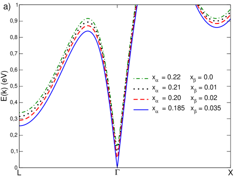
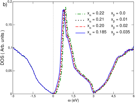
To assess the effect of -Sn defects on the electronic structure, in particular, on the bandgaps, in Fig. 5(a), we plot the TB+VCA band structure of Ge0.78Sn0.22 along the Brillouin zone path, for a fixed total Sn-concentration , but different relative contents of -Sn and non-substitutional -Sn. Notice that when increases, for example from 0 to 0.035, the bandgap decreases: a progressive reduction of the direct gap at upon increase of the -Sn concentration is observed. In Fig. 5(b), we show the effect of -Sn upon the DOS, for fixed total Sn-concentration and varying the relative -Sn content in the alloy. The changes induced by increasing -Sn concentration on the density of states are less noticeable than those obtained in the band structure (see Fig. 5(a)). The progressive reduction of the gap confirms that the presence of non-substitutional -Sn favours the metallization in Ge1-xSnx.
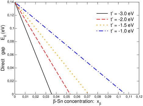
In Fig. 6 we plot the direct gap energy , for the binary alloy with fixed total Sn-concentration as a function of ( i.e. ), for four different values of hopping between Sn and its Ge nearest-neighbours. A linear dependence of as a function of is obtained. The critical concentration at which the direct gap closes, and the alloy becomes metallic, is strongly dependent on in our approach.
Analyzing the effect of non-substitutional -Sn on the total and partial densities of states, using our TB+VCA approach we find that the relative weights of the orbital contributions to the electronic properties of Ge1-xSnx are weakly dependent of Sn-content.
Experimentally, the critical Sn-concentration for the metallization transition in Ge1-xSnx is yet unknown. As shown in Fig.2 gap measurements were reported at relatively low Sn-concentrations: Atwater ; Menendez-2006 ; Low2012 ; Chen2011 ; Lin2011 ; Ladron2007 . More recently, the direct gap was determined in homogeneous epitaxial layers of Ge1-xSnx grown on InP substrates Nakatsuka2013 for , from photon absorption spectra measured with Fourier transform infrared spectroscopy. In particular, for Ge0.73Sn0.27 Nakatsuka et al.Nakatsuka2013 obtained a direct gap of 0.25 eV, so that the metallization of these epitaxial layers would occur at .
Additional measurements for higher Sn-concentrations would be required to locate the metallization transition in bulk Ge1-xSnx. Extrapolating experimental data fits, two predictions for were obtained: by Atwater et al.Atwater , and by V.R. D’Costa et al.Menendez-2006
On the other hand, Jenkins and Dow predicted Jenkins with their original TB+VCA approach for substitutional Ge1-xSnx. If we would consider only substitutional -Sn to be present and use our present TB+VCA extension, we would predict for the transition from a direct gap to a metallic regime: , same value which can be obtained if using the TB parameters for -Sn reported in Ref. Kufner2013, .
In 2009 we proposed a statistical model for the formation of -Sn defects in Ge1-xSnx, CFB-Physica ; CFB-2009 from which the relative concentrations of -Sn ( and -Sn) in the alloy can be obtained as a function of temperature and the total Sn-concentration .
Using the statistical model CFB-Physica ; CFB-2009 to determine in Ge1-xSnx ( and from it: ) , we can explore the dependence of the critical concentration for metallization on the only free parameter () in our present approach. Furthermore, if were experimentally known, it might be used to tune the free parameter . In Figure 7 we address this issue, by plotting corresponding to values in the range from to for different temperatures . Specifically for T = 16 ∘C, 32 ∘C, 62 ∘C, 85 ∘C and 131 ∘C, while the relative contents and are obtained from the statistical modelCFB-Physica ; CFB-2009
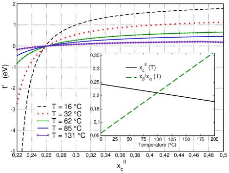
Figure 7 shows that for , is negative and increases monotonically with increasing . On the other hand, for , is positive. Note that, all of these graphs in Fig. 7 intersect at , which corresponds to : which in our model is equivalent to considering only substitutional Sn to be present.
For instance, if we consider the temperature C, by adjusting eV we would obtain a value , as suggested extrapolating the experiments of Ref. Atwater, , while, if we consider the same temperature but adjust eV, we would obtain a value , as suggested by extrapolating the experiments of Ref. Menendez-2006, .
The inset of Figure 7 depicts, for , the temperature dependence obtained in our approach for the critical concentration for metallization, (full line), and for the ratio between the non-substitutional -Sn and the substitutional -Sn (dashed line) concentrations at from Refs.CFB-Physica, ; CFB-2009, . The inset reveals an increase in as a function of temperature, while a decrease in as a function of temperature is observed. These results indicate that increasing the non-substitutional Sn content leads to a lower , i.e. confirming that the presence of -Sn favours metallization.
As we mentioned in the Introduction, the main interest for technological applications of Ge1-xSnx is linked to its direct gap phase.Menendez-2002 ; Menendez-2006 However, our results show that the concentration range (), in which Ge1-xSnx possesses a direct fundamental gap would be reduced if the temperature of formation of the alloy is increased, since -Sn might appear at lower Sn-concentrations. An important aspect in the fabrication of high-quality thin films using molecular beam epitaxy is the growth-temperatureMenendez-2002 ; Menendez-2006 ; Menendez-APL2011 ; Menendez-APL2010 . Therefore, a detailed experimental study of the electronic properties of these alloys, including the second gap transition (metallization), could allow to determine the optimal growth conditions to control the proportion of -Sn in Ge1-xSnx.
IV Conclusions
We have studied the effect of -Sn non-substitutional complex defects on the electronic structure of the Ge1-xSnx binary alloy.
In order to include non-substitutional complex defects in an electronic structure calculation, we presented our extension of the method originally proposed by Jenkins and Dow for substitutional Ge1-xSnx, using 20 tight-binding orbitals for the group IV elements combined with the virtual crystal approximation. We included the complex non-substitutional -Sn defects through the introduction of an effective substitutional two-site equivalent cluster for them, which we appropriately embedded in the lattice to calculate the electronic structure of the effective alloy purely in terms of substitutional defects.
Our method allows to describe the two transitions of the fundamental gap of Ge1-xSnx as a function of the total Sn concentration. In particular: i) with our proposed extension for the tight-binding matrix, we could tune the critical Sn concentration for the transition from an indirect to a direct gap, in agreement with the most recent experimental data. Our extension also improves the theoretical description of the direct gap experimental values for ternary Ge1-x-ySixSny alloys, as shown in the Appendix. ii) The metallization transition ( closure of the direct gap) of Ge1-xSnx at higher can also be described, and we demonstrated the relevance of non-substitutional -Sn for the determination of . In fact, if would be measured it could be used to determine the hopping parameter () between -Sn defects and the Ge matrix, only free parameter of our model. iii) We predict the effect of temperature on the metallization transition (not yet experimentally measured), resulting from the increase with temperature of the ratio between the concentrations of non-substitutional to substitutional Sn in Ge (which we obtain from our statistical model for Ge1-xSnx).
We believe that the physical properties of Ge1-xSnx are strongly affected by Sn complex defects in the Ge matrix , such as -Sn among othersCFB-2009 , and future experimental work would provide further support and increase the usefulness of the present approach. Furthermore, the general idea we proposed to include non-substitutional complex defects in electronic structure calculations, by determining effective substitutional equivalent clusters to replace them and solve the problem in terms of purely substitutional effective alloys, has a wide potential for applications in other systems.
V Acknowledgments
C.I.V. and J.D.F. are Investigadores Científicos of CONICET (Argentina). J.D.Q.F. has a fellowship from CONICET. C.I.V. acknowledges support for this work from CONICET (PIP 0702) and ANPCyT (PICT’38357; PICT Redes’1776), and R.A.B. from CONACyT project 179616.
Appendix A Application to Ge1-x-ySixSny ternary alloys
In 2013 we reported a first calculation of the electronic structure of Ge1–x–ySixSny ternary alloysternarios , employing a combined TB+VCA approximation method which we developed as a direct extension to ternary substitutional alloys of the Jenkins and Dow approach Jenkins for binary substitutional Ge1-xSnx. The same problem was later studied also in Ref.Attaoui2014, .
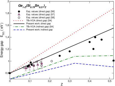
Our electronic structure results for ternary Ge1–x–ySixSny confirmed predictions and experimental indications that a 1 eV bandgap was attainable with these alloys, as required for the fourth layer planned to be added to present-day record-efficiency triple-junction solar cells, in order to further increase their efficiency for satellite applications.
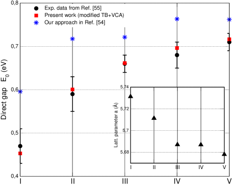
It is interesting to apply the present TB+VCA parametrization for the substitutional alloy discussed in Section II.2.1 of the present work, in particular the renormalized Sn tight-binding parameters, as starting point to recalculate the electronic structure of the ternary alloys and compare it with the results of our previous calculation ternarios . We exhibit the comparison of the direct gap results as a function of composition in Figs. 8 and 9 . In Fig. 8 one sees how the parametrized TB+VCA approach of the present work improves the description of the experimental compositional dependence of the direct gap w.r. to our previous approach of Ref.ternarios, for a series of samples lattice-matched to Ge, while we also show how the predicted indirect gap is slightly modified. In Fig. 9 we compare our present parametrized TB+VCA results for the direct gap with recent experimental resultschi2013 for five ternary alloys with different lattice parameters ( shown as inset): within the experimental error bars the agreement is indeed very good for all samples, greatly improved w.r. to the direct gap values predicted by the previous TB+VCA approachternarios .
References
- (1) M. R. Bauer, J. Taraci, J. Tolle, A. V. G. Chizmeshya, S. Zollmen et al., Appl. Phys. Lett. 81, 2992 (2002).
- (2) R. Hull and J. C. Bean, Germanium Silicon: Physics and Materials, Semiconductors and Semimetals, (Academic, San Diego, 1999).
- (3) C. H. L. Goodman, IEE Proc. Part I: Solid-State Electron Devices Lett. 129, 189 (1982).
- (4) V. R. D’Costa, C. S. Cook, A. G. Birdwell, C. L. Littler, M. Canonico, S. Zollner, J. Kouvetakis J, and J. Menendez, Phys. Rev. B 73, 125207 (2006).
- (5) C. C. Yeo, B. J. Cho, F. Gao, S. J. Lee, M. H. Lee, C. Y. Yu, C. W. Liu, L. J. Tang, and T. W. Lee, IEEE Electron Device Lett. 26, 761 (2005).
- (6) Y. J. Yang, W. S. Ho, C. F. Huang, S. T. Chang, and C. W. Liu Appl. Phys. Lett. 91, 102103 (2007).
- (7) G. He and H. A. Atwater, Phys. Rev. Lett. 79, 1937 (1997). R. Ragan, K. S. Min, and H. A. Atwater, Mater. Sci. Eng. B. 87, 204 (2001).
- (8) J. D. Sau, and M. L. Cohen, Phys. Rev. B 75, 045208 (2007).
- (9) Lei Lui, Renrong Liang, Jing Wang, and Jun Xu, Appl. Phys. Expr. 8, 031301 (2015).
- (10) E. Kasper, M. Oehme, T. Arguirov, J. Werner, M. Kittler, and J. Schulze, Advances in Optoelectronics 2012, 916275 (2011).
- (11) W. Du, S. A. Ghetmiri, B. R. Conley, A. Mosleh, et al., Appl. Phys. Lett. 105, 051104 (2014).
- (12) J. D. Gallagher, C. L. Senaratne, P. M. Wallace, J. Menéndez, and J. Kouvetakis, Appl. Phys. Lett. 107, 123507 (2015).
- (13) L. Viña, H. Höchst, and M. Cardona, Phys. Rev B 31, 958 (1985).
- (14) O. Gurdal, R. Desjardins, J. R. A. Carlsson, N. Taylor, H. H. Radamson, J. E. Sundgren, and J. E. Greene, J. Appl. Phys. 83, 162 (1998).
- (15) H. Lin, R. Chen, Y. Huo, T. I. Kamins, and J. S. Harris, Thin Solid Films 520, 3927 (2012).
- (16) R. Chen, H. Lin H, and Y. Huo et al., Appl. Phys. Lett. 99, 181125 (2011).
- (17) G. Grzybowski, R. T. Beeler, L. Jiang, D. J. Smith, and J. Kouvetakis, et al., Appl. Phys. Lett. 101, 072105 (2012).
- (18) W. Wegscheider, J. Olajos, U. Menczigar, U. Dondl, and G. Abstreiter, J. Cryst. Growth 132, 75 (1992).
- (19) O. Nakatsuka, Y. Shimura, W. Takeuchi, N. Taoka, and S. Zaima, Solid State Electron. 83, 82 (2013).
- (20) H. Pérez Ladrón de Guevara, A. G. Rodríquez, H. Navarro-Contreras et al., Appl. Phys. Lett. 91, 161909 (2007).
- (21) M. -Y. Ryu, T. R. Harris, Y. K. Yeo, R. T. Beeler, and J. Kouvetakis, Appl. Phys. Lett. 102, 171908 (2013).
- (22) W.-J. Yin , X.-G. Gong , and S.-H. Wei, Phys. Rev. B 78, 161203 (2008).
- (23) J. D. Gallagher, C. L. Senaratne, J. Kouvetakis, and J. Menéndez. Appl. Phys. Lett. 105, 142102 (2014).
- (24) L. Jiang, C. Xu, J. D. Gallagher, R. Favaro, T. Aoki, José Menéndez, and J. Kouvetakis. Chem. Mater., 26, 2522 (2014).
- (25) C. I. Ventura, J. D. Fuhr and R. A. Barrio, Physica B 404, 2830 (2009).
- (26) C. I. Ventura, J. D. Fuhr, and R. A. Barrio, Phys. Rev B 79, 155202 (2009).
- (27) S. Decoster, S. Cottenier, U. Wahl, J. G. Correia, and A. Vantomme, Phys. Rev. B 81, 155204 (2010).
- (28) I. Chambouleyron, F. Marques, P. H. Dionisio, I. J. R. Baumvol, and R. A. Barrio, J. Appl. Phys. 66, 2083 (1989).
- (29) J. D. Fuhr, C. I. Ventura, and R. A. Barrio, J. Appl. Phys. 114, 193508 (2013), and refs. therein.
- (30) D. W. Jenkins and J. D. Dow Phys. Rev. B 36, 7994 (1987).
- (31) K. E. Newman and J. D. Dow, Phys. Rev. B 30, 1929 (1984).
- (32) D. J. Chadi, Phys. Rev. B 16, 790 (1977).
- (33) D. J. Chadi, and M. L. Cohen, Phys. Stat. Solid. (b) 68, 405 (1975).
- (34) D. J. Chadi, and M. L. Cohen, Phys. Rev. B 7, 692 (1973).
- (35) R. A. Barrio, J. D. Querales Flores, J. D. Fuhr, and C. I. Ventura, J.of Superc. and Novel Magn. 26, 2213 (2013); J. D. Querales Flores, Master in Physics Thesis, Instituto Balseiro (2010).
- (36) L. Vegard, Die Konstitution der Mischkristalle und die Raumfüllung der Atome. Zeitschrift für Physik 5, 17-26 (1921).
- (37) P. Moontragoon, Z. Ikonic and P. Harrison, Semiconductor Science and Technology 22, 742 (2007).
- (38) K. L. Low, Y. Yang, G. Han, W. Fan, and Y. C. Yeo, J. Appl. Phys. 112, 103715 (2012).
- (39) Y. Chibane, and M. Ferhat, J. Appl. Phys. 107, 053512 (2010).
- (40) S. Gupta, B. Magyari-Köupe, Y. Nishi, K. Saraswat, J. Appl. Phys. 113, 073707 (2013).
- (41) C. Eckhardt , K. Hummer , and G. Kresse, Phys. Rev. B 89, 165201 (2014).
- (42) R. Beeler, R. Roucka, A. V. G. Chizmeshya, J. Kouvetakis, and J. Menéndez, Phys. Rev.B 84, 035204 (2011).
- (43) S. Küfner, J. Furthmüller, et al. Phys. Rev. B 87, 235307 (2013).
- (44) A. Attiaoui, and O. Moutanabbir, J. Appl. Phys. 116, 063712 (2014).
- (45) P. Vogl, H. P. Hjalmarson, and J. D. Dow, J. Phys. Chem. Solids 44, 365 (1983).
- (46) F. Gencarelli, D. Grandjean, Y. Shimura, et al., J. Appl. Phys. 117, 095702 (2015).
- (47) O. Madelung, Semiconductors - Basic Data (Springer, Berlin, 1996).
- (48) K. Koepernik, and H. Eschrig, Phys. Rev. B 59, 1743 (1999); I. Opahle, K. Koepernik, and H. Eschrig Phys. Rev.B 60, 14035 (1999); K. Koepernik, R. Velicky, R. Hayn, and H. Eschrig Phys. Rev. B 55, 5717 (1997).
- (49) A. S. Carrico, R. J. Elliot, and R. A. Barrio, Phys. Rev. B 34, 872 (1986).
- (50) J. Avendaño López, F. L. Castillo Alvarado, and R. A. Barrio, Revista Mexicana de Física 40, 750 (1994).
- (51) H. Lin, R. Chen, W. Lu, Y. Huo, T. I. Kamins, et al., Appl. Phys. Lett. 100, 102109 (2012).
- (52) H. Lin, R. Chen, Y. Huo, et al., Appl. Phys. Lett. 98, 261917 (2011).
- (53) R. Roucka, J. Mathews, R. T. Beeler, J. Tolle, J. Kouvetakis, et al., Appl. Phys. Lett. 98, 061109 (2011).
- (54) J. Mathews, R. T. Beeler, J. Tolle, C. Xu, R. Roucka,et al., Appl. Phys. Lett. 97, 221912 (2010).
- (55) C. I. Ventura, J. D. Querales Flores, J. D. Fuhr, and R. A. Barrio, Prog. Photovolt: Res. Appl. 23, 112 (2015). ( Published online: 6 Aug. 2013 - DOI: 10.1002/pip.2405).
- (56) Chi Xu, Liying Jiang, John Kouvetakis and José Menéndez, Appl. Phys. Lett. 103, 072111 (2013).
- (57) V. R. D’ Costa, Y. Y. Fang, J. Kouvetakis and J. Menéndez, Phys. Rev. Lett. 102, 107403 (2009).
- (58) R. T. Beeler, C. Xu, D. J. Smith, G. Grzybowski, J. Menéndez, J. Kouvetakis, et al., Appl. Phys. Lett. 101, 221111 (2012).
- (59) C. Xu, R.T. Beeler, G. J. Grzybowski, A.V.G Chizmeshya, et al., J. Am. Chem. Soc. 134, 20756 (2012).