The Effective Model of the Molecule Graphene System and One Application beyond Graphene
Abstract
Recently, a new kind of two dimensional (2D) artificial electron lattice, i.e. molecule graphene, has drawn a lots of interest, where the metal surface electrons are transformed into a honeycomb lattice via absorbing a molecule lattice on metal surfaceGomes et al. (2012); Wang et al. (2014). In this work, we would like to point out that the technique used to build molecule graphene actually gives a promising way to explore the interesting physics of other novel 2D lattice beyond graphene. The key issue is that this system is an antidot system, where the absorbed molecule normally gives a repulsive potential. So, we need to establish a map between the molecule arrangement and the desired surface electron lattice. To give a concrete example, we first analyse the effective models of molecule graphene, and estimate the model parameters for the Cu/CO system through numerical fitting the exerimental data. Then, we design a molecule lattice, and show that, with this kind of lattice, the surface electrons can be transformed into a Kagome like lattice. Using the estimated parameters of Cu/CO system, we calculate the corresponding energy bands and LDOS, which can be readily tested in experiment. We hope that our work can stimulate further theoretical and experimental interest in this novel artificial 2D electron lattice.
I Introduction
Recently, a novel kind of artificial two dimensional (2D) electronic lattice, named molecule graphene, has been successfully realized on metal surface in order to mimic the Dirac like linear dispersion of grapheneGomes et al. (2012); Wang et al. (2014). In experimentGomes et al. (2012), CO molecules are absorbed on Cu(111) surface and then assembled into a hexagonal lattice by the tip of scanning tunneling microscopy (STM). The surface has a Shockley surface state near the Fermi level, which can be viewed as a two dimensional electron gas with dispersion. Meanwhile, each absorbed molecule applies a local potential on the surface states, and thus the molecule lattice is equivalent to a lateral periodic potential, which transforms the surface electrons into an artificial honeycomb latticePark and Louie (2009).
Artificial 2D lattice systems are always the research focus during the last two decades, because that it not only relates to the fundamental physics about 2D system, but also has potential for application. The nano-patterned semiconductor 2DEG, cold atom, and the photonic crystal are the well-known artificial 2D lattice systems, which have been intensively studied. Here, the metal surface state patterned by the absorbed molecules offers a new artificial 2D lattice system, where molecule graphene is first example realized in experiment. This new artificial 2D system has its own characteristic and merits. First, it is a 2D electron lattice in solid state system in contrast to the cold atom and photonic crystal systems, so that the electron-electron interaction can be included naturally. Moreover, because the 2D electrons are the surface states, the STM gives a powerful detecting method, which not only can measure the DOS, LDOS, but also could get the accurate information about the edge statesWang et al. (2014), charge order, the spin order (by spin-polarized STMWiesendanger (2009)), and even the quasi particle energy (by inelastic electron tunnelling spectroscopy). These critical information can not be easily detected in other artificial 2D lattice systems. Considering these great advantages, this new artificial 2D lattice system deserves more research efforts.
So far, all the investigations about the molecule graphene system (i.e. metal surface electrons patterned by absorbed molecule lattice) are mainly focused on the physics of graphene, e.g. the linear dispersionGomes et al. (2012); Ropo et al. (2014); Hammar et al. (2013); Feilhauer et al. (2015), edge and impurity statesWang et al. (2014), finite size effect(Aichinger et al., 2014), topological nontrivial phasesde Juan (2013); Ghaemi et al. (2012) and superconductivityGao et al. (2014). However, it should be noticed that this powerful technique actually provides a promising method to study interesting physics in any 2D electron lattice, not just the graphene lattice. To the best of our knowledge, there are still few works to discuss the possibility to construct other novel 2D lattices on metal surface by this technique. One critical issue is that, like the Cu/CO system, the absorbed molecule normally applies a repulsive potential on the metal surface state, so that it is an antidot system. To get a desired 2D lattice of surface electrons, we need to design a special molecule arrangement, and thus numerical simulation with realistic parameters becomes indispensable.
In this work, we first theoretically analyse the two effective models of the molecule graphene used in literatures, discuss their relation and differences. By numerical simulation and comparing with the experimental data, we estimate the parameters of different effective models for the Cu/CO system, which is an ideal system to construct 2D lattice of surface electron. We point out that the potential value of the absorbed CO molecules in the muffin-tin model is of the order of several eV, which is a critical parameter to simulate other 2D lattice in Cu/CO system. Then, with these estimated parameters, we give an interesting example which can be readily tested in experiment. We design a 2D molecule lattice and show that, with this kind of molecule arrangement, we can get a band structure rather similar to that of Kagome lattice, which is of special interest in condensed matter physics. We hope that our work can stimulate further theoretical and experimental interests in this promising artificial 2D electronic lattice system.
The paper is organized as following: In Sec. II, we discuss the two effective models of molecule graphene, and estimate the parameters of the effective models for the Cu/CO system; In Sec. III, we design a molecule arrangement and show that it can give a Kagome like band structure via numerical simulation; Finally, we give a summary in Sec. IV.
II Effective models of molecule graphene
Basically, the molecule graphene is one kind of artificial graphene, which was first proposed in the semiconductor 2DEG system(Park and Louie, 2009; Gibertini et al., 2009; Polini et al., 2013). In the literatures, except the DFT calculationRopo et al. (2014), two effective models using different potential models are used to describe such artificial graphene system. For the artificial graphene, they both work and are equivalent in some sense. However, only the effective model with muffin-tin potential is a general model which is applicable to all the 2D lattice. In addition, we emphasize that the potential values of the two effective models are of different physical meanings, and of different order of magnitude. Sometimes, they are confused in literatures since which effective model is used is not declared.
In order to do a realistic simulation for other 2D lattices, we first need to get some critical parameters of the Cu/CO system by analysing the effective models and the experimental results of the molecule graphene. Here, we only focus on the Cu/CO system, since it has been realized in experiment and is an ideal system to build other 2D lattice. For other systems, e.g. other moleculesWang et al. (2014), simulation can be done in the same way.
II.1 Two Potential Models
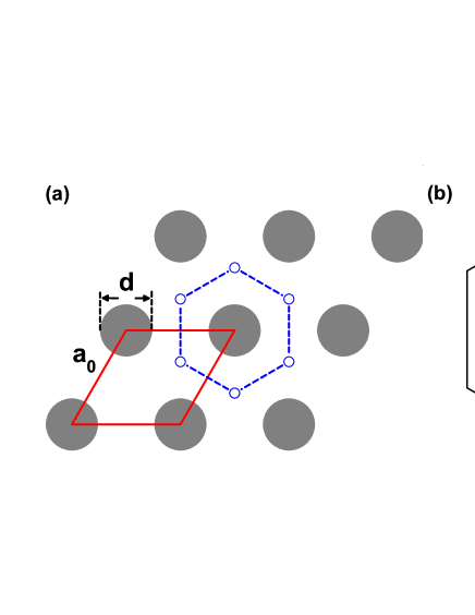
To describe the molecule graphene system, the Cu(111) surface state is approximately considered as a 2DEG. When the absorbed molecule lattice is formed, it exerts a lateral periodic potential on the surface electrons. So far, in the literatures, there are two kinds of potential models used to simulate the lateral periodic potential. One is the muffin-tin potential modelPark and Louie (2009); Wang et al. (2014), as shown in Fig. 1. The Hamiltonian of the whole system is
| (1) |
where the muffin-tin potential is inside the gray disks and zero elsewhere, is the effective mass of the Cu(111) surface state, and the Fermi energy relative to the band bottom is meV. To calculate the energy bands, we can expend the Hamiltonian with the plane wave basis and get the central equations
| (2) |
and are the reciprocal lattice in momentum space, is the coefficient of the plane wave and is the Fourier component of the muffin-tin potential. As shown in Fig. 1 (a), there are three parameters for the muffin-tin potential: the lattice constant of the molecule lattice , the diameter of the potential disk and the potential value . We can get an analytical expression about the Fourier component of the muffin-tin potential
| (3) |
Here, is the unit cell area of the molecule lattice, is the Bessel function. Given the muffin-tin potential, we can get the energy bands of the molecule graphene by solving the central equations above. The Dirac like linear dispersion is only related with the lowest three bands.
The other potential model for the molecule graphene is actually a simplification of the muffin-tin potential. When calculating the energy bands with the central equations, it is shown that, for the molecule graphene case, the first Fourier component dominates, where , and are the basis of reciprocal lattice. Thus, in some theoretical literatures, only the terms are considered as the potential model to simulate the molecule graphene, which we call the model hereGomes et al. (2012); Polini et al. (2013); Nádvorník et al. (2012). The benefit of the model is that there is now only one potential parameter, i.e. the value of , for the band calculation instead of the two in the muffin-tin potential case ( and ). Note that the molecule distance is the same in any potential models. So, it is convenient to use the model for both the numerical calculation and the fitting of the experiment. We want to emphasize here that when we talk about the potential value of molecule graphene system, it should be aware of which potential model is used. Otherwise, it is easier to confuse and , since they all have the dimension of energy and are both named as potential value.
The disadvantage of the model is that it is not transferable for studying other 2D lattice, which is one of the main purposes of this work. On one side, there is no direct relation between the terms of different 2D lattices, even if the same molecules are used. On the other side, for some 2D lattices, only including the terms is not enough to correctly describe the energy bands. It should be noticed that the muffin-tin potential model is naturally applicable for all kinds of 2D lattice, though it is not as convenient as the model for the experiment fitting since more potential parameters are involved. Once we get the parameters of the muffin-tin potential in the Cu/CO system, it can be straightforwardly used to simulate the case of other 2D lattice.
For convenience, in the following, we will first use the model to fit the experimental data of the molecule graphene in Cu(111)/CO system. Then, with Eq. 3, we estimate the parameters of the muffin-tin potential, which is applicable to other 2D lattice. Finally, using the muffin-tin potential, we give an interesting example in next section.
II.2 Numerical Simulation
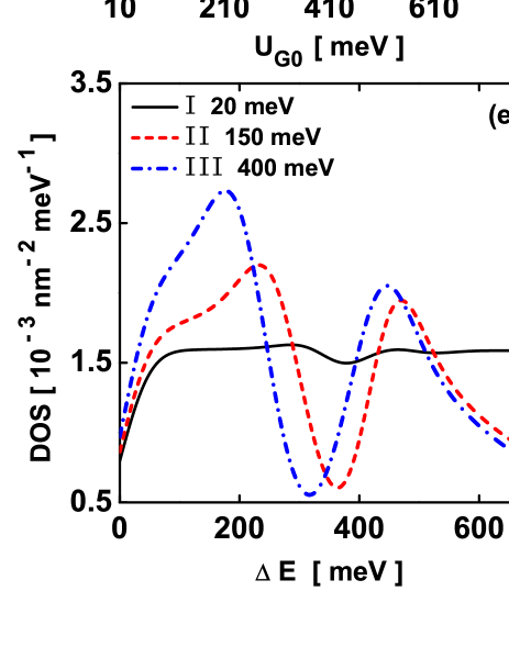
Let us first discuss the experimental results of the molecule graphene in Cu(111)/CO system. In experiment, the molecule graphene is identified by measuring the graphene like DOS, as well as the honeycomb LDOS pattern, with STMGomes et al. (2012); Wang et al. (2014). Thus, in our calculation, we only focus on the simulation about the DOS with the effective model, while the band structure of the molecule graphene has been discussed in detail in former literaturesPark and Louie (2009); Nádvorník et al. (2012). Without the absorbed molecules, the Cu surface states can be approximately viewed as a 2DEG with a parabolic dispersion, the DOS of which is about . Note that the DOS of pure Cu surface states is used to scale the DOS of the molecule graphene in experimentGomes et al. (2012). The detail DOS data of the molecule graphene is given in Ref. 1 with molecule lattice constant nm (see the Fig. 1 of the supplementary material of Ref. 1). The DOS shape of the molecule graphene is similar as that of graphene, where the DOS minimum is near the Dirac point and two DOS peaks are near the two Van Hove singularities below and above the Dirac point, respectively. Beyond the common features, the observed DOS of molecule graphene has some quantitatively characteristics: (1) the amplitude of the DOS peaks, , where () is the DOS value of the lower (upper) DOS peak relative to the Dirac point. is the minimum of the DOS near the Dirac point; (2) the two DOS peaks are asymmetry. The ratio is about ; (3) the relative energy positions of the two peaks, meV and meV, where , , are the energy of the lower DOS peak , the upper DOS peak, the DOS minimum, respectively. Then, based on the effective model of molecule graphene, we would like to see in which parameter region the calculated DOS can reproduce the experimental results.
For the DOS calculation, the life time broadening of the energy level, resulting from the scattering between the surface electrons and bulk states, is a crucial quantity because that it determines the magnitude of DOS value. In experiment, it is estimated that the energy broadening is about meV in Cu(111)/CO systemGomes et al. (2012).
Now, we discuss the numerical results of the model, from which we want to estimate the reasonable value of by comparing with the experimental DOS data. In Fig. 2 (a), we plot the DOS of the molecule graphene as a function of ( nm), where is the energy relative to the band bottom. A typical DOS is shown in Fig.2 (b), which is like that of graphene. In order to do quantitative comparisons, we plot the amplitude of the two DOS peaks, as well as their ratio , in Fig. 2 (c) as a function of . Meanwhile, the relative energy position of the two DOS peaks are also given in Fig. 2 (d). According to these data, we can roughly identify three distinct regions as indicated in Fig. 2 (a), and we plot the typical DOS curves in the three regions in Fig. 2 (e). In small region (Region I), the amplitude of the DOS peaks are tiny, which is qualitatively inconsistent with the experiment [the black solid line in Fig. 2 (e)]. In moderate region (Region II), the amplitude of the two DOS peaks becomes larger and is comparable to the experimental value, but the two DOS peaks are nearly symmetrical [the red dashed line in Fig. 2 (e)]. The asymmetry ration R is around 1, which is also qualitatively different from the experimental observation. Only if the is large enough, we can get a reasonable DOS shape, which is qualitatively in agreement with the experimental observation. However, from the DOS data above, we can not get a satisfied quantitative fitting with this effective model, which can exactly reproduce the experimental data. For example, if the amplitude of first DOS peak is exactly equal to the experimental value, the should be in the moderate region and give a symmetrical DOS shape. Meanwhile, in the large region, the relative position of the two peaks are about 20 meV larger than the experimental value (from 20 meV to 30 meV depending on value).
Considering all the numerical results above, we suggest that, for the molecule graphene in Cu/CO system, the acceptable region of is between 400 meV to 600 meV. Only if is in this region, we can get a reasonable DOS shape, while the peak amplitude, peak position and asymmetry ratio is comparable to the experimental value. Two important issues should be made clear further. One is that, in former studies, the value is estimated by the energy difference between the M point and Dirac point in the BZ, and it is argued that is about 100 meVGomes et al. (2012); Polini et al. (2013). However, when the life time broadening is considered in the DOS calculation, it is obvious that the DOS peaks are not at the M point and the DOS minimum is also shifted from the Dirac point. That is why the value suggested here is larger than the former one. We plot the DOS with suggested values in Fig. 2 (f). The other is that even in this region, there is still a difference about 20 meV between the experimental and theoretical values of the position of the DOS peaks. We argue that this discrepancy may result from the assumption about the life time broadening, where it is considered as a constant in our calculation. Actually, the life time broadening of the metal surface states has been intensively studied, and normally it is a function of energyEiguren et al. (2002). To get a better effective model is still an open question and need further efforts in future.
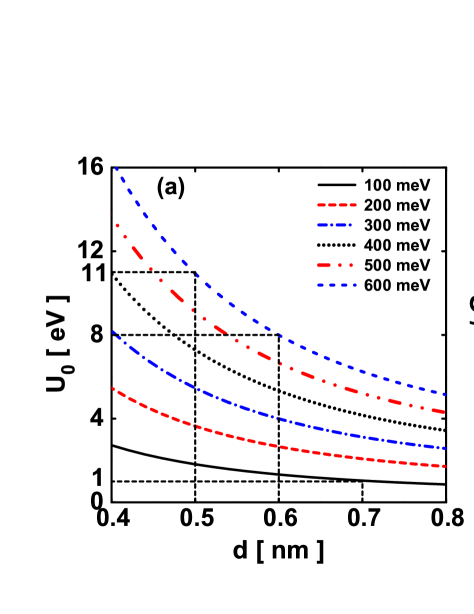
We then estimate the parameters of the muffin-tin potential with Eq. 3. Except the lattice constant , which is controlled in experiment, the muffin-tin potential model has two parameters: potential value and diameter . Given , the Eq. 3 indicates that is a function of . In Fig. 3 (a), we plot as a function of for different values. According to the charge difference got by DFT calculation, the potential diameter of the CO molecule should be in the region between 0.5 nm to 0.7 nmRopo et al. (2014). As indicated in Fig. 3 (a), we can see that the should be in the region between 4 eV and 10 eV. Note that the is larger than 1 eV even if meV. Thus, it is safely to say that the of muffin-tin potential is of several eV for the Cu/CO system, which is the central result for this section. Here, we give some further evidence from the related quantum corral system to support our estimation aboveFiete and Heller (2003); Harbury and Porod (1996); Rahachou and Zozoulenko (2004). In the well-known quantum corral system, adatoms (e.g Fe atoms) are absorbed on Cu(111) surface to form a corral, which confines the surface electrons and gives rise to a standing wave pattern in the corral. Similar as the molecule graphene, each adatom applies a local potential on the surface electrons. By fitting the experiment, it is suggested that the potential value of the adatom is about several eVHarbury and Porod (1996); Rahachou and Zozoulenko (2004). Together with our calculation, we believe that our estimation about the is reasonable. Note that the potential value are different for different molecules. Our estimation is only applicable for the Cu/CO system. In the following, we assume using Cu/CO system by default, and use eV and nm for further study, the DOS of which is plotted in Fig. 3 (b).
III An example: Artificial Kagome lattice
In last section, we discuss the effective model of molecule graphene. For the Cu/CO system, we estimate the reasonable value for and , which is applicable to all the 2D lattice. In this part, we would like to give an interesting example which is beyond the scope of graphene physics. We design a 2D molecule lattice, and by simulation with muffin-tin model, we show that this 2D lattice can mimic the band structure of Kagome lattice. As well known, the Kagome lattice is of highly interests in condensed matter physics because of its novel correlated ground stateMielke (1992); Yan et al. (2011); Jo et al. (2012); Zheng et al. (2014). So far, in solid state electron system, a clean Kagome lattice, as simple as graphene, has not been found. Our scheme may offer a novel platform to study the physics of Kagome lattice.
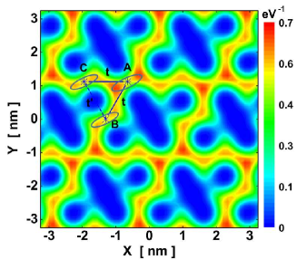
The molecule arrangement we designed is shown in Fig. 4 (a), where each gray disk represents a molecule and the unit cell is indicated by the red line. The basic idea is simple. First, we arrange the molecules to form a hexagonal lattice. If we assume that each lattice site of the surface electron is positioned at the inner of diamond formed by four adjacent molecules, we then get a same hexagonal lattice for the surface electrons. It should be noted that if one quarter of the lattice sites is deleted, the hexagonal lattice can be transformed into the Kagome lattice. Thus, we use an additional molecule to “kill” one lattice site, as shown in Fig. 4 (a). There are three sites in one unit cell of the Kagome lattice, which is marked by the blue stars in Fig. 4 (a) (A, B, C sites). Meanwhile, the nearest neighbourhood hopping are denoted as and , where the hopping between B and C sites () is different from that between A and B (). The corresponding Kagome lattice is given in Fig. 4 (c).
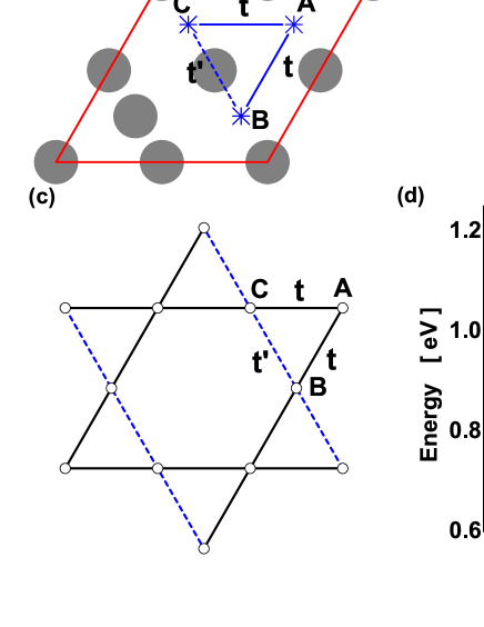
We then use the muffin-tin potential with the parameters of Cu/CO system estimated above to simulate the artificial Kagome lattice system. The lowest three bands are plotted in Fig. 4 (d) (the black solid line). We try to use a tight binding model to fit the calculated band, and the results are plotted in Fig. 4 (d) (the red dotted line). The tight binding Hamiltonian is
| (4) |
where is the index of unit cell, indicates the three different sites in one unit cell and denotes the electron spin. is the hopping terms
| (5) |
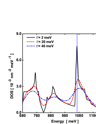
where denotes the nearest neighbourhood hopping. In spite of our best efforts, we only get a qualitatively fitting about the energy bands, which is not as good as the case of molecule graphene. The parameters are meV, meV, meV and meV. The numerical simulation demonstrates that the molecule structure we designed can be roughly viewed as a Kagome lattice with non-equal nearest neighbourhood hopping. The corresponding DOS is given in Fig. 5 with different life time broadening. For Kagome lattice, one of the three bands is very flat, and thus induce a giant DOS peak (see in Fig. 5), which may induce interesting correlated electronic states in experiment. Meanwhile, the Fermi level is controllable by adjusting the molecule distance .
The main reason for the discrepancy between the tight binding bands and the ones got by plane wave method is because that each site of the surface electrons here has inner electron structure. This can be seen from the LDOS of this Kagome lattice, as shown in Fig. 6. In each site, e.g. the B site, the electron distribution is not uniform, and seems to be composed of two small sites. However, we try several possible tight bind models and do not get a better approximation. Anyway, ignoring the detailed inner electronic structure in each site, the LDOS can be viewed as a Kagome lattice, which is consistent with the energy band calculation and can be described by the tight binding model above. Since in our simulation we use the realistic parameters of Cu/CO system, we believe that the Kagome lattice structure proposed here can be easily tested in experiment.
IV conclusion
In summary, the purpose of this work is to point out that the technique used to build molecule graphene in recent experiments offers a new opportunity to explore the novel physics in any 2D lattice beyond the scope of graphene. To demonstrate this idea, we first analyze the effective models of the molecule graphene. We discuss the relation and distinction between the two potential models used to simulate the molecule graphene. Then, by fitting the DOS data, we estimate the parameters for each potential model in the Cu/CO system. We point out that, for the muffin-tin potential, potential value is of the order of several eV and potential diameter is between 0.5 and 0.7 nm, which can be used to simulate any other 2D molecule lattice in the Cu/CO system. Finally, we give an interesting example. We design a molecule lattice, and by numerical simulation we show that this molecule arrangement can give a Kagome like band structure. Note that in experiment there are two ways to build a molecular lattice on metal surface. One is by the STM tips, as discussed above. The other is to use the self-assembly process, where organic porous networks are used to confine the surface electronsLobo-Checa et al. (2009); Wang et al. (2013). However, it is still a big challenge to build a complex 2D lattice of surface electron by the self-assembly technique, though it is useful to make a molecule network in a large area.
The molecule graphene represents a new kind of artificial 2D electron lattice system, which has its own advantages compared with other artificial 2D lattice systems, e.g. the cold atom, nano-patterned 2DEG in semiconductor, and photonic crystal. It of course will not only limited to the graphene system, but also can be used to study any novel 2D lattice. From the success of molecule graphene, we believe that the technique is now ready. But it should be noted that the molecule graphene is a quantum antidot system. To build the desired 2D lattice, we need a map from the molecule arrangement to the 2D surface electron lattice we want. That is what we do in this work. Our scheme here give a theoretical proposal to get a Kagome like 2D lattice. And the estimation about the model parameters of the Cu/CO system also gives a basis for future numerical simulation. We hope that our work can stimulate more research interest into this new artificial 2D lattice system, and believe that it will lead to new experimental progress in near future.
Acknowledgements.
This work is supported by the National Science Foundation of China (Grants No. 11274129, No. 11534001).References
- Gomes et al. (2012) K. K. Gomes, W. Mar, W. Ko, F. Guinea, and H. C. Manoharan, Nature 483, 306 (2012).
- Wang et al. (2014) S. Wang, L. Z. Tan, W. Wang, S. G. Louie, and N. Lin, Phys. Rev. Lett. 113, 196803 (2014).
- Park and Louie (2009) C.-H. Park and S. G. Louie, Nano Letters 9, 1793 (2009).
- Wiesendanger (2009) R. Wiesendanger, Rev. Mod. Phys. 81, 1495 (2009).
- Ropo et al. (2014) M. Ropo, S. Paavilainen, J. Akola, and E. Räsänen, Phys. Rev. B 90, 241401 (2014).
- Hammar et al. (2013) H. Hammar, P. Berggren, and J. Fransson, Phys. Rev. B 88, 245418 (2013).
- Feilhauer et al. (2015) J. Feilhauer, W. Apel, and L. Schweitzer, Phys. Rev. B 92, 245424 (2015).
- Aichinger et al. (2014) M. Aichinger, S. Janecek, I. Kylänpää, and E. Räsänen, Phys. Rev. B 89, 235433 (2014).
- de Juan (2013) F. de Juan, Phys. Rev. B 87, 125419 (2013).
- Ghaemi et al. (2012) P. Ghaemi, S. Gopalakrishnan, and T. L. Hughes, Phys. Rev. B 86, 201406 (2012).
- Gao et al. (2014) J.-H. Gao, Y. Zhou, and F.-C. Zhang, arXiv:1412.0337 [cond-mat] (2014), arXiv: 1412.0337.
- Gibertini et al. (2009) M. Gibertini, A. Singha, V. Pellegrini, M. Polini, G. Vignale, A. Pinczuk, L. N. Pfeiffer, and K. W. West, Phys. Rev. B 79, 241406 (2009).
- Polini et al. (2013) M. Polini, F. Guinea, M. Lewenstein, H. C. Manoharan, and V. Pellegrini, Nature Nanotechnology 8, 625 (2013).
- Nádvorník et al. (2012) L. Nádvorník, M. Orlita, N. A. Goncharuk, L. Smrcka, V. Novák, V. Jurka, K. Hruska, Z. Výborný, Z. R. Wasilewski, M. Potemski, and K. Výborný, New Journal of Physics 14, 053002 (2012).
- Eiguren et al. (2002) A. Eiguren, B. Hellsing, F. Reinert, G. Nicolay, E. V. Chulkov, V. M. Silkin, S. Hüfner, and P. M. Echenique, Phys. Rev. Lett. 88, 066805 (2002).
- Fiete and Heller (2003) G. A. Fiete and E. J. Heller, Rev. Mod. Phys. 75, 933 (2003).
- Harbury and Porod (1996) H. K. Harbury and W. Porod, Phys. Rev. B 53, 15455 (1996).
- Rahachou and Zozoulenko (2004) A. I. Rahachou and I. V. Zozoulenko, Phys. Rev. B 70, 233409 (2004).
- Mielke (1992) A. Mielke, Journal of Physics A 25, 4335 (1992).
- Yan et al. (2011) S. Yan, D. A. Huse, and S. R. White, Science 332, 1173 (2011).
- Jo et al. (2012) G.-B. Jo, J. Guzman, C. K. Thomas, P. Hosur, A. Vishwanath, and D. M. Stamper-Kurn, Phys. Rev. Lett. 108, 045305 (2012).
- Zheng et al. (2014) L. Zheng, L. Feng, and W. Yong-Shi, Chinese Physics B 23, 077308 (2014).
- Lobo-Checa et al. (2009) J. Lobo-Checa, M. Matena, K. Müller, J. H. Dil, F. Meier, L. H. Gade, T. A. Jung, and M. Stöhr, Science 325, 300 (2009).
- Wang et al. (2013) S. Wang, W. Wang, L. Z. Tan, X. G. Li, Z. Shi, G. Kuang, P. N. Liu, S. G. Louie, and N. Lin, Phys. Rev. B 88, 245430 (2013).