Experimental approval of the extended flat bands and gapped subbands in rhombohedral multilayer graphene
Abstract
Graphene layers are known to stack in two stable configurations, namely ABA or ABC stacking, with drastically distinct electronic properties. Unlike the ABA stacking, little has been done to experimentally investigate the electronic properties of ABC graphene multilayers. Here, we report the first magneto optical study of a large ABC domain in a graphene multilayers flake, with ABC sequences exceeding 17 graphene sheets. The ABC-stacked multilayers can be fingerprinted with a characteristic electronic Raman scattering response, which persists even at room temperatures. Tracing the magnetic field evolution of the inter Landau level excitations from this domain gives strong evidence to the existence of a dispersionless electronic band near the Fermi level, characteristic of such stacking. Our findings present a simple yet powerful approach to probe ABC stacking in graphene multilayer flakes, where this highly degenerated band appears as an appealing candidate to host strongly correlated states.
Tailoring the electronic and optical properties of layered materials by controlling the layer orientation or their stacking order is an important possibility offered by the physics of two dimensional systems. Graphene is the first isolated two dimensional crystal Novoselov et al. (2004) and the properties of graphene stacks, from mono- to multi-layers (N-LG), have been intensively investigated in the last decade Castro Neto et al. (2009). The thermodynamically stable stacking of multilayer graphene is the Bernal stacking, where the A sublattice in one layer comes right below the B sublattice in the other layer Koshino (2013). It was not until recently that experiments on rhombohedral stacking, with an ABC layer sequence, have been reported. ABC tri-layer graphene, the simplest rhombohedral N-LG, have been successfully isolated and presents a tunable band gap Lui et al. (2011) as well as chiral quasi-particles as evidenced from their unconventional quantum Hall effect Bao et al. (2011); Zhang et al. (2011); Kumar et al. (2011).
To our knowledge, there are yet no investigations of ABC graphene multilayers. This is mainly because of the low abundance of this polytype in real samples. Hence, tracing the evolution of the electronic properties of ABC-stacked multilayers when increasing the number of layers remains challenging. One of the intriguing predictions about electronic properties of ABC-stacked multilayers is that they are expected to host surface states (localized mainly on the top and bottom layers) with a flat dispersion near the corners of the Brillouin zone, and bulk states with a band gap. When increasing the number of ABC-stacked layers, the extend of the flat dispersion of the low energy bands increases, while the size of the bulk band gap decreases Burkov et al. (2011); Xiao et al. (2011).

Notably, the surface states of ABC-stacked graphene multilayers have been reported as topologically protected, due to the symmetry of this material Xiao et al. (2011), and may thus resemble those well-known surface states of 3D topological insulators Hsieh et al. (2008); Zhang et al. (2009); Hasan and Kane (2010); Qi and Zhang (2011). Interestingly, due to weak spin-orbit interaction in carbon-based systems, an even closer analogy is found with the surface states of topological crystalline insulators Fu (2011). Nevertheless, in contrast to these two families of topological insulators, the bulk band gap of ABC-stacked graphene multilayers gradually closes with the increasing number of atomic sheets and bulk rhombohedral graphite may behave as a 3D topologically protected semimetal Ho et al. (2016). The expected high degeneracy of the flat bands could lead to exotic electronic ground states, such as magnetically ordered phases or surface superconductivity Muñoz et al. (2013); Kopnin et al. (2013); Olsen et al. (2013). Experimental signatures of this flat bands has been recently observed in scanning tunnelling spectroscopy (STS) and angular-resolved photo emission spectroscopy (ARPES) investigations of nanometer scale domains of ABC-stacked graphene multilayers (5 layers) grown on 3C-SiC Pierucci et al. (2015).
In this Letter, we demonstrate, using Raman scattering techniques, that ABC-stacked multilayers () can be found within exfoliated N-LG flakes. They have characteristic signatures in their Raman scattering response, which allow for their identification at room temperature. These signatures include a change of the 2D band feature line shape Chiu et al. (2011), together with an additional Raman scattering feature which we attribute to electronic Raman scattering (ERS) across the band gap in the bulk. ABC-stacked domains can thus be identified by spatially mapping the Raman scattering response of different flakes. Experiments performed with an applied magnetic field () reveal two distinct series of electronic inter Landau level excitations, involving the low energy surface flat bands, and the bulk gapped states, respectively. Experimental results are explained in the frame of a tight binding (TB) model of the electronic band structure of rhombohedral N-layer thin graphite layers Min and MacDonald (2008); Yuan et al. (2011).

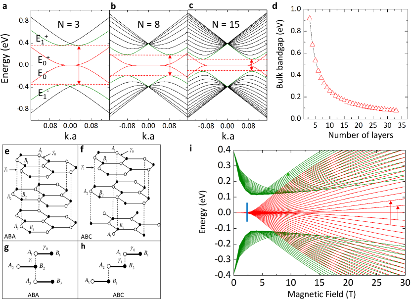
The 7 parameters TB model developed by Slonczewski-Weiss and McClure McClure (1957); Slonczewski and Weiss (1958) for bulk graphite can be simplified by only considering the two first intra- and inter- nearest neighbors hopping parameters and , respectively (Figure 1f-i). The calculated low energy band structure of ABC N-LG is shown in Figure 1a-c, for and layers. Two characteristic evolutions when increasing the number of ABC-stacked layers arise from these calculations: (i) the flat part of the low energy bands (red bands in Figure 1a-c) extends over a larger -space region, and (ii) the energy separation between the (green bands in Figure 1a-c), decreases and ultimately closes for rhombohedral graphite (see Figure 1d).
A natural way of exploring electronic band structures of solids is to apply a magnetic field in order to induce Landau quantization, and to trace the evolution of inter Landau level excitations with a magneto-spectroscopy techniques, such as magneto-Raman scattering spectroscopy. The evolution with magnetic field of the four lowest in energy bands of a ABC stacked sequence is presented in Figure 1e. One can note that Landau levels are formed from the flat bands (red lines), and that their energies grow nearly linearly with the magnetic field, but starting from a finite onset magnetic field. For , the onset field is close to T, as indicated by blue bar in Figure 1e. As a consequence, inter-Landau level excitations within the flat bands (red arrows), in the first approximation, evolve linearly with the applied magnetic field, however with a rather unusual extrapolated negative energy offset (see supplementary information). We anticipate that this will be the magneto-Raman scattering signature of electronic states with such dispersion. Landau levels in the and bands (green lines in Figure 1e) also show a non trivial evolution when increasing the magnetic field. From eV at the K-point, their energies first decrease (increase) with the magnetic field until they reach , respectively. For higher magnetic fields, their energies increase (decrease) with a quasi linear evolution. Thus, inter Landau level excitations involving these states (green arrows) are expected to first decrease in energy down the gap value, and to grow in a linear way for higher magnetic fields.
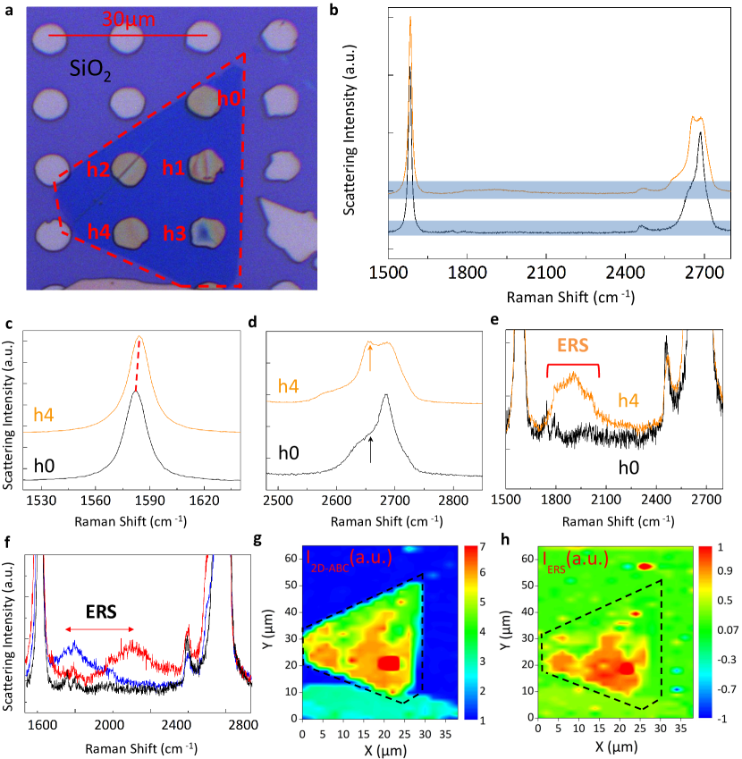
An optical photograph of the investigated flake is presented in Figure 2a. The flake is produced from the mechanical exfoliation of bulk graphite and transferred on a SiO2(90nm)/Si substrate patterned with holes in the oxide (see Methods). The Raman scattering signal from the suspended parts is enhanced due to an optical interference effect in the substrate Yoon et al. (2009); Li et al. (2012). The N-LG flake covers five different holes labelled h0 to h4, where it is suspended. The flake has been characterized by atomic force microscopy (AFM) measurements which indicate a thickness of 15 to 17 layers (see supplementary information). Raman scattering spectra are then measured at room temperature with 50x objective and a nm laser excitation, or at liquid helium temperature in a solenoid using a homemade micro-magneto-Raman scattering (MMRS) spectroscopy set-up with a nm laser excitation (see Methods). In both experiments, piezo stages are used to move the sample with respect to the laser spot and to spatially map the Raman scattering response of the flake, or to investigate specific locations.
Two characteristic Raman scattering spectra measured at h0 (black curve) and at h4 (orange curve) are presented in Figure 2b. One can recognize on these spectra the characteristic phonon response of sp2 carbon, including the G band feature around cm-1, and the 2D band feature observed around cm-1 when measured with nm excitation. If the spectrum measured at h0 corresponds to that of thin AB-stacked layers Faugeras et al. (2008), the spectrum measured at h4 is notably different, even though the thicknesses of the layer at these two locations are similar: i) the G band energy at h4 is blue shifted by cm-1 with respect to that measured at h0 (Figure 2c, ii) the 2D band line shape is more complex with two additional contributions indicated by arrows in 2d, and iii) an additional broad feature (Figure 2e is observed at h4 around 1805 cm-1 with a full width at half maximum (FWHM) of cm-1. These are the three main Raman scattering signatures of ABC-stacked graphene multilayers.

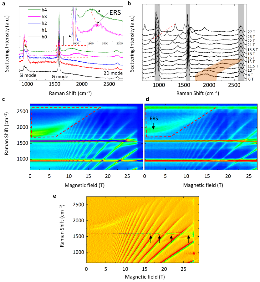
To study the homogeneity of the N-LG flake, we have performed spatial mappings of the Raman scattering response at room temperature, with m spatial steps. When scanning the surface of the flake, it appears that the broad Raman scattering feature is observed in a large domain and that its central position can change from one location to another (see Figure 2f). As will be clarified in the following by the magneto-Raman measurements, we interpret this feature as arising from an electronic excitation between two bands of the band structure of ABC N-LG. Similar to metallic carbon nanotubes Farhat et al. (2011) and bulk graphite Ponosov et al. (2015), electronic excitations do contribute to the room temperature Raman scattering response of ABC-stacked N-LG. The different locations on the flake where this ERS signal is observed are presented in the form of a false color spatial map in Figure 2h. The modified line shape of the 2D band is also observed at different locations on our flake, shown in Figure 2g. The correlation between these two false color maps is a strong indication that the observation of the ERS feature and of the modified 2D band line shape are signatures of the same, ABC stacking. This flake is hence composed of two distinct domains: the first is ABA-stacked, and is extending over h0, h1 and h2, while the other is ABC-stacked, extending over h3 and h4. The energy of this ERS (i.e., the bulk band gap in Figure 1a-c depends on the number of ABC-stacked layers, and, taking the extreme values of the ERS energy from the measured Raman spectra all over the ABC domain, we estimate the number of ABC-stacked graphene layers to vary from to over the whole flake. This feature is also observed at low temperature, as can be seen in Figure 3a.

Characteristic MMRS spectra measured at h4 are presented in Figure 3b, for different values of B. The central position of the broad ERS feature increases with increasing magnetic field and its intensity seems to vanish for T. The fact that magnetic fields can influence so much the energy and amplitude of this feature is in line with an electronic origin for this excitation. Above T a series of sharp features, dispersing with the magnetic field, appears in the Raman scattering response. They have a symmetric line shape, in contrast to electronic excitations observed in bulk graphite Kossacki et al. (2011).
The evolution of the Raman scattering response with magnetic field, measured at h3 and h4, are presented in Figures 3c-d, respectively, in the form of false color maps of the scattered intensity. These two locations show a similar response. The observed electronic excitation spectrum in magnetic field is composed of a series of features linearly dispersing with increasing magnetic field and of the ERS observed at , that acquires a fine structure at finite . The linearly dispersing features, in line with magneto-Raman scattering selection rules in graphene Kashuba and Fal’ko (2009) or in graphite Kossacki et al. (2011), can be attributed to symmetric (, where n is the Landau level index) inter Landau level excitations within the bands and they represent the strongest contribution to the electronic Raman scattering spectrum in magnetic field. Optical-like excitations () are not directly seen but they effectively couple to the G band. They give rise to the magneto-phonon resonance and to the associated anti-crossings when they are tuned in resonance with the G band energy Ando (2007); Kashuba and Fal’ko (2009). Such anti-crossings are indicated by red arrows in the B-differentiated color map of h4, presented in Figure 3f. The detailed analysis of the magneto-phonon resonance in ABC N-LG is beyond the scope of this paper. Of much weaker intensity, Raman scattering features with an energy decreasing when increasing the magnetic field are observed (red marked regions in Figure 3d-e. These features are better seen in Figure 3e, that shows the subtracted false color map of h3. They correspond to symmetric () inter Landau level excitations within the lowest bands in the bulk. The energy of such excitations first decreases with the magnetic field as long as the Landau levels are confined in the cone of the corresponding band structure at (Figure 1c) and then, when the inter Landau level energy spacing reaches the value of the energy gap in the bulk, they merge with the broad ERS feature.
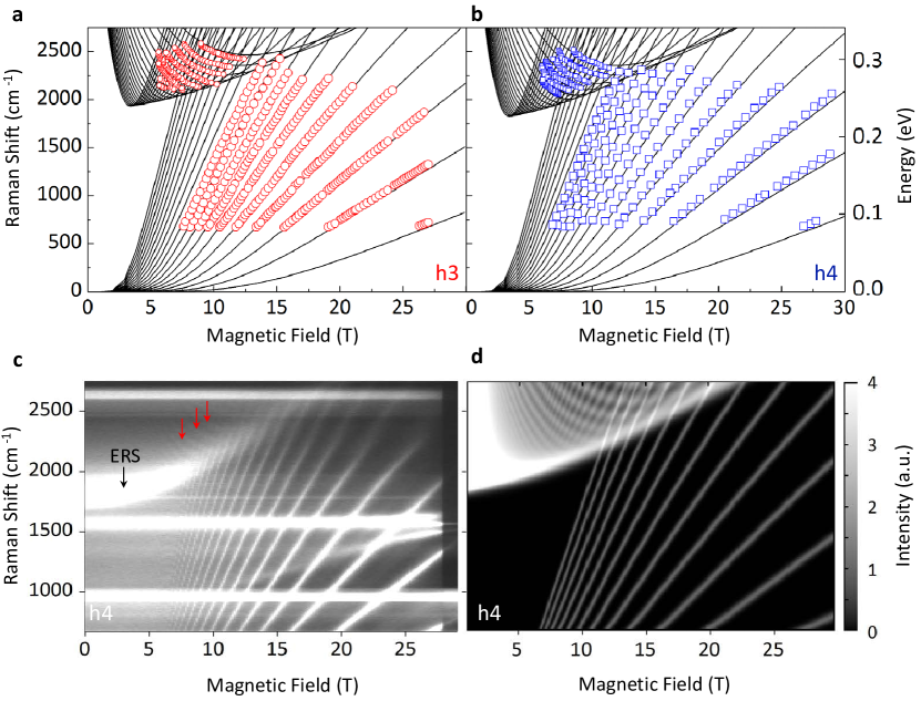
The evolution of these two families of electronic excitations with increasing magnetic field is grasped by our tight-binding analysis. We first determined the central positions of the different observed excitations using Lorentzian functions, and searched for the parameters entering the model to best describe our data. From this modelling, we can determine the number of layers to be and for h3 and h4, respectively (Figures 4a-b), while we set eV and eV, as observed in bulk graphite Nakao (1976); Kossacki et al. (2011); Kühne et al. (2012); Berciaud et al. (2014). In a simple approach (see supplementary information), we calculated the electronic excitation spectrum Kashuba and Fal’ko (2009, 2012); Mucha-Kruczyński et al. (2010) and its evolution when applying a magnetic field. These results are compared to the experimental evolution in Figures 4c-d for h4. The model reproduces the main observed features. In particular, the electronic excitation observed at is reproduced and arises indeed from an inter band electronic excitation that loses its spectral weight when the magnetic field is increased, transforming into inter Landau level excitations with their characteristic negative energy dispersion.
We report the observation of electronic excitations in N-LG system, which includes a large domain of ABC-stacked layers. The analysis of its low energy electronic excitations with magnetic field can be understood in the frame of a tight-binding model with three parameters, the number of ABC-stacked layers and the intra- and inter-layer nearest neighbors hopping integrals and . Such stacking has a unique signature in its Raman scattering response at , in the form of a low energy electronic excitations across the band gap in the bulk. The ERS response is also observed at room temperature. The central position of the ERS is related to the number of ABC-stacked layers which can then be deduced using simple Raman scattering spectroscopy. Our findings underscore the rich physics hidden in graphene multilayers with ABC stacking, namely the existence of electronic bands with a flat dispersion (diverging density of states) localized on the surface, and of electronic states in the bulk with an energy gap that depends on the number of layers. These results represent an impetus for other studies targeting the highly correlated surface states, which may lead to emergent exotic electronic ground states on this system, such as magnetic order or superconductivity.
Acknowledgements.
This work has been supported by the ERC Advanced Grant MOMB (contract no. 320590) and the EC Graphene Flagship (project no. 604391). H.P.O.C., G.U. and C.A.B. acknowledge financial support from PICTs 2013-1045 and Bicentenario 2010-1060 from ANPCyT, PIP 11220110100832 from CONICET and grant 06/C415 from SeCyT-UNC.I Methods
The measured flake was obtained from the mechanical exfoliation of natural graphite. It was then transferred non-deterministically on top of a undoped SiO2(90nm)/Si substrate on top of which an array of holes (m diameter) was etched by means of optical lithography techniques. Room temperature Raman characterization is performed on the flake, using a helium-neon laser source of nm (i.e., eV). To probe the Landau levels dispersion in our ABC N-LG flake, we used an experimental set-up comprising a homemade micro-Raman probe that operates at low temperatures and high magnetic fields. The excitation source was provided by a solid state Titanium doped sapphire laser. The excitation wavelength fixed at nm (i.e., eV) is brought to the sample by a m core mono-mode optical fiber. The end of the Raman probe hosts a miniaturized optical table comprising a set of filters and lenses in order to clean and focalize the laser spot. A high numerical aperture lens is used to focalize the laser light on the sample, which is mounted on XYZ piezo stages, allowing us to move the sample relative to the laser spot with sub-m accuracy. The non-polarized backscattered light is then injected into a 50 m multi-mode optical fiber coupled to a mono-chromator equipped with a liquid nitrogen cooled charge coupled device (CCD) array. The excitation laser power was set to 1 mW and focused onto a m diameter spot. The resulting intensity is sufficiently low to avoid significant laser induced heating and subsequent spectral shifts of the Raman features. The probe is then placed in a resistive magnetic equipped with a liquid He cryostat at 4 K. The evolution of the Raman spectrum with magnetic field was then measured on the freestanding parts by sweeping the values of the magnetic field. Each spectra was recorded for a T in order to avoid any significant broadening of the magnetic dependent features line-widths. The details of the theoretical description of the LLs and the magneto-Raman spectrum are given in the supplementary information.
References
- Novoselov et al. (2004) K. S. Novoselov, A. K. Geim, S. Morozov, D. Jiang, Y. Zhang, S. Dubonos, , I. Grigorieva, and A. Firsov, Science 306, 666 (2004).
- Castro Neto et al. (2009) A. Castro Neto, F. Guinea, N. Peres, K. S. Novoselov, and A. K. Geim, Rev. Mod. Phys. 81, 109 (2009).
- Koshino (2013) M. Koshino, New J. Phys. 15, 015010 (2013).
- Lui et al. (2011) C. H. Lui, Z. Li, K. F. Mak, E. Cappelluti, and T. F. Heinz, Nat. Phys. 7, 944 (2011).
- Bao et al. (2011) W. Bao, L. Jing, J. Velasco Jr, Y. Lee, G. Liu, D. Tran, B. Standley, M. Aykol, S. Cronin, D. Smirnov, et al., Nat. Phys. 7, 948 (2011).
- Zhang et al. (2011) L. Zhang, Y. Zhang, J. Camacho, M. Khodas, and I. Zaliznyak, Nat. Phys. 7, 953 (2011).
- Kumar et al. (2011) A. Kumar, W. Escoffier, J. M. Poumirol, C. Faugeras, D. P. Arovas, M. M. Fogler, F. Guinea, S. Roche, M. Goiran, and B. Raquet, Phys. Rev. Lett. 107, 126806 (2011).
- Burkov et al. (2011) A. Burkov, M. Hook, and L. Balents, Phys. Rev. B 84, 235126 (2011).
- Xiao et al. (2011) R. Xiao, F. Tasnadi, K. Koepernik, J. Venderbos, M. Richter, and M. Taut, Phys. Rev. B 84, 165404 (2011).
- Hsieh et al. (2008) D. Hsieh, D. Qian, L. Wray, Y. Xia, Y. S. Hor, R. Cava, and M. Z. Hasan, Nature 452, 970 (2008).
- Zhang et al. (2009) H. Zhang, C.-X. Liu, X.-L. Qi, X. Dai, Z. Fang, and S.-C. Zhang, Nat. Phys. 5, 438 (2009).
- Hasan and Kane (2010) M. Z. Hasan and C. L. Kane, Rev. of Mod. Phys. 82, 3045 (2010).
- Qi and Zhang (2011) X.-L. Qi and S.-C. Zhang, Rev. of Mod. Phys. 83, 1057 (2011).
- Fu (2011) L. Fu, Phys. Phys. Lett. 106, 106802 (2011).
- Ho et al. (2016) C.-H. Ho, C.-P. Chang, and M.-F. Lin, Phys. Rev. B 93, 075437 (2016).
- Muñoz et al. (2013) W. Muñoz, L. Covaci, and F. Peeters, Phys. Rev. B 87, 134509 (2013).
- Kopnin et al. (2013) N. Kopnin, M. Ijäs, A. Harju, and T. Heikkilä, Phys. Rev. B 87, 140503 (2013).
- Olsen et al. (2013) R. Olsen, R. van Gelderen, and C. M. Smith, Phys. Rev. B 87, 115414 (2013).
- Pierucci et al. (2015) D. Pierucci, H. Sediri, M. Hajlaoui, J.-C. Girard, T. Brumme, M. Calandra, E. Velez-Fort, G. Patriarche, M. Silly, G. Ferro, et al., ACS Nano 9, 5432 (2015).
- Chiu et al. (2011) C.-W. Chiu, Y.-C. Huang, F.-L. Shyu, and M.-F. Lin, App. Phys. Lett. 98, 261920 (2011).
- Min and MacDonald (2008) H. Min and A. MacDonald, Phys. Rev. B 77, 155416 (2008).
- Yuan et al. (2011) S. Yuan, R. Roldán, and M. I. Katsnelson, Phys. Rev. B 84, 125455 (2011).
- McClure (1957) J. McClure, Phys. Rev. 108, 612 (1957).
- Slonczewski and Weiss (1958) J. Slonczewski and P. Weiss, Phys. Rev. 109, 272 (1958).
- Yoon et al. (2009) D. Yoon, H. Moon, Y.-W. Son, J. S. Choi, B. H. Park, Y. H. Cha, Y. D. Kim, and H. Cheong, Phys. Rev. B 80, 125422 (2009).
- Li et al. (2012) S.-L. Li, H. Miyazaki, H. Song, H. Kuramochi, S. Nakaharai, and K. Tsukagoshi, ACS nano 6, 7381 (2012).
- Faugeras et al. (2008) C. Faugeras, A. Nerrière, M. Potemski, A. Mahmood, E. Dujardin, C. Berger, and W. De Heer, App. Phys. Lett. 92, 011914 (2008).
- Farhat et al. (2011) H. Farhat, S. Berciaud, M. Kalbac, R. Saito, T. F. Heinz, M. S. Dresselhaus, and J. Kong, Phys. Rev. Lett. 107, 157401 (2011).
- Ponosov et al. (2015) Y. S. Ponosov, A. Ushakov, and S. Streltsov, Phys. Rev. B 91, 195435 (2015).
- Kossacki et al. (2011) P. Kossacki, C. Faugeras, M. Kühne, M. Orlita, A. Nicolet, J. Schneider, D. Basko, Y. I. Latyshev, and M. Potemski, Phys. Rev. B 84, 235138 (2011).
- Kashuba and Fal’ko (2009) O. Kashuba and V. I. Fal’ko, Phys. Rev. B 80, 241404 (2009).
- Ando (2007) T. Ando, T. J. Phys. Soc. Jpn. 76, 024712 (2007).
- Nakao (1976) K. Nakao, T. J. Phys. Soc. Jpn. 40, 761 (1976).
- Kühne et al. (2012) M. Kühne, C. Faugeras, P. Kossacki, A. Nicolet, M. Orlita, Y. I. Latyshev, and M. Potemski, Phys. Rev. B 85, 195406 (2012).
- Berciaud et al. (2014) S. Berciaud, M. Potemski, and C. Faugeras, Nano Lett. 14, 4548 (2014).
- Kashuba and Fal’ko (2012) O. Kashuba and V. I. Fal’ko, New J Physics 14, 105016 (2012).
- Mucha-Kruczyński et al. (2010) M. Mucha-Kruczyński, O. Kashuba, and V. I. Fal’ko, Phys. Rev. B 82, 045405 (2010).