Dissipation engineering of high-stress silicon nitride nanobeams
Abstract
High-stress Si3N4 nanoresonators have become an attractive choice for electro- and optomechanical devices. Membrane resonators can achieve quality factor () - frequency () products exceeding Hz, enabling (in principle) quantum coherent operation at room temperature. String-like beam resonators possess conventionally 10 times smaller products; however, on account of their much larger -to-mass ratio and reduced mode density, they remain a canonical choice for precision force, mass, and charge sensing, and have recently enabled Heisenberg-limited position measurements at cryogenic temperatures. Here we explore two techniques to enhance the -factor of a nanomechanical beam. The techniques relate to two main loss mechanisms: internal loss, which dominates for large aspect ratios and MHz, and radiation loss, which dominates for small aspect ratios and MHz. First we show that by embedding a nanobeam in a 1D phononic crystal, it is possible to localize its flexural motion and shield it against radiation loss. Using this method, we realize MHz modes with , consistent with internal loss and contrasting sharply with unshielded beams of similar dimensions. We then study the products of high-order modes of mm-long nanobeams. Taking advantage of the mode-shape dependence of stress-induced ‘loss-dilution’, we realize a MHz mode with Hz. Our results can extend room temperature quantum coherent operation to ultra-low-mass 1D nanomechanical oscillators.
Silicon nitride (SiN) nanomembranes and beams have emerged as striking exceptions to the empirical scaling of solid-state mechanical oscillators Imboden and Mohanty (2014). Much of the recent history of this development can be traced to the ‘discovery’ that a commercial TEM slide made of 100 nm-thick LPCVD Si3N4, forming a membrane resonator, can realize a room temperature Hz as well as ppm-level optical loss Zwickl et al. (2008); Wilson et al. (2009). The former constitutes a basic requirement for quantum-coherent evolution (since in this case the oscillator’s frequency is larger than its thermal decoherence rate, ), while the latter enables integration into a high finesse optical cavity, allowing for quantum-limited displacement readout and actuation Thompson et al. (2008); Purdy et al. (2013). Encouraged by these prospects, considerable effort has been made to understand the source of high in SiN films. It is now generally accepted to be the large ( GPa) tensile stress resulting from LPCVD, which increases the elastic energy stored in the film without changing the material loss tangent Unterreithmeier et al. (2010); Schmid et al. (2011); Yu et al. (2012); Villanueva and Schmid (2014) (a concept in fact dating back to mirror pendulum supports in gravitational wave interferometers González and Saulson (1994)). Exploiting this insight, radio frequency membranes with room temperature Hz have recently been realized, using a combination of high order modes Wilson et al. (2009); Chakram et al. (2014), stress engineering Norte et al. (2015), and acoustically-shielded supports Tsaturyan et al. (2014); Yu et al. (2014).
In this report we study two strategies for reducing the dissipation of a high-stress SiN nanobeam, the 1D analog of a membrane which is in principle capable of Hz with orders of magnitude lower mass and significantly reduced mode density, making it suitable for precision mass Jensen et al. (2008), charge Cleland and Roukes (1998), and force Mamin and Rugar (2001) sensing, in addition to quantum optomechanics experiments Anetsberger et al. (2009); Wilson et al. (2015). The major challenge associated with nanobeams is their small form factor, which makes it difficult to transduce their motion. Towards this end, we employ a microcavity-based near-field sensor Anetsberger et al. (2009) capable of non-invasive thermal noise measurements with resolution. Our first strategy is to pattern short (m), very-high-frequency ( MHz) nanobeams Huang et al. (2005), for which an important source of loss is acoustic radiation. To address this challenge, we pattern the nanobeam as a defect in a 1D phononic crystal (PnC). When the frequency of a beam mode coincides with a band-gap of the PnC, the latter acts as an acoustic shield, effectively localizing flexural motion and suppressing radiation loss Goettler et al. (2010); Mohammadi et al. (2011); Hsu et al. (2011). Using this strategy, we realize localized flexural modes with effective mass pg, MHz and , consistent with internal loss and contrasting sharply with unshielded beams of similar dimensions. Our second strategy is to study the high order modes of mm-long nanobeams, which exhibit enhanced due to tensile stress. We demonstrate that by appropriate choice of beam length and mode order, it is possible to realize , MHz modes with a ‘quantum-enabled’ Hz, a regime previously accessed only by ng membrane resonators Wilson et al. (2009); Chakram et al. (2014); Tsaturyan et al. (2014).
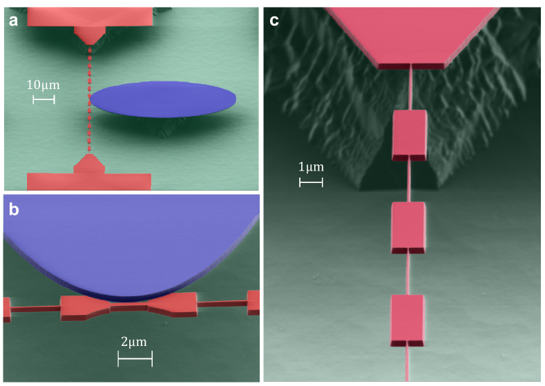
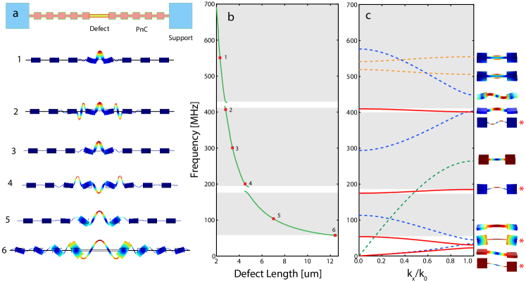
We first consider the device shown in Fig. 1. Here a high-stress Si3N4 thin film has been patterned into a 1D PnC with a beam-like defect at its center. From the standpoint of the beam, the crystal acts like a radiation shield Yu et al. (2014); Tsaturyan et al. (2014); Chan et al. (2012), the performance of which is determined by the band structure of the box-shaped unit cell. A simulation of the dispersion diagram of the unit cell is shown in Fig. 2c, with lines of different color corresponding to modes of the cell with different symmetries. In this work, we consider only in-plane flexural modes because of their compatibility with displacement readout (using the microcavity-based sensor shown in blue in Fig. 1). Pseudo-bandgaps for in-plane symmetry are indicated by gray shading in Fig. 2c. The presence of a bandgap implies strong reflection of waves from the PnC. It also implies the support of localized defect modes. To illustrate this concept, a simulation of the fundamental flexural mode of a beam embedded in a 14-element PnC is shown in Fig. 2b. Dimensions of the beam and unit cell are given in the caption. The beam’s length is varied to span the frequency range of the three bandgaps shown in Fig. 2c. Qualitatively, it is evident that modes which are well-centered in a bandgap (1,3,5) exhibit strong confinement. Conversely, modes near the edge of a bandgap (2,4,6) penetrate deeply into the PnC. This is because the defect modes start to hybridize with the in-plane modes of the unit cell, shown as red curves in Fig. 2c.
Our central claim is that localized defect modes will exhibit reduced radiation loss and similar effective mass relative to unshielded beams. To demonstrate this concept, shielded and unshielded beams of various lengths were fabricated (see sup ) and tested. To probe mechanical displacement, an elliptical microdisk cavity is patterned next to each beam, separated by nm. Whispering gallery modes of the microdisk are excited with a detuned 1550 nm laser field using a tapered optical fiber, enabling evanescent displacement readout Anetsberger et al. (2009) with an imprecision of 1 fm. All measurements were performed in a vacuum chamber at mbar in order to reduce gas damping. In conjunction with the relatively large cavity linewidth of GHz (mitigating radiation pressure effects), this enables non-invasive thermal noise measurements for beams as short as 4 m.
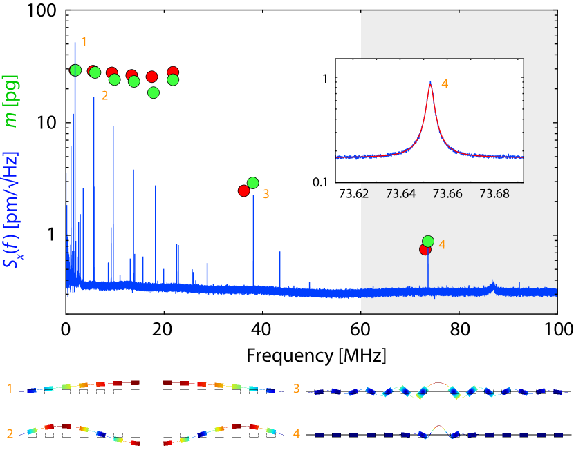
As a demonstration of spatial mode confinement, the thermal displacement noise spectrum of a 5 m-long defect embedded in a 100 m-long, 14-cell PnC is presented in Fig. 3. The fundamental in-plane mode of the defect appears at 74 MHz, situated within a large, spectrally quiet window coinciding with the pseudo-bandgap of the PnC. The small effective mass of the defect mode manifests in the relatively large area beneath the thermal noise peak . Comparing for the defect mode to that of adjacent peaks (green points) reveals a 1000-fold decrease in relative to the fundamental in-plane mode of the extended structure. Quantitative agreement of this scaling with an FEM simulation (red points, assuming a point-like probed at the midpoint of the defect) corroborates an estimated effective mass of pg for the localized mode. The corresponding fitted mechanical linewidth is kHz (), giving access to a low thermal-noise-limited force sensitivity of .
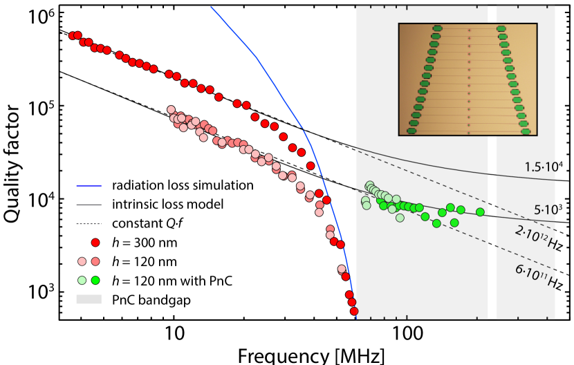
To assess the performance of the PnC as an acoustic shield, we have made a comprehensive study of vs for shielded and unshielded beams of various lengths, using thermal noise measurements as in Fig. 3. Results are compiled in Fig. 4. Green and red points correspond to shielded and unshielded beams with lengths of m and m, respectively, comprising a total of 121 independent devices. The most striking feature is a sharp transition at MHz, corresponding to m, at which the of unshielded beams changes from to a . By contrast, shielded beams with m exhibit a roughly constant , suggesting a qualitatively different loss mechanism compared to unshielded beams.
To understand the scaling of in Fig. 4, we consider a model of the form , where and are models of loss due to internal friction and radiation of acoustic waves (phonon tunneling Wilson-Rae (2008)) into the solid-state supports, respectively. We first consider internal loss, adopting a standard model that treats the film as an anelastic plate subject to cyclic loading González and Saulson (1994); Yu et al. (2012); Schmid et al. (2011); Villanueva and Schmid (2014); Unterreithmeier et al. (2010). In this approach, friction is treated as a delay between internal strain and stress (i.e., a complex Young’s modulus, ) Zener (1938). The enhanced of stressed films is related to a renormalization of the total elastic energy, viz., adding tensile stress contributes an energy due to elongation, , without substantially increasing the energy stored in bending, (which gives rise to dissipation) Unterreithmeier et al. (2010). The of a stressed film is thus enhanced relative to the unstressed case by approximately . The magnitude of the ‘loss-dilution’ factor depends on the stressed mode shape. For the string-like modes of stressed beams with thickness , it can be shown that Yu et al. (2012); Villanueva and Schmid (2014); Unterreithmeier et al. (2010)
| (1) |
where . Underbrackets here indicate contributions due to bending at the clamping points and at the antinodes of the flexural mode, respectively, which depends on the mode order, . The value of can be estimated from the dispersion relation
| (2) |
where .
Eq. (1) and Eq. (2) are used to model the internal loss of beams with two widths ( nm) in Fig. 4 (solid black lines). A value of is obtained by fitting measurements of versus to Eq. (2) (see Fig. 5). A value of is obtained by bootstrapping to the scaling of long () unshielded beams. The inferred surface loss coefficient of agrees well with the findings of Villanueva et. al. Villanueva and Schmid (2014); however, cannot be accessed directly with unshielded beams due the large deviation from the internal loss model for MHz ). Remarkably, the of shielded beams (green points) recovers to the expected internal loss scaling for MHz ), suggesting that the loss mechanism is acoustic radiation.
To confirm that the deviation from the internal loss model in Fig. 4 is due to acoustic radiation, we have conducted a no-free-parameter finite element simulation using COMSOL (for details see sup ). The geometry and stress-profile of the beam and PnC are determined from SEM imaging. The result of the simulation is shown as a solid blue line Fig. 4 and agrees qualitatively well with the data. Notably, the cutoff frequency for radiation losses depends sensitively son the geometry of the beam near the end-supports, as well as the support pillars (also included in the model). Chamfering the beam at its ends, as shown in Fig. 1 reduces the knee to MHz, which is lower than has been observed for beams of similar dimensions with no end-chamfer Huang et al. (2005).
Having addressed the challenge of reducing radiation loss in short, VHF beams, we now study a strategy for achieving high while keeping fixed, by using higher order modes. Assuming and treating as a continuous variable in Eq. (1) and Eq. (2), the maximum is obtained at and is given by
| (3) |
Therefore high may be obtained by using high order modes of long and thin beams. We note that demonstrations of high-stress Si3N4 membranes with Hz also exploit this scaling, with the mode index in Eq. (1) and Eq. (2) replaced by . For diagonal modes (), this results in an increase of Eq. (3) by a factor of . Interestingly, the conventionally higher reported for membranes as compared to nanobeams appears to be related to the fact that larger membranes ( mm) have been studied Wilson et al. (2009); Yu et al. (2012); Chakram et al. (2014).
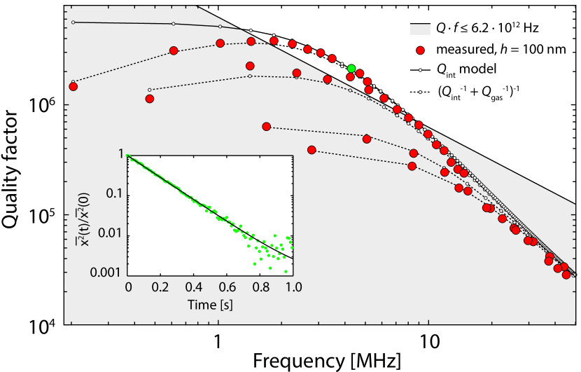
To explore the prediction made in Eq. (3), we have measured and for odd-ordered modes of unshielded beams with thickness nm and lengths varying from mm. Results are shown in 5. To mitigate systematic error associated with the sub-Hz mechanical linewidths, in this case was extracted from ringdown measurements. To perform a ringdown, the beam is resonantly excited using a piezo located beneath the sample chip; the drive is then shuttered off while displacement is continuously recorded using a network analyzer (with bandwidth ). For the longest beam, , we observe a maximum of for . We compare this to a model curve for (solid black line) based on a value of estimated by fitting the dispersion relation (Eq. (2)). The model predicts to within , but qualitatively overestimates for lower frequencies. This discrepancy is due to gas damping, which contributes a systematic additional damping of Hz.
We emphasize that while the concept of PnC acoustic shielding has recently been explored in the context of nanomembranes Yu et al. (2014); Tsaturyan et al. (2014) and nanobeams Chan et al. (2012), our results, to the best of the authors’ knowledge, represent the first explicit demonstration that the intrinsic of a nanomechanical resonator can be recovered in the presence of otherwise dominant radiation loss. Moreover, the value of demonstrated in Fig. 5 establishes a new benchmark for high-stress SiN nanobeams. In conjunction with the large zero-point motion and sparse mode density of nanobeams, and building on recent advances in near-field cavity optomechanical coupling Wilson et al. (2015); Schilling et al. (2016), we envision application of these dissipation engineering strategies towards a new generation of quantum optomechanics experiments based on Heisenberg-limited measurements Wilson et al. (2015), perhaps even at room temperature. Nanoscale PnCs are furthermore readily extended to alternative materials such as diamond Khanaliloo et al. (2015), opening the door for studying the microphysics of internal loss Groeblacher et al. (2015). PnC-shielded nanoresonators may also find application as high frequency mechanical filters and oscillators Teva et al. (2008); Feng et al. (2008).
The authors thank Dr. Michael Zervas and Dr. Zdenek Benes for fabrication advice. All samples were fabricated at the CMi (Center of MicroNanotechnology) at EPFL. Research was carried out with support from an ERC Advanced Grant (QuREM), from the Swiss National Science Foundation and through grants from the NCCR of Quantum Engineering (QSIT). D.J.W. acknowledges support from the European Commission through a Marie Skłodowska-Curie Fellowship (IIF project 331985).
References
- Imboden and Mohanty (2014) M. Imboden and P. Mohanty, Phys. Rep. 534, 89 (2014).
- Zwickl et al. (2008) B. M. Zwickl, W. E. Shanks, A. M. Jayich, C. Yang, A. C. Bleszynski Jayich, J. D. Thompson, and J. G. E. Harris, Appl. Phys. Lett. 92, 103125 (2008).
- Wilson et al. (2009) D. Wilson, C. Regal, S. Papp, and H. Kimble, Phys. Rev. Lett. 103, 207204 (2009).
- Thompson et al. (2008) J. D. Thompson, B. M. Zwickl, A. M. Jayich, F. Marquardt, S. M. Girvin, and J. G. E. Harris, Nature 452, 72 (2008).
- Purdy et al. (2013) T. P. Purdy, R. W. Peterson, and C. A. Regal, Science 339, 801 (2013).
- Unterreithmeier et al. (2010) Q. P. Unterreithmeier, T. Faust, and J. P. Kotthaus, Phys. Rev. Lett. 105, 027205 (2010).
- Schmid et al. (2011) S. Schmid, K. D. Jensen, K. H. Nielsen, and A. Boisen, Phys. Rev. B 84, 165307 (2011).
- Yu et al. (2012) P.-L. Yu, T. Purdy, and C. Regal, Phys. Rev. Lett. 108, 083603 (2012).
- Villanueva and Schmid (2014) L. G. Villanueva and S. Schmid, Phys. Rev. Lett. 113, 227201 (2014).
- González and Saulson (1994) G. I. González and P. R. Saulson, J. Acoust. Soc. Am. 96, 207 (1994).
- Chakram et al. (2014) S. Chakram, Y. S. Patil, L. Chang, and M. Vengalattore, Phys. Rev. Lett. 112, 127201 (2014).
- Norte et al. (2015) R. A. Norte, J. P. Moura, and S. Gröblacher, arXiv preprint arXiv:1511.06235 (2015).
- Tsaturyan et al. (2014) Y. Tsaturyan, A. Barg, A. Simonsen, L. G. Villanueva, S. Schmid, A. Schliesser, and E. S. Polzik, Opt. Exp. 22, 6810 (2014).
- Yu et al. (2014) P.-L. Yu, K. Cicak, N. Kampel, Y. Tsaturyan, T. Purdy, R. Simmonds, and C. Regal, App. Phys. Lett. 104, 023510 (2014).
- Anetsberger et al. (2009) G. Anetsberger, O. Arcizet, Q. P. Unterreithmeier, R. Rivière, A. Schliesser, E. M. Weig, J. P. Kotthaus, and T. J. Kippenberg, Nat. Phys. 5, 909 (2009).
- Jensen et al. (2008) K. Jensen, K. Kim, and A. Zettl, Nat. Nano. 3, 533 (2008).
- Cleland and Roukes (1998) A. N. Cleland and M. L. Roukes, Nature 392, 160 (1998).
- Mamin and Rugar (2001) H. Mamin and D. Rugar, App. Phys. Lett. 79, 3358 (2001).
- Wilson et al. (2015) D. Wilson, V. Sudhir, N. Piro, R. Schilling, A. Ghadimi, and T. Kippenberg, Nature 524, 325 (2015).
- Huang et al. (2005) X. Huang, X. Feng, C. Zorman, M. Mehregany, and M. Roukes, New J. Phys. 7 (2005).
- Goettler et al. (2010) D. Goettler, M. Su, Z. Leseman, Y. Soliman, R. Olsson, and I. El-Kady, J. App. Phys. 108, 084505 (2010).
- Mohammadi et al. (2011) S. Mohammadi, A. A. Eftekhar, R. Pourabolghasem, and A. Adibi, Sens. Act. A: Phys. 167, 524 (2011).
- Hsu et al. (2011) F.-C. Hsu, J.-C. Hsu, T.-C. Huang, C.-H. Wang, and P. Chang, App. Phys. Lett. 98, 143505 (2011).
- Chan et al. (2012) J. Chan, A. H. Safavi-Naeini, J. T. Hill, S. Meenehan, and O. Painter, App. Phys. Lett. 101, 081115 (2012).
- (25) Supplementary Information .
- Zener (1938) C. Zener, Phys. Rev. 53, 90 (1938).
- Schilling et al. (2016) R. Schilling, H. Schütz, A. Ghadimi, V. Sudhir, D. J. Wilson, and T. J. Kippenberg, arXiv preprint arXiv:1601.06745 (2016).
- Khanaliloo et al. (2015) B. Khanaliloo, H. Jayakumar, A. C. Hryciw, D. P. Lake, H. Kaviani, and P. E. Barclay, arXiv:1502.01788 (2015).
- Groeblacher et al. (2015) S. Groeblacher, A. Trubarov, N. Prigge, G. D. Cole, M. Aspelmeyer, and J. Eisert, Nat. Comm. 6, 7606 (2015).
- Teva et al. (2008) J. Teva, A. G. Berini, A. Uranga, J. Verd, F. Torres, J. Lopez, J. Esteve, F. Pérez-Murano, and N. Barniol, Proc. IEEE MEMS 2008 (2008).
- Feng et al. (2008) X. Feng, C. White, A. Hajimiri, and M. L. Roukes, Nat. Nano. 3, 342 (2008).
Supplementary information for
“Dissipation engineering of high-stress silicon nitride nanobeams”
I I. Sample fabrication
I.1 A. Overview
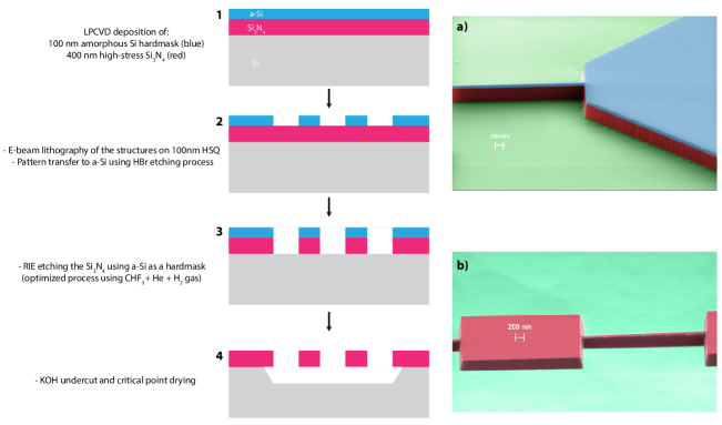
Nanobeam-microdisk samples as shown in Fig. 1 of the main text are fabricated according to the procedure outlined in Fig. 1. The process begins with a series of low pressure chemical vapor deposition (LPCVD) steps on a 4” CZ Si wafer. 400 nm of stoichiometric Si3N4 (SiN) is deposited at 800∘C, followed by 100 nm of amorphous Si (a-Si) at 500∘C (to be used as a hard mask). The microdisk and nanobeam are patterned on top of the a-Si film by electron beam lithography, in 100 nm of HSQ. The pattern is transfered into the a-Si film (creating a hard mask for the subsequent SiN etch) using a HBr etch process. The pattern is then transfered into the SiN film by reactive ion etching, using an SPTS APS Dielectric Etcher and CHF3 chemistry. The process is concluded by undercutting the microdisk and nanobeam with KOH, followed by critical point drying.
I.2 B. Fabrication considerations related optomechanical coupling
The fabrication process was developed and optimized with two goals in mind: (1) to minimize the in-plane gap () between the nanobeam and the microdisk and (2) to minimize the sidewall roughness of the microdisk. Small is desirable as it gives rise to a large parametric (optomechanical) coupling between the lateral position of the beam and the frequency of the microdisk whispering gallery mode (WGM) Aspelmeyer et al. (2014). For beams with in-plane thickness much smaller than the operating wavelength , it can be shown that , where is the in-plane evanescent decay length of the WGM Anetsberger et al. (2009). Thus a design gap of nm was chosen in conjunction with an operating wavelength of nm. Low sidewall roughness is desirable in order to reduce the possibility of WGM loss () due to Rayleigh scattering from the disk’s surface Borselli et al. (2004). Collectively, increasing and reducing was crucial to achieving the high sensitivity displacement measurements shown in Fig. 3 and employed in Figs. 4-5 of the main text. For example, in Fig. 3 of the main text, the thermomechanical signal-to-noise (in this case dominated by electronic detector noise) is proportional to , where is the optical input power Aspelmeyer et al. (2014).
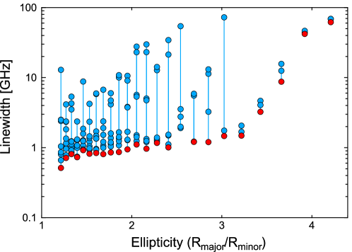
The requirements for etching optically smooth sidewalls separated by nm depends on the thickness of the SiN film. We chose a nm-thick film as a compromise between achieving a large WGM evanescence and low WGM radiation loss. Achieving a vertical nm gap thus required etching SiN with an aspect ratio much better than 1:4. We found that achieving this aspect ratio while maintaining an optically smooth surface was difficult with standard RIE etching techniques (employing standard e-beam resists), due to mask erosion. It is for this reason that a-Si was employed as a secondary hard mask. a-Si provides high selectivity (1:10) relative to SiN in RIE as well as high resistance to mask erosion. Thus we have achieved gaps as small as nm and relatively smooth sidewalls, characterized by optical quality factors in excess of in the absence of a beam (see Fig. 2). For the results shown in Figs. 3-5 of the main text, we employed elliptical microdisks with a fixed circumference of approximately m, an ellipticity (major radius over minor radius) ranging from 1 to 4, and nm. Typical intrinsic optical linewidths of GHz were observed. An estimate of MHz/nm is obtained by approximating the microdisk WGM profile with the analytical form of a microtoroid WGM, as discussed in Anetsberger et al. (2009); Schilling et al. (2016).
II II. Acoustic radiation loss model
II.1 A. Overview
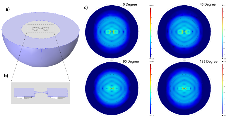
The radiation loss model shown in Fig. 4 of the main text was obtained by computing the complex eigenfrequency spectrum of the mechanical structure surrounded by numerically implemented PML (perfectly matched layer, corresponding to a perfectly impedance matched and aborbing boundary). We used the COMSOL Structural Mechanics Finite Element Analysis software package for this simulation. The modeled structure is shown in gray in Fig. 2a, and includes the SiN defect beam, SiN PnC, SiN support pads, the Si pillars beneath each support pad, a half-spherical section of the Si substrate. The blue shell in Fig. 2a corresponds to the PML. By placing the PML far from the nanobeam, we ensure that reflection of acoustic waves from the supports is accounted for in the simulation. We also ensure that the size of the PML is large enough that its own reflection coefficient is negligible Wilson-Rae (2008); Wilson-Rae et al. (2011). Visualization of acoustic radiation into the PML is shown in Fig. 2c. Radiation loss manifests as an imaginary component of each numerically computed eigenfrequency, . The eigenfrequency of the defect mode is identified based on its mode shape. Radiation-loss-limited -factors (blue curve in Fig. 4 of the main text) are obtained from the formula:
| (1) |
The location of the knee point in the model of versus in Fig. 4 of the main text depends on the dimensions of the extended mechanical structure, in particular that of Si pillars and the trapezoidal end-points of the beam (c.f. Fig. 1a in the main text). The blue curve shown in Fig. 4 of the main text employs dimensions obtained from SEM imaging and uses no fit parameters.
II.2 B. Role of number of unit cells
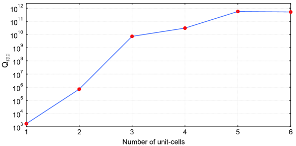
The acoustic impedance of the PnC depends on the number of unit cells used. We employed a 7-cell PnC to obtain the results described in the main text. This choice was based on a model of versus number of cells. An example is shown in Fig. 4: here a 2.3 m defect with a frequency of 542 MHz is embedded in the 3rd bandgap of the PnC described in Fig. 2 of the main text. As illustrated in the figure, only 3 cells are required to reduce the radiation loss by a factor of , to a value orders of magnitude larger than ; also shielding evidently saturates at cells. A conservative choice of 7 cells was made in the experiment to allow for design imperfections.
References
- Aspelmeyer et al. (2014) M. Aspelmeyer, T. J. Kippenberg, and F. Marquardt, Rev. Mod. Phys. 86, 1391 (2014).
- Anetsberger et al. (2009) G. Anetsberger, O. Arcizet, Q. P. Unterreithmeier, R. Riviére, A. Schliesser, E. M. Weig, J. P. Kotthaus, and T. J. Kippenberg, Nat. Phys. 5, 909 (2009).
- Borselli et al. (2004) M. Borselli, K. Srinivasan, P. E. Barclay, and O. Painter, App. Phys. Lett. 85, 3693 (2004).
- Schilling et al. (2016) R. Schilling, H. Schütz, A. Ghadimi, V. Sudhir, D. J. Wilson, and T. J. Kippenberg, arXiv preprint arXiv:1601.06745 (2016).
- Wilson-Rae (2008) I. Wilson-Rae, Phys. Rev. B 77, 245418 (2008).
- Wilson-Rae et al. (2011) I. Wilson-Rae, R. Barton, S. Verbridge, D. Southworth, B. Ilic, H. Craighead, and J. Parpia, Phys. Rev. Lett. 106, 047205 (2011).