Size quantization of Dirac fermions in graphene constrictions
Quantum point contacts (QPCs) are cornerstones of mesoscopic physics and central building blocks for quantum electronics. Although the Fermi wavelength in high-quality bulk graphene can be tuned up to hundreds of nanometers, the observation of quantum confinement of Dirac electrons in nanostructured graphene systems has proven surprisingly challenging. Here we show ballistic transport and quantized conductance of size-confined Dirac fermions in lithographically-defined graphene constrictions. At high charge carrier densities, the observed conductance agrees excellently with the Landauer theory of ballistic transport without any adjustable parameter. Experimental data and simulations for the evolution of the conductance with magnetic field unambiguously confirm the identification of size quantization in the constriction. Close to the charge neutrality point, bias voltage spectroscopy reveals a renormalized Fermi velocity ( m/s) in our graphene constrictions. Moreover, at low carrier density transport measurements allow probing the density of localized states at edges, thus offering a unique handle on edge physics in graphene devices.
The observation of unique transport phenomena in graphene, such as Klein tunneling You09 , evanescent wave transport Two06 , or the half-integer Nov05 ; Zha05 and fractional Du09 ; Bol09 quantum Hall effect are directly related to the material quality as well as the relativistic dispersion of the charge carriers. As the quality of bulk graphene has been impressively improved in the last years Dean10 ; Wan13 , the understanding of the role and limitations of edges on transport properties of graphene is becoming increasingly important. This is particularly true for nanoscale graphene systems where edges can dominate device properties. Indeed, the rough edges of graphene nanodevices are most probably responsible for the difficulties in observing clear confinement induced quantization effects, such as quantized conductance Lin08 and shell filling wang11 . So far signatures of quantized conductance have only been observed in suspended graphene, however with limited control and information on geometry and constriction width Tom11 . More generally, with further progress in fabrication technology, graphene nanoribbons and constrictions are expected to evolve from a disorder dominated Sarma11 ; Ter11 ; Danneau08 ; Borunda13 transport behavior to a quasi-ballistic regime where boundary effects, crystal alignment, and edge defects Mas12 ; Baringhaus14 govern the transport characteristics. This will open the door to investigate interesting phenomena arising from edge states, including magnetic order at zig-zag edges Magda14 , an unusual Josephson effect, unconventional edge states Plotnik14 , magnetic edge-state excitons Yang08 or topologically protected quantum spin Hall statesYoung14 .
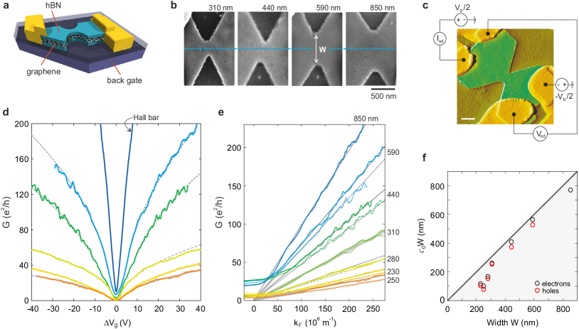

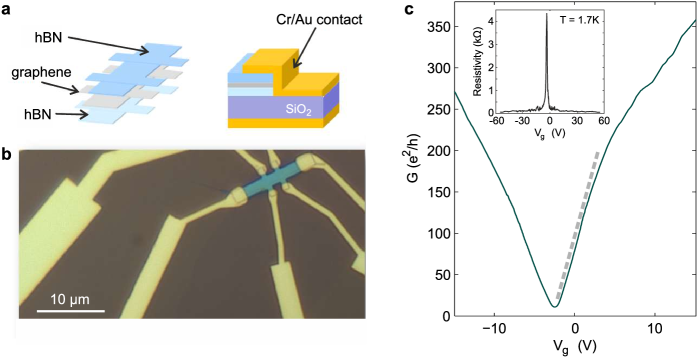
In this work we report on the observation of quantum confinement and edge states in ballistic transport through graphene constrictions approximating quantum point contacts. We prepared 4-probe devices based on high-mobility graphene-hexagonal boron nitride (hBN) sandwiches on SiO2/Si substrates and use reactive ion etching to pattern narrow constrictions (see Methods) with widths ranging from 230 to 850 nm, connecting wide leads (Figs. 1a-1c). The graphene leads are side-contacted Wan13 by chrome/gold electrodes. A back gate voltage is applied on the highly doped Si substrate to tune the carrier density in the graphene layer, , where is the so-called lever arm and is the gate voltage of the minimum conductance, i.e. the charge neutrality point. To demonstrate the high electronic quality of our graphene-hBN sandwich structures we show the gate characteristic of a reference Hall bar device (Fig. 1d). From this data we extract a carrier mobility in the range of around 150.000 cm2/Vs (see Supplementary Note 1), resulting in a mean free path exceeding 1 m at around V. Thus, the mean free path is expected to clearly exceed all relevant length scales in our constriction devices giving rise to ballistic transport.
Results
Ballistic transport.
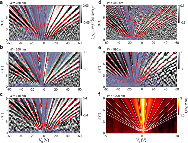
We measure the conductance as function of gate voltage for a number of constrictions with different widths (Fig. 1d; see labels in Fig. 1e). The observed square root dependence (see dashed lines in Fig. 1d) is a first indication of highly ballistic transport in our devices. Indeed, according to the Landauer theory for ballistic transport, the conductance through a perfect constriction increases by an additional conductance quantum whenever reaches a multiple of ,
| (1) |
where is the Fermi wave number, the factor four accounts for the valley and spin degeneracies, is the step function, and we have neglected minor phase contributions due to details of the graphene edgeOstaay11 for simplicity. Fourier expansion of Eq. (1) yields
| (2) |
For an ideal constriction = 1, , and , . In the presence of edge roughness, is reduced to a value below 1 due to limited average transmission, and higher Fourier components are expected to decay in magnitude and acquire random scattering phases . Consequently, the sharp quantization steps turn into periodic modulations as will be shown below. Averaged over these modulations only the zeroth order term in the expansion [Eq. (2)] survives. This mean conductance of a constriction of width thus features a linear dependence on , or, equivalently, a square-root dependence as a function of back-gate voltage assuming an energy-independent transmission of all modes, in accord with Fig. 1d. By measuring the carrier density dependent quantum Hall effect at high magnetic fieldsYZhang05 ; Novoselov07 , we can independently determine the gate coupling for each device (see Supplementary Note 2). We can thus unfold the dependence on and study both the electron and hole conductance as function of (Fig. 1e). From the linear slopes of , the product can be extracted for each device and compared to its width (Fig. 1f) determined from scanning electron microscopy (SEM) images (see, e.g., Fig. 1b). The estimates for extracted from lie just little below the width , where decreases for decreasing width. This suggests that for the narrower devices reflections, most likely due to device geometry and edge roughness, are playing a more important role. From the data in Fig. 1f we can extract for our smallest constriction. Below we will show that, indeed, reflections at the rough edges of the constriction and not a reduction in active channel width is responsible for the deviation of the experimentally extracted from the SEM width .
Localized states at the edges.
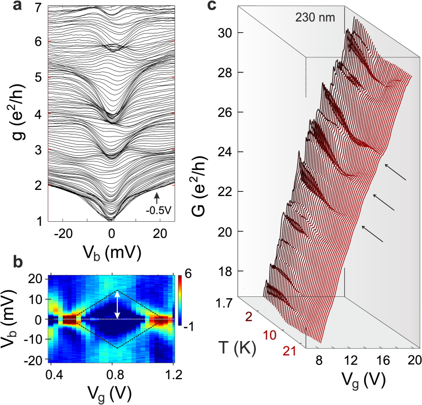
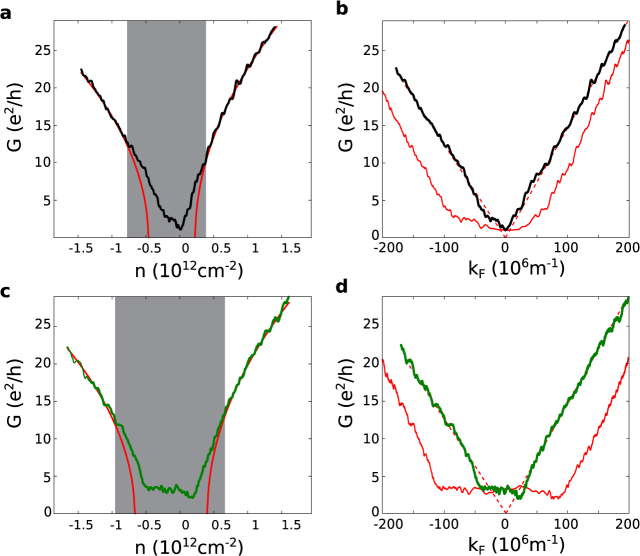
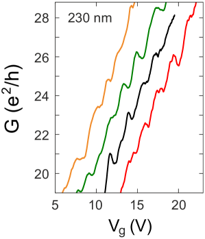
For small m-1 (i.e. low carrier concentrations) the measured conductances systematically deviate from the expected linear behavior (see Fig. 1e). This deviation from the square-root relation between and (i.e. ) becomes more apparent when focusing on around the charge neutrality point (CNP). The conductance as function of for two different cool-downs of the same graphene constriction ( 230 nm, Fig. 2a), shows marked cool-down dependent low carrier density regions with substantial deviations from . Far away from the CNP, the conductance as function of for both cool-downs shows (i) an identical behavior leading to the very same and (ii) almost identical, regularly spaced kink structures (see arrows in Fig. 2a), which are, however, slightly shifted relative to another on the carrier density axis . These observations suggest that the square-root relation between the Fermi wave vector and the gate voltage , i.e. needs to be modified. While the quantum capacitance of ideal graphene can be neglected Ilani06 ; Fang07 ; Reiter14 , a small additional contribution from, e.g., localized trap states modifies the relation between and to
| (3) |
Far away from the Dirac point (), we recover the expected square root relation. Close to the Dirac point, however, will be strongly modified by deviations from the linear density of states of ideal Dirac fermions and approaches near the CNP.
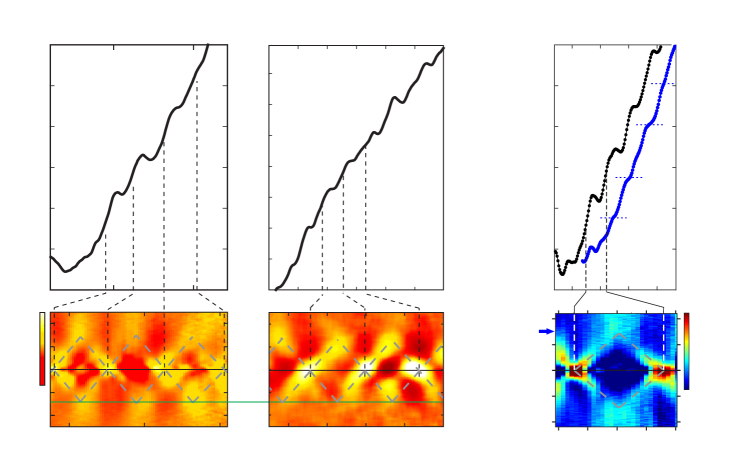
The trap states do not contribute to transport, yet they contribute to the charging characteristics Bischoff14 . It is important to note that electron-hole puddles LeRoySTM or charged impurities would only smear out the density of states but would not add additional trap-state density . This is in contrast to graphene edges, in particular rough graphene edges, which feature a significant number of trap states. For example, a tight-binding simulation of the local density of states of the experimental geometry yields a strong clustering of localized states at the device edges (see Fig. 2c), which energetically lie close to the CNP (Fig. 2e). The deviation of from the scaling also opens up the opportunity to extract from experimental conductance data (e.g. Fig. 2d), and thus a new pathway for device characterization. Inspired by the tight-binding simulation, we approximate the trap state density as function of Fermi wave vector by a Gaussian distribution. We fit the position, height and width of the Gaussian by minimizing the difference between the measured and the corresponding linear extrapolation to very low values of (see Fig. 2b and Supplementary Note 3). We find good qualitative agreement between simulation and experiment (compare Figs. 2d and 2e). Quantitative correspondence would require a detailed, microscopic model for the trap state density . Note that the only difference between different traces in Figs. 2a, 2b and 2d is the exposition of the device to air for several days leading to a wider carrier density region of substantial deviations (green trace). The number of trap states (i.e., the deviations around the CNP) is significantly enhanced (compare also green and black trace in Fig. 2d). As the active graphene layer is completely sandwiched in hBN only the graphene edges are exposed to air and, very likely, experience chemical modifications. In line with our numerical results, we thus conjecture that localized states at the edges substantially contribute to , leading to the strong cool-down dependence we observe in our measurements. While this interpretation seems plausible and is consistent with our data, alternative explanations cannot be ruled out.
Away from the CNP our data agrees remarkably well with ballistic transport simulations through the device geometry using a modular Green’s function approach LibischNJP (see blue trace in Fig. 2b): we simulate the 4-probe constriction geometry taken from a SEM image, scaled down by a factor of four to obtain a numerically feasible problem size liu15 . To account for the etched edges in the devices, we include an edge roughness amplitude of for the constriction. This comparatively large edge roughness (which is consistent with the systematic reduction of transmission through the constriction when using the average conductance) is probably due to microcracks at the edges of the device.
Quantized conductance.
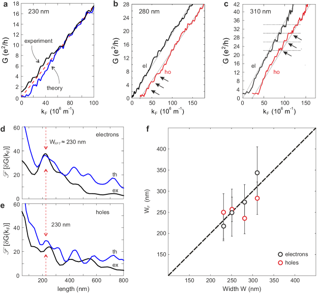
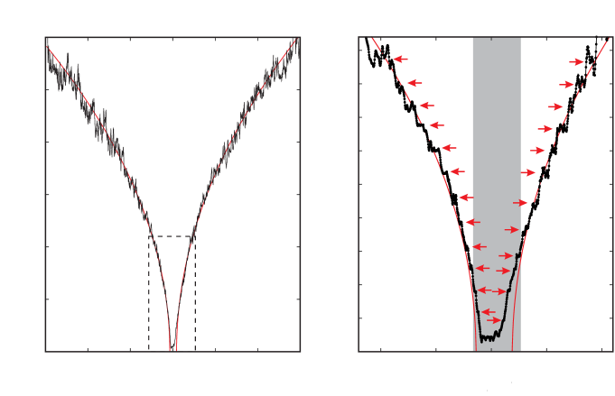
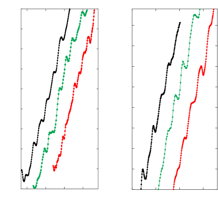
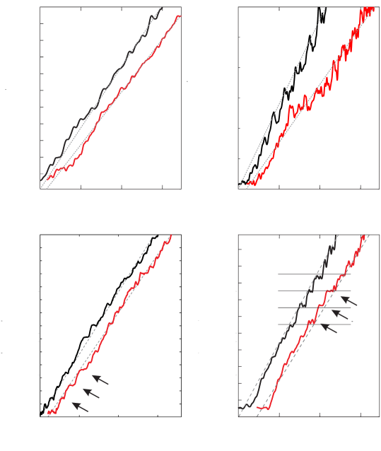
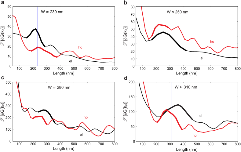
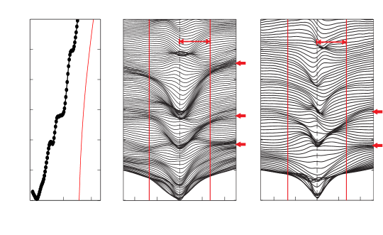
Superimposed on the overall linear behavior of , we find reproducible modulations (“kinks”) in the conductance (see Figs. 3a-3c and Fig. S4b). The kinks are well reproduced for several cool downs (see arrows in Fig. 2a and Supplementary Note 4) as well as for different devices, generally showing a spacing varying in the range of (see arrows in Figs. 3b and 3c). The “step height” and its sharpness depend on the carrier density (i.e. ) as well as on the constriction width and is strongly influenced by the overall transmission (Fig. 1f). Remarkably, we observe a spacing of the steps close to for one of our wide samples ( 310 nm) at elevated conductance values on both the electron and hole sides (see arrows and horizontal lines in Fig. 3c and Fig. S4b)
Our assignment of the conductance “kinks” as signatures of quantized flow through the constriction is supported by our theoretical results. Theory and experimental data from the smallest constriction show similar smoothed, irregular modulations (see Fig. 3a), instead of sharp size quantization steps.Per06 The replacement of sharp quantization steps by kinks reflects the strong scattering at the rough edges of the device Muc09 ; Ihnatsenka12 , resulting in the accumulation of random phases in the Fourier components of [Eq. (2)]. We note that calculations with smaller edge disorder show a larger average conductance, yet very similar “kink” structures. As the present calculation includes only edge-disorder induced scattering while neglecting other scattering channels such as electron-electron or electron-phonon scattering, the good agreement with the data suggests edge scattering to be the dominant contribution to the formation of the “kinks”. By contrast, both experimental and theoretical investigations of, e.g., semiconducting GaAs heterostructures show very clear, pronounced quantization plateausvanWeesConductance . In these heterostructures, the electron wave length near the point is very long, and cannot resolve edge disorder on the nanometer scale. By contrast, - scattering in graphene allows conduction electrons to probe disorder on a much shorter length scale. Consequently, edge roughness substantially impacts transport. The comparison between experimental and theoretical data (Fig. 3a) unambiguously establishes the observed modulations to be consistent with the smoothed size quantization effects predicted by theory.
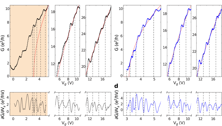
By subtracting the zeroth-order Fourier component (or ), the superimposed modulations of the conductance provide direct information on the quantized conductance through the constriction [Eq. (2)]. One key observation is that the Fourier transform of offers an alternative route towards the determination of the constriction width complementary to that from the mean conductance . For example, the pronounced peak of the first harmonic at nm (red arrows in Figs. 3d and 3e) is consistent with the constriction width derived from the SEM image. Interestingly, our simulation also correctly reproduces the experimental observation that the peak in the Fourier spectrum of is more pronounced on the electron side (Fig. 3d) than on the hole side. This results from the slightly asymmetric energy distribution of the trap states relative to the CNP, which is accounted for in our tight-binding calculation.
Performing such a Fourier analysis for several devices (Supplementary Note 5) yields much closer agreement with the geometric width (Fig. 3f and horizontal axis of Fig. 1f) than an estimate based only on the zeroth-order Fourier component [first term in Eq. (2), see vertical axis of Fig. 1f]. Fourier spectroscopy of conductance modulations thus allows to disentangle reduced transmission due to scattering at the edges () from the effective width of the constriction, and proves the relation between the observed Fourier periodicity and the device geometry.
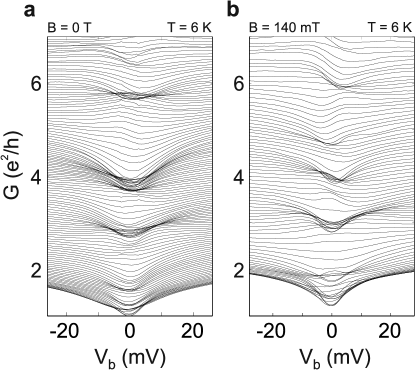
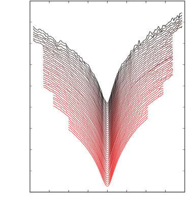
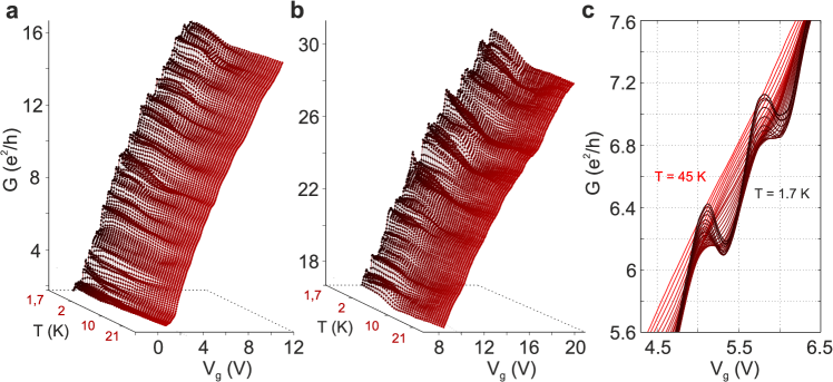
Bias voltage spectroscopy measurements yield an estimate for the energy scale of the size quantization steps Tom11 ; wep13 . For example, by analyzing finite bias measurements from our smallest constriction device we extract a subband energy spacing of 13.5 2 meV near the CNP (Figs. 4a, 4b and Supplementary Note 6). With the geometric width of 230 nm also confirmed by the Fourier spectroscopy (Fig. 3c) we can estimate the Fermi velocity near the CNP as m/s. This is a clear signature of a substantially renormalized Fermi velocity in nanostructured graphene, possibly enhanced by electron-electron interaction Elias11 . Moreover, the extracted energy scales are consistent with the weak temperature dependence of the quantized conductance (Fig. 4c and Supplementary Note 7).
Transition from quantized conductance to quantum Hall.
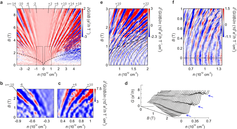
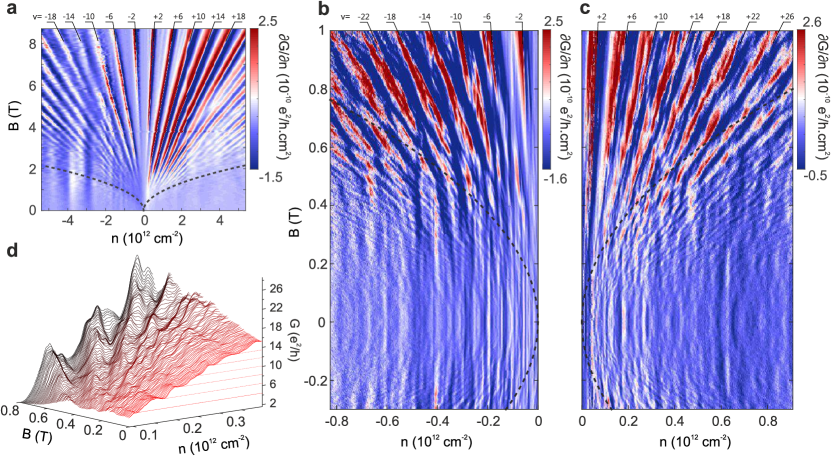
Additional clear fingerprints of size quantization appear in the parametric evolution of the conductance steps gui12 with magnetic field, . The transition from size quantization at zero -field to Landau quantization at high magnetic fields occurs when the cyclotron radius becomes smaller than half the constriction width . For the Landau level the transition should occur at with the magnetic length. This transition line in the plane (see black dashed curve in Fig. 5a) agrees well with the onset of Landau level formation in our data (see Supplementary Note 8 for similar data from a 280 nm constriction device). The evolution of the lowest quantized steps (at = 0 T) to the corresponding lowest Landau levels at low temperatures (T=1.7 K) can be easily tracked (see Figs. 5b and 5c). At higher temperatures ( K) the evolution of quantized sub-bands to Landau levels is observed even for higher conductance plateaus (Fig. 5d, 5e). For a comparison, we calculate the evolution of size quantization of an infinitely long ribbon of width as function of magnetic field. We take nm from the SEM data, which leaves no adjustable parameters. Our model ( black lines in Figs. 5e and 5f) reproduces the evolution from the kinks at small fields () to the Landau levels for large fields () remarkably well, further supporting the notion that they are, indeed, signature of size quantization.
Discussion
We have shown ballistic conductance of confined Dirac fermions in high-mobility graphene nanoconstrictions sandwiched by hexagonal boron nitride. Away from the Dirac point, we observe a linear increase in conductance as function of Fermi wavevector with a slope proportional to constriction width. Close to the Dirac point, the charging of localized edge states distorts this linear relation. Superimposed on the linear conductance, we observe reproducible, evenly spaced modulations (“kinks”). Tight-binding simulations for the device reproduce these structures related to size quantization at the constriction. We can unambiguously identify these “kinks” as size quantization signatures by both Fourier spectroscopy at zero magnetic field and their evolution with magnetic field, finding good agreement between theory and experiment.
Methods
Experimental methods and details
The hBN-graphene-hBN sandwich structures Wan13 have been etched by reactive ion etching in a atmosphere, prior deposition of a -thick Cr etching mask. Remaining rests of Cr oxide are removed by immersing the samples in a Tetramethylammonium hydroxide (TMAH) solution for about 30-35 s. All transport measurements are performed in a 4-probe configuration using standard lock-in techniques. Since the distances between the contacted current-carrying electrodes and the voltage probes are small, compared to the other length scales of the system, we have an effective 2-probe configuration. Importantly, this way we exclude the one-dimensional contact resistances.
Electrostatic simulations and transport calculations
We simulate the experimental device geometry using a third-nearest neighbor tight-binding ansatz. We rescale our device by a factor of four compared to experiment, to arrive at a numerically feasible geometry. We determine the Green’s function using the modular recursive Green’s function method Rotter06 ; LibischNJP . The local density of states and transport properties can then be extracted by suitable projections on the Green’s function. For more technical details see Supplementary Note 9.
References
- (1) Young, A.F. & Kim, P. Quantum interference and Klein tunnelling in graphene heterojunctions. Nature Phys. 5, 222 (2009).
- (2) Tworzydlo, J., et al. Sub-Poissonian Shot Noise in Graphene. Phys. Rev. Lett. 96, 246802 (2006).
- (3) Novoselov, K.S., et al. Two-dimensional gas of massless Dirac fermions in graphene. Nature 438, 197 (2005).
- (4) Zhang, Y., Tan, Y-W. Stormer, H.L. & Kim, P. Experimental observation of the quantum Hall effect and Berry’s phase in graphene. Nature 438, 201 (2005).
- (5) Du, X., Skachko, I., Duerr, F., Luican, A., & Andrei, E.Y. Fractional quantum Hall effect and insulating phase of Dirac electrons in graphene. Nature 462, 192 (2009).
- (6) Bolotin, K.I., et al. Observation of the fractional quantum Hall effect in graphene. Nature 462, 196 (2009).
- (7) Dean, C.R., et al. Boron nitride substrates for high-quality graphene electronics. Nature Nano. 5, 722 (2010).
- (8) Wang, L., et al. One-Dimensional Electrical Contact to a Two-Dimensional Material. Science 342, (6158) 614-167 (2013).
- (9) Lin, Y.M., Perebeinos, V., Chen, Z., & Avouris, P. Electrical observation of subband formation in graphene nanoribbons. Phys. Rev. B 78, 161409R (2008).
- (10) Wang, X., et al. Graphene nanoribbons with smooth edges behave as quantum wires. Nature Nanotechnology 6, 563–567 (2011).
- (11) Tombros, N., et al. Quantized conductance of a suspended graphene nanoconstriction. Nature Physics 7, 697-700 (2011).
- (12) Terrés, B., et al. Disorder induced Coulomb gaps in graphene constrictions with different aspect ratios. Appl. Phys. Lett. 98, 032109 (2011).
- (13) Das Sarma, S., Adam, S., Hwang, E.H. & Rossi, E. Electronic Transport in 2D Graphene. Rev. Mod. Phys. 83, 407 (2011).
- (14) Danneau, R. et al. Shot Noise in Ballistic Graphene. Phys. Rev. Lett. 100, 196802 (2008).
- (15) Borunda, M.F., Hennig, H. & Heller, E.J. Ballistic versus diffusive transport in graphene. Phys. Rev. B 88, 125415 (2013).
- (16) Masubuchi, S., et al. Boundary Scattering in Ballistic Graphene. Phys. Rev. Lett. 109, 036601 (2012).
- (17) Baringhaus, J., et al. Exceptional ballistic transport in epitaxial graphene nanoribbons. Nature 506, 349 (2014)
- (18) Magda, G.Z., et al. Room-temperature magnetic order on zigzag edges of narrow graphene nanoribbons. Nature 514, 608 (2014)
- (19) M. Titov & C. W. J. Beenakker Josephson effect in ballistic graphene. Phys. Rev. B. 74, 041401(R) (2006).
- (20) Plotnik, Y., et al. Observation of unconventional edge states in ‘photonic graphene’. Nature Mat. 13, 57-62 (2014)
- (21) Yang, L., Cohen, M.L. & Louie, S.G. Magnetic Edge-State Excitons in Zigzag Graphene Nanoribbons. Phys. Rev. Lett. 101, 186401 (2008).
- (22) Young, A.F., et al. Tunable symmetry breaking and helical edge transport in a graphene quantum spin Hall state. Nature 505, 528 (2014).
- (23) Van Ostaay, J.A.M., et al. Dirac boundary condition at the reconstructed zigzag edge of graphene. Phys. Rev. B 84, 195434 (2011).
- (24) Zhang, Y., Tan, Y.-W., Stormer, H.L., & Kim, P. Experimental observation of the quantum Hall effect and Berry’s phase in graphene. Nature 438, 201 (2005).
- (25) Novoselov, K.S., et al. Room-Temperature Quantum Hall Effect in Graphene. Science 315, 1379 (2007).
- (26) Reiter, R., et al. Negative quantum capacitance in graphene nanoribbons with lateral gates. Phys. Rev. B 89, 115406 (2014).
- (27) Ilani, S., et al. Measurement of the quantum capacitance of interacting electrons in carbon nanotubes. Nature Physics 2, 687 (2006).
- (28) Fang, T., et al. Carrier statistics and quantum capacitance of graphene sheets and ribbons. App. Phys. Lett. 91, 092109 (2007).
- (29) A. Deshpande, W. Bao, Z. Zhao, C. N. Lau, & B. J. LeRoy Imaging charge density fluctuations in graphene using Coulomb blockade spectroscopy Phys. Rev. B 83, 155409 (2011).
- (30) Bischoff, D., et al. Characterizing wave functions in graphene nanodevices: Electronic transport through ultrashort graphene constrictions on a boron nitride substrate. Phys. Rev. B 90, 115405 (2014).
- (31) Libisch, F., Rotter, S., & Burgdörfer, J. Coherent transport through graphene nanoribbons in the presence of edge disorder. New Journal of Physics 14, 123006 (2012).
- (32) Liu, M.-H. et al. Phys. Rev. Lett. 114, 036601 (2015).
- (33) Peres, N.M.R., et al. Conductance quantization in mesoscopic graphene. Phys. Rev. B 73, 195411 (2006).
- (34) Mucciolo, E.R., et al. Conductance quantization and transport gaps in disordered graphene ribbons. Phys. Rev. B 79, 075407 (2009).
- (35) Ihnatsenka, S. & Kirczenow, G Conductance quantization in graphene nanoconstrictions with mesoscopically smooth but atomically stepped boundaries. Phys. Rev. B 85, 121407(R) (2012).
- (36) Van Wees, B.J., et al. Quantized conductance of point contacts in a two-dimensional electron gas. Phys. Rev. Lett. 60, 848 (1988).
- (37) Van Weperen, I., et al. Quantized Conductance in an InSb Nanowire. Nano Letters 13, 387 (2013).
- (38) Elias, D.C., et al. Dirac cones reshaped by interaction effects in suspended graphene. Nature Physics 7, 701 (2011)
- (39) Guimaraes, M.H.D., et al. From quantum confinement to quantum Hall effect in graphene nanostructures. Phys. Rev. B 85, 075424 (2012).
- (40) Rotter, S., et al. Modular recursive Green’s function method for ballistic quantum transport. Phys. Rev. B 62, 1950 (2000).
Acknowledgements.
We acknowledge stimulating discussions with F. Hassler, F. Haupt and B.J van Wees. Support by the HNF, the DFG (SPP-1459), the ERC (GA-Nr. 280140), the EU project Graphene Flagship (Contract No. NECT-ICT-604391) and Spinograph, and the Austrian Science Fund (SFB-041 VICOM and DK-W1243 Solids4Fun) is gratefully acknowledged. Calculations were performed on the Vienna Scientific Clusters. Correspondence and requests for materials should be addressed to F.L. and C. S.Author contributions
B.T. and C.S. conceived the project. B.T. fabricated the samples, performed the experiments and interpreted the data. S.E. assisted during measurements. B.T. and D.J analyzed the data. L.A.C. and F.L. performed the numerical calculations and theoretical analysis, A.G. and F.L. developed the numerical code. T.T. and K.W. synthesized the hBN crystals. J.B., S.V.R. and C.S. advised on theory and experiments. B.T., L.A.C, F.L., J.B., and C.S. prepared the manuscript. All authors contributed in discussions and writing of the manuscript.
Competing financial interests
The authors declare no competing financial interests.
Supplementary Information
In this Supplementary Information we provide additional experimental data as well as a detailed description of the experimental and theoretical methods expanding the ‘Methods’ section of the main article. Within the Supplementary Information, references are numbered as, e.g., equation (S1) and Figure S1, whereas regular numbers, e.g., equation (1) and Figure 1, refer to the main article.
Supplementary Note 1 Sample quality
The field-effect carrier mobility in our sandwich devices is on the order of cm2/Vs. This high sample quality is thanks to advances in sample fabrication, in particular the van-der-Waals stacking process: the graphene is fully encapsulated in hBN, resulting in significantly improved sample quality. We extract the mobility from a one m-wide Hall bar device fabricated in the very same batch as our graphene constrictions (see Fig. S1). The dark blue trace in Fig. 1d of the main manuscript is taken from this Hall bar device. As all traces from the constrictions with different widths (some of them carved out from the same hBN-graphene-hBN sandwich) lie systematically below the Hall bar trace, we exclude bulk scattering as limiting process in our devices. Independently, we have shown recently in a collaboration with A. Morpurgo, F. Guinea and coworkers Couto14 that in our high-quality devices the carrier mobility is not limited by charge impurity and short-range scattering but rather by nanometer-scale strain variations giving rise to long-range scattering with allowed pseudospin flips. We expect that the same limitations on the mean free path also apply to our graphene constriction devices.
Supplementary Note 2 Extraction of the gate lever arm
Measurements of Landau levels in graphene as a function of back gate voltage and magnetic field (see Fig. S2) allow for an independent determination of the gate coupling (or lever arm) . The Landau level spectrum for massless Dirac fermions in graphene is given by
| (S1) |
where is the Fermi velocity and is the quantum number of the corresponding Landau level. Assuming a perfect linear dispersion and a constant capacitive gate coupling leads to the following relation between energy and back gate voltage
| (S2) |
where , and is the gate voltage at the charge neutrality point. As a result, the Landau levels in the - plane form straight lines, i.e. , where the slope is Landau level index () dependent and proportional to the capacitive coupling (see red lines in Fig. S2a-e).
| SEM width (nm) | () |
|---|---|
| 1000 | |
| 850 | |
| 590 | |
| 440 | |
| 310 | |
| 280 | |
| 250 | |
| 230 |
The onset of each Landau level can be resolved by taking the mixed second derivative of the longitudinal conductance with respect to and , i.e. . The positions of the Landau levels coincide with the minima/maxima of the derivative on the electron/hole side (see Fig. S2a-e, where the local minima/maxima coincide with red lines). Alternatively, the Landau levels can be determined from the minima of the longitudinal resistivity (marked in white in Fig. S2f). Note that is independent of the Fermi velocity, experimental determination of which is rather difficult. Table S1 summarizes the extracted values of for the different devices.
Supplementary Note 3 Linearization of as a function of
For a known gate coupling , one can evaluate the measured conductance as a function of , using the standard constant capacitive coupling model . Following the Landauer theory of conductance through a constriction of finite width , the averaged conductance features a square-root dependence on ,
| (S3) |
A closer look at the traces from two different cool-downs of the narrowest device with nm (Figs. S3a and S3c) reveals a systematical deviation from the expected square-root dependence of [Eq. (S3)] at low carrier concentrations, i.e for cm-2 on the electron side and cm-2 on the hole side (Fig. S3a). This deviation becomes more pronounced closer to the charge neutrality point (see shaded area in Figs. S3a and S3c). In the ballistic region, i.e., far from the charge neutrality point, we can use Eq. (S3), with extracted from the Landau level fan, and fit parameters for the electron () and for the hole () side. As expected, the conductance evolves linearly as function of in the ballistic regime (see red traces in Figs. S3b and S3d), but large deviations between data and model become apparent close to the charge neutrality point. We conclude that a linear model using a constant gate coupling is not directly applicable to our graphene constriction devices. Instead, one needs to account for the additional charge carrier trap states (see main text), modifying the relation between back-gate voltage and Fermi wave number according to
| (S4) |
Using Eq. S4, we obtain an implicit mapping , which depends on the functional form of and accounts for the modified density of states in the constriction,
| (S5) |
We conjecture that the strong cool-down dependence seen in the different traces of Fig. S3 are due to modifications in the trap state densities as the sample was exposed to air Woe16 . As the graphene layer in our hBN-graphene-hBN sandwich can only interact with air at the edges, edge states presumably strongly contribute to . Indeed, tight-binding simulations of the constriction geometry (see main text, Fig. 2c,e) yield a clustering of localized edge states close to the Dirac point. Accounting for by Eq. (S5) should recover the linear relation between Fermi wave number and conductance. We can thus determine from the measured conductance: we assume a Gaussian distribution of trap states , and fit the width, position and height of the Gaussian distribution by minimizing deviations of the rescaled conductance from the linear conductance of Eq. (S3), see green/black traces in Figs. S3b and S3d. Note that this procedure assumes that any other sources for a deviation from a linear relation between and (due to, e.g., many-body effects) are small compared to the contribution from trap states .
Supplementary Note 4 Reproducibility of kink signatures
We find regular kink structures in the conductance trace of our constriction devices (see, e.g., arrows in Fig. S4b).
These kinks are well reproducible for different cool-downs of the same device (see Figs. S5, S6), and appear in conductance data of several different devices (see Fig. S7). Analyzing the position of kinks as a function of back-gate voltage offers an independent check of the trap state density .
In a first order approximation, the band structure of a graphene constriction of width can be described as a collection of one-dimensional subbands originating from the quantization of the wave vector perpendicular to the transport direction,
| (S6) |
where is an integer associated with the subband index (both signs emerge due to the presence of two cones), and 0 is a Maslov index related to the boundary conditions at the edges (for simplicity we use , i.e. a zigzag ribbon). Within the energy range where the ballistic model (see red trace in Fig. S8) fits the conductance trace, the theoretical position of the subbands (marked by vertical black dashed lines in Fig. S8) for a nm-wide graphene constriction (, ) are in good agreement with the kinks in the conductance (see Fig. S8a). The agreement between model and data is also visible in the derivative of the conductance (see Fig. S8b). Close to the charge neutrality point though, the kink signatures do not appear to follow the theoretical position of the subbands (vertical black dashed lines in Fig. S8a,b). Upon rescaling according to Eq. (S5) (independently determined from the average transmission), the kinks are shifted, in good agreement with the quantization model (see comparison between dashed vertical lines and the position of the kinks in Fig. S8c,d). In summary, we find that the rescaling according to Eq. (S5) will (i) realign similar, reproducible kink-structures of different cool-downs on the axis and (ii) shifts the kink positions to fit the simple quantization model of Eq. (S6).
Supplementary Note 5 Fourier spectroscopy of transmission data
Once the conductance is represented as a function of , the Fourier transform of offers alternative information on the quantized conductance through the constriction. If the regular kinks we identify in our conductance data, indeed, correspond to size quantization signatures, we can extract the constriction width from the first peak of the Fourier transform. Comparison between the first peak in the Fourier transform of the measured conductance of four constriction devices (see Fig. S9 and Fig. 4 in the main text) to the geometric width of the constriction, yields good agreement (see also Fig. 3f of the main text).
Supplementary Note 6 Bias spectroscopy
Using bias spectroscopy we can extract the energy scale associated with the regular kink pattern. The differential conductance (Fig. 4, Fig. S10 and Fig. S11) is measured from an AC excitation voltage , using standard Lock-In techniques. We analyze six diamonds associated with kinks at the low- and high-conductance ranges (see Fig. S10). Extraction of the energy scale from the derivative of the differential conductance (color panels) yields meV leading to m/s. Variations in the data are due to temperature effects, potential variations and uncertainties in determining the exact extensions of the diamonds. All six extracted diamonds are taken from energy regions where size quantization signatures are clearly visible and reproducible - we are thus confident that the sample is in the quantum point contact regime for all six diamonds. Note that modifications of the gate-lever arm do not affect the bias spectroscopy data since all energy scales are extracted from the bias voltage axis (), which represents a direct energy-scale.
We extract similar values of subband spacing ( and ) in a second (Fig. 4b of the main text and Fig. S10c) and a third (Fig. 4a of the main text and Fig. S11) cool-down of the same device. The value of subband spacing is additionally confirmed at finite magnetic field (Fig. S11c). We note that, at mT, the quantized subbands are still caused by geometric confinement rather than magnetic confinement (i.e., due to the quantum Hall effect).
Moreover, half-conductance kinksWep13 ; Har89 are expected to emerge for a bias window greater than the subband spacing. Indeed, additional kinks at intermediate values of conductance are observed (horizontal dashed blue lines in Fig. S10c and red arrows in Fig. S11b,c). The observation of these intermediate kinks confirms the confinement nature of the observed kinks in conductance Jon73 ; Kha88 ; Wep13 .
To check against any spurious contribution from the AC measurement technique, the bias spectroscopy measurements have been repeated in a DC configuration (Fig. S12). The conductance is obtained from a symmetrically applied source-drain DC bias voltage . Although the resolution of the DC conductance (Fig. S12) is not sufficient to extract the subband spacing , the conductance kinks are still visible at identical values of conductance as in the AC measurements (Fig. S11).
Supplementary Note 7 Temperature dependence
In this note we show additional data on the temperature dependence of our transport data highlighting both (i) the high quality of our samples and (ii) the energy scale and stability of the observed kink features.
Supplementary Note 8 Evolution of size quantization with magnetic field
We provide an additional data set for the magnetic-field evolution of the size quantization signatures from the nm-wide graphene constriction in Fig. S15. We find the same transition from size-quantization signatures, at low magnetic fields, to the Landau level regime, at high magnetic fields, as in the sample discussed in the main text (see Fig. 5 of main manuscript).
Supplementary Note 9 Theoretical treatment
We use a third nearest neighbor tight-binding approach to simulate the constriction. We pattern the device edge using the experimental geometry determined from SEM, and a correlated random fluctuation to simulate microscopic roughness. We rescale our device by a factor of four compared to the experiment, to arrive at a numerically feasible system size. Such a rescaling by a factor of four ensures that all relevant length scales of the problem (e.g., device geometry, Fermi wavelength, magnetic length and correlation length of the edge roughness) are still much larger than the discretization length of the numerical graphene lattice, allowing to extrapolate simulation data to the experimental result liu15 . We use a correlation length of 5 nm and an average disorder amplitude of 13 nm. We determine the Green’s function, , of the device using the modular recursive Green’s function method Rotter06 ; LibischNJP . The local density of states, , is given by . Calculations were performed on the Vienna Scientific Cluster 3. To determine the transport properties of the device, we attach two leads of width on each side of the experimental contact regions, and calculate the total transmission. To avoid residual effects due to the fixed lead width used in the computation, we average over five different randomly chosen lead widths nm.
To determine the evolution of subbands in a constriction of width with magnetic field, we calculate the band structure of a perfect zigzag graphene nanoribbon of width as a function of magnetic field. We include the magnetic field via a Peierls phase factor. The subband positions are extracted from the minima of each band in the bandstructure of the ribbon.
Supplementary References
- (1) N. J. G. Couto, et al., Phys. Rev. X 4, 041019 (2014).
- (2) A. Woessner, et al., arXiv:1508.07864 (2016).
- (3) I. van Weperen, et al., Nano Lett., 13, 387-391 (2013).
- (4) L. P. Kouwenhoven, et al., Phys. Rev. B 39, 8040 (1989).
- (5) N. K. Patel, et al., Phys. Rev. B 44, 10973 (1991).
- (6) L. I. Glazman, et al., JETP Lett. 48, 591-595 (1988).
- (7) Liu, M.-H. et al., Phys. Rev. Lett. 114, 036601 (2015).
- (8) F. Libisch, S. Rotter, and J. Burgdörfer, New Journal of Physics 14, 123006 (2012).
- (9) S. Rotter, J. Z. Tang, L. Wirtz, J. Trost, and J. Burgdörfer, Phys. Rev. B 62, 1950-1960 (2000).