The effect of Ta oxygen scavenger layer on HfO2-based resistive switching behavior: thermodynamic stability, electronic structure, and low-bias transport
Abstract
Reversible resistive switching between high-resistance and low-resistance states in metal-oxide-metal heterostructures makes them very interesting for applications in random access memories. While recent experimental work has shown that inserting a metallic ”oxygen scavenger layer” between the positive electrode and oxide improves device performance, the fundamental understanding of how the scavenger layer modifies heterostructure properties is lacking. We use density functional theory to calculate thermodynamic properties and conductance of TiN/HfO2/TiN heterostructures with and without Ta scavenger layer. First, we show that Ta insertion lowers the formation energy of low-resistance states. Second, while the Ta scavenger layer reduces the Schottky barrier height in the high-resistance state by modifying the interface charge at the oxide-electrode interface, the heterostructure maintains a high resistance ratio between high- and low-resistance states. Finally, we show that the low-bias conductance of device on-states becomes much less sensitive to the spatial distribution of oxygen removed from the HfO2 in the presence of the Ta layer. By providing fundamental understanding of the observed improvements with scavenger layers, we open a path to engineer interfaces with oxygen scavenger layers to control and enhance device performance. In turn, this may enable the realization of a non-volatile low-power memory technology with concomitant reduction in energy consumption by consumer electronics and significant benefits to society. energy consumption by consumer electronics and significant benefits to society.
I Introduction
Memristive switching devices are candidates for the next-generation fast, scalable, non-volatile, low-power memories Yang, Strukov, and Stewart (2013). A typical device structure consists of an insulating metal oxide layer sandwiched between two electrodes, forming a metal-insulator-metal (MIM) heterostructure. While the as-deposited device is usually insulating, a low resistance state (the on-state) can be achieved after an “electroforming” process Yang et al. (2009). This is essentially a controlled soft dielectric breakdown during which conducting pathways are formed under the application of an electric field. The device can subsequently be switched reversibly between the low-resistance on-state and a high-resistance off-state using voltage or current pulses. In most devices that depend on the movement of anions, oxygen has a relatively high mobilityYang, Strukov, and Stewart (2013) and the switching is understood to be caused by the migrating of oxygen from oxide to electrodes. In this work, we will focus on elucidating electrode-oxide interface properties in both low and high resistance states.
Many oxide-electrode materials combinations exhibit memristive switching, most of which do not satisfy requirements for implementation in commercial devices. The TiN-HfO2 combination is a promising one because of its high scalability, and also because of very mature fabrication technologies based on decades of experience in processing both TiN and HfO2 in the semiconductor industry. Achieving a robust and high (typically several orders of magnitude) on-off ratio (the ratio of the resistance in the high-resistance off-state to that of the low-resistance on-state) is essential for reliable commercial memories, but in TiN-HfO2-TiN heterostructures the on-state conductance is low and is characterized as semiconducting, i.e., the conductivity is highly temperature-dependentStefano et al. (2013).
Recently, it has been observed that the memristive switching properties of the TiN-HfO2-TiN structure can be greatly improved by inserting an “oxygen scavenger” metal layer (e.g., Hf) between TiN and HfO2 Stefano et al. (2013); Prócel et al. (2013). The on-state current has been shown to be enhanced by three orders of magnitude with little temperature dependence. It has been proposed that oxygen scavenger layers help increase the oxygen vacancy (Vo) concentration inside HfO2, which in turn facilitates conducting filament formation Stefano et al. (2013). The observed improved conductivity by inserting an oxygen scavenger layer strongly suggests the importance of rational design of electrodes for better device performanceNakamura et al. (2014).
In order to control device performance it is essential to understand in detail the device structure-properties relationship. However, characterization of the whole MIM device with atomic resolution is in general difficult Yajima et al. (2010) and has not been performed in previous works on HfO2-TiN Stefano et al. (2013); Prócel et al. (2013); Cartoixà, Rurali, and Suñé (2012); Long et al. (2013). In this work, we perform first-principles modeling to elucidate the effects of a thin tantalum layer inserted between the TiN cathode and the HfO2 oxide layer in TiN-HfO2 heterostructures. Tantalum is selected because it is also an oxygen scavenger with properties similar to hafnium, and has recently been shown to exhibit stronger electron coupling with HfO2Miyazaki et al. (2014). The addressed device properties include thermodynamic stability, local chemical composition, electronic structure and transport. The thermodynamic stability of the high- and low-resistance states strongly impacts the device reliability and also strongly influences the local chemical structure of the device. The local chemical structure, in turn, directly determines the electronic structure and transport properties. We first study the thermodynamic stability of several prototypical atomic configurations of both TiN-HfO2-TiN and TiN-Ta-HfO2-TiN structures to establish a correlation between atom arrangement and stability of on- and off-states. In particular, we are interested in how oxygen is distributed at the TiN electrode-HfO2 interface and, possibly, inside the scavenger layer or electrode after oxygen is moved out of HfO2. Next, we examine the energy band offsets for the modeled MIM structures. The energy band offsets usually profoundly affect the electronic transport properties of the device, especially in the high-resistance off-state. We study how the energy levels of the oxide are shifted when Ta is inserted, and also how they are affected by the location of the diffused oxygen. Finally, we directly correlate the atomic models with the electronic transport properties of the device using a filamentary model for the conductive on-state Kamiya et al. (2012); Miyazaki et al. (2014); Nakamura et al. (2014). Our work shows that the oxygen scavenger layer reduces the formation energy of the conducting state and therefore improves its thermodynamic stability. Furthermore, our results show that the low-resistance state in the presence of a scavenger layer is metallic, which improves the on-off ratio and makes the device performance more robust with much less dependence on temperature, without much dependence on where the oxygen atoms are located in the low-resistance state. These improvements by the insertion of a scavenger layer are important enablers for the realization of non-volatile memory technologies as they may reduce voltage and power requirements for formation and operation, and may improve resistance distributions in low- and high-resistance states. Memory technologies based on resistive switching are interesting not only because their potential scalablility and non-volatility. The reduction in electronics power consumption by the introduction of non-volatile memories also has huge benefits for society as a whole. Our work puts the use of scavenger layers as an enabler for resistive switching memory technologies on a firm scientific footing.
II METHODS
Calculations in the present work are based on Density Functional Theory (DFT) Hohenberg and Kohn (1964); Kohn and Sham (1965) using the Generalized Gradient Approximation (GGA) Perdew, Burke, and Wang (1996) together with on-site parameters Czyżyk and Sawatzky (1994), referred to as GGA+U, as implemented in the SIESTA/Smeagol electronic structure and transport codes Soler et al. (2002); Rungger and Sanvito (2008); Rocha et al. (2005, 2006); Pemmaraju et al. (2007). GGA+U and other advanced DFT methods such as hybrid functionals and Self-Interaction Corrections (SIC) systematically alleviate the problems of underestimating semiconductor band gaps Zhong et al. (2015); Pemmaraju et al. (2007); Park, Magyari-Köpe, and Nishi (2010); Broqvist and Pasquarello (2006). We use norm-conserving pseudopotentials Troullier and Martins (1991) and a plane wave cut-off at 400 Ry; a -point sampling is used for geometry relaxation and transport calculations. To speed up the calculation of these relatively large models, we adopt a single zeta (SZ) basis set for Ti, O and N, and an SZ plus polarization (SZP) basis set for Ta and Hf. We have confirmed that the adopted basis sets yield a good description of the materials geometry (Table 1), with the geometry relaxed to residual atomic forces smaller than 0.05 eV/Å.
| TiN | cHfO2 | Ta | |
|---|---|---|---|
| Adopted basis | 4.32 | 5.10 | 3.36 |
| DZP basis | 4.27 | 5.08 | 3.32 |
| Experimental | 4.25Pflüger et al. (1984) | 5.12Passerini (1930) | 3.30Waseda, Hirata, and Ohtani (1975) |
In order to minimize interface strain of the repeating unit cell (see Fig. 1), the (110) direction of cubic HfO2 (cHfO2), the (100) direction of rock salt TiN, and the (100) direction of Ta in the body-centered cubic phase are aligned with the vertical direction of the device (the electron transport direction), taken to be the -axis. The structure includes 550 atoms: 169 Ti, 169 N, 54 Hf, 108 O, and 50 Ta in one computational unit cell. In the xy-plane, the lattice constants of this unit cell are 10.81 Å along the -axis, and 10.20 Å along -axis, respectively, corresponding to unstrained (110) cHfO2 unit cells. With HfO2 set at its experimental lattice constants, TiN is under a strain of +0.1% and -5.6% in the - and -directions, while Ta is under a strain of +3.7% and -2.3% in the - and -directions, respectivelyPflüger et al. (1984); Passerini (1930); Waseda, Hirata, and Ohtani (1975). Previous calculationsOh et al. (2013) indicate that a 5% strain only marginally changes the electrode work function (less than a 0.05 eV change). As a result, the induced strain in the present model because of lattice mismatch is not expected to significantly change the energy band alignment at the interfaces. For transport calculations, we attach semi-infinite TiN to both ends of the computational unit cell.
In addition to requiring a good description of the material geometry, we use three additional criteria to identify optimal U-parameters, 8 (3) eV for the Hf 5d (O 2p) orbitals: (i) The calculated band gap for pristine cHfO2 is 5.4 eV, in close agreement with the value of 5.2 eV obtained using a much more computationally expensive GW approximation Jiang et al. (2010); (ii) The calculated energy level of a neutral single oxygen vacancy in monoclinic HfO2 (mHfO2) agrees well with previous experimental and theoretical work Gavartin et al. (2006); Broqvist and Pasquarello (2006); we also predict the neutral vacancy level to be located just below the center of band gap. (We use oxygen vacancies in mHfO2 for comparison and calibration because, to the best of our knowledge, there are no data available for vacancy levels in cHfO2.) This is important because we use a linear chain formed by neutral oxygen atoms as a model for a conducting filament, similar to the previous workMiyazaki et al. (2014); Kamiya et al. (2012); and (iii) we obtain a Schottky Barrier Height (SBH) of 2.4 eV for the TiN-HfO2 interface, in good agreement with reported values of 1.8 to 2.5 eV from experimentsCimino et al. (2012); Fonseca and Knizhnik (2006).
III Results and discussion
III.1 Thermodynamics and the effect of the oxygen scavanger layer
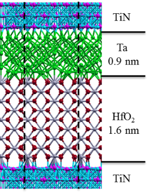
The modeled virgin TiN-HfO2 heterostructure with a Ta insertion layer is shown in Figure 1. The virgin structure is the reference structure with stoichiometric HfO2 and no defects or oxygen vacancies.

We have considered eight prototype states in two equal sets, the first set without a Ta scavenger layer and the second one with the layer (Fig. 2). We will refer to either the TiN electrode in the first set or the TiN-Ta in the second set as “electrode”, and when we speak of the “interface” between the oxide and the electrode, we refer to the oxide-TiN interface in the first set, and the oxide-Ta interface in the second set. Each set of states contains a virgin state with stoichiometric pristine cHfO2 representing the off-state as a reference. Three atomic configurations within each set are used to represent the on-state. In these on-states a linear oxygen vacancy filament is simulated by removing one adjacent oxygen atom from each of the nine HfO2 layers. This linear filament model of oxygen vacancy is similar to that adopted for monoclinic HfO2 (mHfO2) to study the quantized conductance observed for HfO2 Long et al. (2013). The nine removed oxygen atoms are either simply taken out of device, simulating the oxygen-escaped state (see Table 2), or placed at the interface between electrode and HfO2 (“O at interface” in Table 2), or distributed inside the electrode (“O inside electrode” in Table 2). These three cases are used to represent three ideal extremes of the device state. The energies per moved oxygen atom of the on-states relative to virgin TiN-cHfO2-TiN and TiN-cHfO2-Ta-TiN reference states are summarized in Table 2. For each device set (either with or without Ta scavenger layer), the relative energy of one device state ( or , ) is calculated by the total energy difference between this state and the corresponding virgin state (), i.e, , where and are the total energies of the given device state and the virgin state, respectively (and analogously for the primed states). Note that for the states 2 and 2’ for which oxygen escapes from device, the total energy is calculated by adding the total energy of the remaining device to the formation energy of the oxygen molecules.
| TiN-HfO2-TiN | TiN-Ta-HfO2-TiN | |
|---|---|---|
| Virgin state (No Vo) | 0.00 (Model 1) | 0.00 (Model 1’) |
| O escaped | 7.40 (Model 2) | 7.51 (Model 2’) |
| O at interface | 3.63 (Model 3) | 2.09 (Model 3’) |
| O inside electrode | 8.93 (Model 4) | 3.18 (Model 4’) |
When oxygen is placed at the TiN-HfO2 interface, oxygen atoms move towards HfO2 and form bonds with Hf during the geometry relaxation process, avoiding the TiN. In contrast, when oxygen atoms are placed at the Ta-HfO2 interface they move to and bind with Ta (left bottom panel, Fig. 2). As oxygen has a very low solubility in TiN, we model the oxygen inside TiN (Model 4) by calculating the energy of placing one oxygen atom inside TiN bulk (modeled by a cubic box with side length of about 1.1 nm) and multiplying the total energy difference of the model with and without oxygen atom by nine. For the case where oxygen is distributed inside Ta, oxygen atoms are placed at the interstitial sites in the five Ta layers (right bottom panel, Fig. 2). Our results show that the virgin device state without a conducting filament is the most stable state thermodynamically, with or without Ta scavenger layer (Table 2). This implies that an appreciable energy needs to be supplied by electric field to move oxygen from their initial positions in HfO2.
The hypothetical case of oxygen atoms escaping device and forming O2 molecules is an endothermic process with an energy cost as high as 7.5 eV (per O atom) for the modeled systems, both with and without tantalum layer. The effect of the Ta oxygen scavenger layer is clear if oxygen is assumed to remain in the system without escaping to the atmosphere: when oxygen is moved from HfO2 to the Ta-HfO2 interface, the energy cost is calculated to be as low as 2.1 eV. This is less than two thirds of the corresponding energy cost of moving the oxygen to the TiN-HfO2 interface (3.6 eV). This means a significantly lower cost in energy for removing oxygen from the HfO2 matrix when the Ta oxygen scavenger layer is inserted. Interestingly, similar trend has been observed experimentally, i.e., by inserting an Hf layer between TiN and HfO2 the forming bias is reduced from 4 eV to about 2 eV Stefano et al. (2013).
In contrast, the energy cost for moving oxygen into the TiN electrode is forbiddingly high (8.9 eV), which is even larger than that of oxygen escaping to the ambient atmosphere. Thus, once the interface is saturated with oxygen, further removal of oxygen from the HfO2 is highly unfavorable, making the formation of an oxygen vacancy filament difficult in a HfO2-TiN structure without scavenger layer. On the other hand, it is much easier for oxygen to move into Ta, with a much smaller energy cost (3.2 eV) than for moving into TiN. The lower energy cost for moving oxygen into the scavenger layer implies significantly improved switching properties in the presence of the scavenger layer by avoiding oxygen piling up at the electrode-HfO2 interface, which restrains the formation of an oxygen-deficient phase in HfO2. The inserted Ta oxygen scavenger layer thus works as a potential trap for oxygen, restraining oxygen from either escaping out of device or moving into the TiN electrode. As a result, oxygen is constrained to the active region near the electrode-oxide interface during device operation, potentially leading to a reduction of device variance and enhanced device endurance.
III.2 Energy band offsets
We will now discuss the electronic structure of the MIM structures to elucidate the effect of the Ta insertion and location of diffused oxygen on the electronic structure. As we showed in the previous section, the on-states with Ta are favorable thermodynamically over the on-states without Ta, so we will therefore mostly focus on the on-states with Ta. We will study the virgin states both with and without Ta insertion layer (Models 1 and 1’), the lowest-energy on-state without Ta (Model 3), as well as the on-states with Ta (Models 2’, 3’ and 4’). We are specifically interested in how the energy levels of the sandwiched oxide are aligned with those of the metallic electrodes for the different proototypical systems.
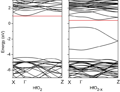
Our model systems all have nine HfO2 atomic layers with a total thickness of 1.6 nm sandwiched between electrodes in each model. We first show the band structures we obtained for isolated HfO2, both in the stoichiometric form and in the reduced form, in Fig. 3. Note that we will always assign zero of energy to the Fermi level. The electronic states near the Fermi level for the reduced HfO2 are found to be dominated by vacancy-induced states, which form new mid-gap bands (right panel of Figure 3). As a result, the calculated energy gap is reduced from 5.4 eV to 0.8 eV, and there is a small density of states below the Fermi level but above the valence bands.
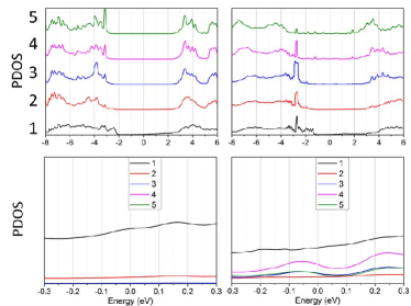
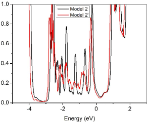
We use the projected density of states (PDOS) of the central HfO2 layer (layer 5) to investigate the electronic structure of the sandwiched HfO2; in contrast with the central layer, the electronic states of the HfO2 layers in direct contact with the electrodes hybridize with those of the electrodes, such that the local electronic structure and PDOS are strongly influenced by the electrodes. We show the evolution of the PDOS from the interface region to the central HfO2 bulk region of Models 1 and 3 as examples in Fig. 4. For the first two HfO2 layers from the interface, layers 1 and 2, the local energy gap is closed even for Model 1, with an appreciable PDOS around the Fermi level (lower panels). From layer 3, the PDOS starts to converge to its values in the bulk region. In Models 2’ - 4’ each layer in the HfO2-x has a finite density of states (DOS) at the Fermi energy, Ef, indicating metallic properties across the reduced oxide film (not shown). In addition, the contact of HfO2-x with Ta-TiN electrodes appears to induce small but finite PDOS throughout the energy range from the valence band maximum (VBM) to the conduction band minimum (CBM), which effectively closes energy gap as shown for the central layer PDOS in Fig. 5. This implies a weak metallic temperature dependence of the on-state and is consistent with the experimental observation that a scavenger layer reduces the temperature dependence of the on-stateStefano et al. (2013).
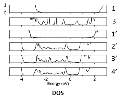
We now address the energy band offset and Schottky barrier height (SBH) by analyzing the PDOS of the sandwiched oxide film (Fig. 5). The device Fermi level is set by the TiN electrodes, which are semi-infinite on both sides of the sandwiched oxide. For the virgin states (Models 1 and 1’) there is a clear gap of about 5 eV as in bulk HfO2 (cf. Fig. 3, left panel), but the inserted Ta layer shifts the PDOS downward in energy (Model 1’). The location of the CBM of the oxide with respect to the Fermi level gives the SBH. The SBH are 2.4 and 1.7 eV for Models 1 and 1’, respectively, indicating a down-shift of 0.7 eV of the PDOS spectrum upon Ta insertion. For the on-state Model 3 without Ta, the CBM (and VBM) is shifted down in energy about 1 eV relative to the virgin state (Model 1), and there is a small but non-zero PDOS at the Fermi level , in addition to isolated PDOS peaks below . For the on-states with Ta (Models 2’, 3’, and 4’), the CBM is shifted down about 1.25 eV compared to the virgin state Model 1’. In addition there appear electron states induced in the gap region as a result of reduction of the HfO2. The PDOS at Ef is again finite as in Model 3, which indicates metallic properties. However, in contrast with Model 3, there is now a finite PDOS in the entire energy range from CBM (at about 0.75 eV above ) to about 3 eV below . We also note that there are no significant differences in the PDOS spectra of Models 2’, 3’ and 4’, with PDOS peaks at approximately the same energies for all these three models. This shows that the energy band offset is insensitive to the distribution of the diffused oxygen atoms in the presence of the Ta oxygen scavenger layer.
Our results are consistent with recent experimental work on the effect of inserting a hafnium layer between TiN and HfO2 Afanas’ev et al. (2011). In Ref. Afanas’ev et al. (2011) it was observed that the SBH of the TiN-HfO2 heterostructure was reduced by about 1 eV with the insertion of an Hf inter-layer, and attributed the SBH reduction to a surface dipole induced by oxygen scavenging by the inserted Hf layer. We will now show that our simulation strongly supports this conjecture. We plot the charge distribution across the electrode-HfO2 interfaces of selected models in Fig. 6. We begin our analysis by discussing Models 1 and 1’ [panel (a) in Fig. 6], which contain insulating stoichiometric HfO2. The value of the SBH, or more generally, how the energy bands of the oxide are aligned with those of the electrode, is determined by the effective interface dipole Tung (2014). Figure 6 (a) shows that without Ta insertion (Model 1), a negative charge appears on the electrode side, while there is a positive charge on the oxide side. As a result, an interface electric dipole is induced, pointing from electrode to oxide. In contrast, when Ta is inserted (Model 1’), there is a positive charge on the electrode (Ta) side and a negative charge on the oxide side, with the effective electric dipole pointing from oxide to electrode. This reflects the fact Ta has a strong tendency to lose electrons, because of its low electronegativity, compared to TiN. The net effect of inserting Ta between TiN and HfO2 is then a downward shift in energy of the average electrostatic (Hartree) potential energy in Model 1’, compared to Model 1, as seen in Fig. 6 (b). This downward shift is about 0.7 eV, which is approximately equal to the downward shift in the SBH from Model 1 to Model 1’. Indeed, we obtain a decrease of 0.7 eV of the SBH of the virgin states [Models 1 and 1’, Fig. 5] when Ta is inserted, which is comparable to the experimental value of 1 eV obtained for Hf-HfO2 Afanas’ev et al. (2011).
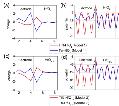
For the on-states with reduced HfO2, inserting Ta has a similar effect on the charge redistribution at the electrode-oxide interface [Fig. 6 (c)]. However, both for Models 2 and 2’ the induced charge on the electrode side is reduced (smaller in magnitude for Model 2 and more negative for Model 2’) compared to the charge in the virgin states Models 1 and 1’. (We are here using Models 2 and 2’ as they provide for a better comparison of what inserting Ta does than the other models with reduced oxide.) However, the electrostatic potential energies rapidly become equal in the reduced oxide [Fig. 6 (d)].
In contrast with stoichiometric HfO2, reduced HfO2-x is metallic. When coupled with the electrodes, Ef of HfO2-x and Ef of electrodes must match each other to form the common Fermi level of the device. Thus, the PDOS for HfO2-x shifted in energy relative to that of HfO2, with a magnitude of the shift determined by enforcing local charge neutrality. An electric field induced by an interface dipole is screened by free electrons in HfO2-x. All modeled on-states with Ta show similar energy level alignment between oxide and electrodes (Models 2’, 3’ and 4’, Fig. 5), irrespective of where the diffused oxygen atoms are located. Furthermore, the Ta insertion has little effect on the PDOS for the reduced oxide when the oxygen is not at the oxide-electrode interface, as shown for Models 2 and 2’ in Fig. 7. (Oxygen at the TiN-HfO2-x interface, Model 3, severely distorts the interface structure, which affects PDOS below , as seen in Fig. 5.)
III.3 Transport properties
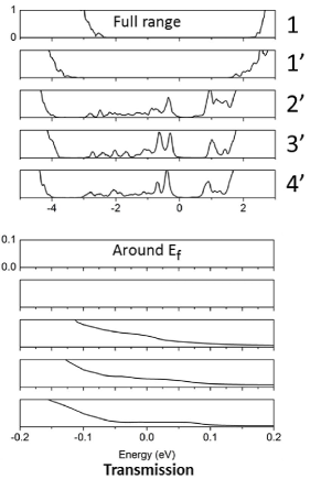
Our calculated transmission spectra for the MIM structures (Fig. 8 “Full range”) show a clear correlation with the DOS of the sandwiched oxide film in Fig. 5. For the virgin states, the location of spectrum gap is very similar both in the transmission spectrum and in the PDOS spectrum. The values of the SBH estimated from the transmission spectra are nearly the same as those obtained from PDOS of the central oxide layer. Similarly, for the on-states major transmission peaks have similar locations as the peaks in PDOS across the different models.
| Model | l | 1’ | 2’ | 3’ | 4’ |
| Conductance | 3.7E-6 | 5.2E-6 | 6.3E-2 | 6.3E-2 | 3.6E-2 |
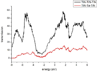
We now discuss the low-bias conductance of selected models. We focus on transmission in an energy range from Ef-0.2 eV to Ef+0.2 eV (Fig. 8 “Around Ef”). The virgin states show negligible transmission in this energy range, signaling transport only through quantum tunneling. The on-states in contrast show finite transmission at Ef, consistent with metallic properties. In order to quantitatively compare the conductances of the different models, we list their low-bias conductances in Table 3, in which the conductance is estimated by averaging the transmission in an energy range from Ef-0.2 to Ef+0.2 eV. For the virgin states, transport under low bias falls into the tunneling regime, with transmission at Fermi level on the order of per nm2. Although the SBH is reduced by 0.7 eV when Ta is inserted, the effect on the low-bias transport is small: the estimated conductance of Models 1 and 1’ is of the same order of magnitude. The tendency of enhanced tunneling current with reduced SBH when Ta is inserted is offset by electron scattering because of the band mismatch at the additional TiN-Ta interface. This is illustrated in Fig. 9, which compares the transmission functions of two hypothetical structures, both with TiN electrodes. The TiN-TiN-TiN structure consists of a TiN part in the central scattering region, which of course couples seamlessly with two TiN electrodes without any interfacial scattering. As a result, electrons in the whole energy range can be transmitted in a “reflectionless” way, i.e., without any scattering. Therefore, the transmission function for the TiN-TiN-TiN structure just reflects the DOS properties of TiN. In contrast, the mismatch of band structure between Ta and TiN results in a decreased transmission function for the TiN-Ta-TiN structure in the whole energy range compared to the reflectionless TiN-TiN-TiN structure.
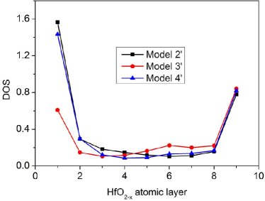
For the on-states, all structures (Models 2’ to 4’) exhibit low-bias conductance on the order of per nm2, which is four orders of magnitude greater than that of the virgin states. Thus, the conductivity of the modeled on-states has no strong dependence on the location of diffused oxygen atoms. We note that diffused oxygen either inside Ta or at the Ta-oxide interface induces variations in the magnitude of available PDOS near the Fermi level across HfO2-x layers (Fig. 10). However, each atomic layer has a non-zero PDOS near . As a result, the on-states are metallic, regardless of the location of the diffused oxygen.
IV CONCLUSION
In summary, we have investigated the behavior of TiN-HfO2-TiN and TiN-HfO2-Ta-TiN heterostructures with a goal of elucidating the role of the Ta oxygen scavenger layer on thermodynamic stability, electronic structure and transport. We find that the presence of the Ta layer improves the stability of the reduced oxide system, in which oxygen has been depleted from the HfO2, and facilitates the formation of conducting channel in the oxide, consistent with experimental workAfanas’ev et al. (2011). Furthermore, the Ta layer reduces the Schottky barrier height for the insulating system because of a different interface charge at the Ta-HfO2 interface than at the TiN-HfO2 interface. Nevertheless, the reduced Schottky barrier height does not negatively impact the on-off ratio. Also, the electronic structure of the reduced oxide with a Ta layer becomes insensitive to the location of the oxygen atoms that are removed from the stochiometric oxide, with the consequence that the low-bias conductance in the on-state is insensitive to the location of the oxygen atoms. This is in contrast with the structure without a Ta layer, for which the electronic structure can vary quite significantly, depending on where the oxygen atoms are located. These results are consistent with experimental observations that a scavenger layer reduces the dispersion of on/off resistance ratioChen et al. (2013).
Our results, which are based on detailed density functional-theory calculations using the GGA+U approximation, explain experimental resultsMiyazaki et al. (2014) that demonstrate better device performance, in particular how the Ta layer facilitates the formation of conducting filaments, and how the Ta layer can lead to more robust devices, that is, less dependence on the microstructure of the device in its on-state. These results provide a firm foundation for further studies of oxygen scavenger layers of different thickness and chemical composition as enablers for realizing low-power resistive random access memory technologies.
Acknowledgements.
The work by X.Z. and O.H. was supported by U. S. DOE, Office of Science under Contract No. DE-AC02-06CH11357. P.Z. acknowledges support from the U.S. Department of Energy, Office of Science, Materials Sciences and Engineering Division. I.R. acknowledges financial support from the European Union’s Horizon2020 research and innovation programme within the PETMEM project. We gratefully acknowledge the computing resources provided on Blues and Fusion, high-performance computing clusters operated by the Laboratory Computing Resource Center at Argonne National Laboratory.References
- Yang, Strukov, and Stewart (2013) J. J. Yang, D. B. Strukov, and D. R. Stewart, Nat. Nanotechnol. 8, 13 (2013).
- Yang et al. (2009) J. J. Yang, F. Miao, M. D. Pickett, D. A. A. Ohlberg, D. R. Stewart, C. N. Lau, and R. S. Williams, Nanotechnology 20, 215201 (2009).
- Stefano et al. (2013) F. D. Stefano, M. Houssa, V. V. Afanas’ev, J. A. Kittl, M. Jurczak, and A. Stesmans, Thin Solid Films 533, 15 (2013), {EMRS} 2012 Symposium L.
- Prócel et al. (2013) L. Prócel, L. Trojman, J. Moreno, F. Crupi, V. Maccaronio, R. Degraeve, L. Goux, and E. Simoen, J. Appl. Phys. 114, 074509 (2013).
- Nakamura et al. (2014) H. Nakamura, T. Miyazaki, K. Nishio, H. Shmia, H. Akinaga, and Y. Asai, in Computational Electronics (IWCE), 2014 International Workshop on (2014) pp. 1–3.
- Yajima et al. (2010) T. Yajima, K. Fujiwara, A. Nakao, T. Kobayashi, T. Tanaka, K. Sunouchi, Y. Suzuki, M. Takeda, K. Kojima, Y. Nakamura, K. Taniguchi, and H. Takagi, Jpn. J. Appl. Phys. 49, 060215 (2010).
- Cartoixà, Rurali, and Suñé (2012) X. Cartoixà, R. Rurali, and J. Suñé, Phys. Rev. B 86, 165445 (2012).
- Long et al. (2013) S. Long, X. Lian, C. Cagli, X. Cartoixà, R. Rurali, E. Miranda, D. Jiménez, L. Perniola, M. Liu, and J. Suñé, Appl. Phys. Lett. 102, 183505 (2013).
- Miyazaki et al. (2014) T. Miyazaki, H. Nakamura, K. Nishio, H. Shima, H. Akinaga, and Y. Asai, in JPS Conference Proceedings, Vol. 1 (2014) p. 2075.
- Kamiya et al. (2012) K. Kamiya, M. Y. Yang, S.-G. Park, B. Magyari-Köpe, Y. Nishi, M. Niwa, and K. Shiraishi, Appl. Phys. Lett. 100, 073502 (2012).
- Hohenberg and Kohn (1964) P. Hohenberg and W. Kohn, Phys. Rev. 136, B864 (1964).
- Kohn and Sham (1965) W. Kohn and L. J. Sham, Phys. Rev. 140, A1133 (1965).
- Perdew, Burke, and Wang (1996) J. P. Perdew, K. Burke, and Y. Wang, Phys. Rev. B 54, 16533 (1996).
- Czyżyk and Sawatzky (1994) M. T. Czyżyk and G. A. Sawatzky, Phys. Rev. B 49, 14211 (1994).
- Soler et al. (2002) J. M. Soler, E. Artacho, J. D. Gale, A. García, J. Junquera, P. Ordejón, and D. Sánchez-Portal, J. Phys. Condens. Matter 14, 2745 (2002).
- Rungger and Sanvito (2008) I. Rungger and S. Sanvito, Phys. Rev. B 78, 035407 (2008).
- Rocha et al. (2005) A. R. Rocha, V. M. Garcia-Suarez, S. W. Bailey, C. J. Lambert, J. Ferrer, and S. Sanvito, Nature Mater. 4, 335 (2005).
- Rocha et al. (2006) A. R. Rocha, V. Garcia-Suarez, S. Bailey, C. Lambert, J. Ferrer, and S. Sanvito, Phys. Rev. B 73, 085414 (2006).
- Pemmaraju et al. (2007) C. D. Pemmaraju, T. Archer, D. Sánchez-Portal, and S. Sanvito, Phys. Rev. B 75, 045101 (2007).
- Zhong et al. (2015) X. Zhong, I. Rungger, P. Zapol, and O. Heinonen, Phys. Rev. B 91, 115143 (2015).
- Park, Magyari-Köpe, and Nishi (2010) S.-G. Park, B. Magyari-Köpe, and Y. Nishi, Phys. Rev. B 82, 115109 (2010).
- Broqvist and Pasquarello (2006) P. Broqvist and A. Pasquarello, Appl. Phys. Lett. 89, 262904 (2006).
- Troullier and Martins (1991) N. Troullier and J. L. Martins, Phys. Rev. B 43, 1993 (1991).
- Pflüger et al. (1984) J. Pflüger, J. Fink, W. Weber, K. P. Bohnen, and G. Crecelius, Phys. Rev. B 30, 1155 (1984).
- Passerini (1930) L. Passerini, Gazz. chim. ital 60, 762 (1930).
- Waseda, Hirata, and Ohtani (1975) Y. Waseda, K. Hirata, and M. Ohtani, High Temp. High Press. 7, 221 (1975).
- Oh et al. (2013) Y. J. Oh, A. T. Lee, H.-K. Noh, and K. J. Chang, Phys. Rev. B 87, 075325 (2013).
- Jiang et al. (2010) H. Jiang, R. I. Gomez-Abal, P. Rinke, and M. Scheffler, Phys. Rev. B 81, 085119 (2010).
- Gavartin et al. (2006) J. L. Gavartin, D. Muñoz Ramo, A. L. Shluger, G. Bersuker, and B. H. Lee, Appl. Phys. Lett. 89, 082908 (2006).
- Cimino et al. (2012) S. Cimino, A. Padovani, L. Larcher, V. Afanas’ev, H. Hwang, Y. Lee, M. Jurczac, D. Wouters, B. Lee, H. Hwang, and L. Pantisano, Microelectron. Eng. 95, 71 (2012).
- Fonseca and Knizhnik (2006) L. R. C. Fonseca and A. A. Knizhnik, Phys. Rev. B 74, 195304 (2006).
- Afanas’ev et al. (2011) V. V. Afanas’ev, A. Stesmans, L. Pantisano, S. Cimino, C. Adelmann, L. Goux, Y. Y. Chen, J. A. Kittl, D. Wouters, and M. Jurczak, Appl. Phys. Lett. 98, 132901 (2011).
- Tung (2014) R. T. Tung, Appl. Phys. Rev. 1, 011304 (2014).
- Chen et al. (2013) C. Chen, S. Gao, F. Zeng, G. Tang, S. Li, C. Song, H. Fu, and F. Pan, J. Appl. Phys. 114, 014502 (2013).