Infrared light emission from atomic point contacts
Abstract
Gold atomic point contacts are prototype systems to evidence ballistic electron transport. The typical dimension of the nanojunction being smaller than the electron-phonon interaction length, even at room temperature, electrons transfer their excess energy to the lattice only far from the contact. At the contact however, favored by huge current densities, electron-electron interactions result in a nano hot electron gas acting as a source of photons. Using a home built Mechanically Controlled Break Junction, it is reported here, for the first time, that this hot electron gas also radiates in the infrared range (0.2eV to 1.2eV). Moreover, in agreement with the pioneering work of Tomchuk [1],we show that this radiation is compatible with a blackbody like spectrum emitted from an electron gas at temperatures of several thousands of Kelvin given by where , and are respectively a fitting parameter, the current flowing and the applied bias.
1 Introduction
Understanding and managing the interplay between electrons and photons around the Fermi level is of paramount importance for both fundamental and applied solid states physics. The recent intense research works in the field of nanoantennas [2] or regarding light-emitting diode droop see [3], and references therein. illustrate this importance. As the sizes of the active regions shrink to the nanometre scale, as local current densities increase, new processes, previously not favoured, are put forward, intentionally or not.
The tip of a scanning tunneling microscope has been used to inject electrons and to promote local light emission from semiconductor quantum structures [4, 5, 6] or from single molecules [7]. These STM light emission (STM-LE) works followed the pioneering work of J.Gimzewski’s group on metals [8, 9]. For metals, in the conductance range, the well-accepted dominant one-electron mechanism is the following [10]: an inelastic tunneling electron excite collective electron modes of the tip-gap-surface nanocavity. These modes depend on the geometry of the cavity at the nanoscale and on the dielectric properties of the metals [11]. These electromagnetic modes relax their energy mainly to the phonons but also through photon emission. The two key features of the emitted spectra are i) that they exhibit plasmonic resonances typical of the cavity and metals-dependent, and ii) that the high energy part of the spectra is limited by the energy carried by a tunneling electron () [12]. Although it is obviously not possible to know the tip shape at this scale, and thus the electromagnetic modes due to the tip-gap-surface nanocavity, it has been shown that rationalizing spectra acquired with the same tip on different areas or at different bias conditions could provide useful physical information respectively on the material below the tip [13, 7] or on the carrier density [14].
Indeed photons with energies exceeding the so-called quantum cutoff ”limit” of have also been observed in STM-LE regime [15, 16]. Such photon energies are still observed at higher conductances, above in the Atomic Point Contact Light Emission (APC-LE) regime [17, 18]. The emission of these photons evidences the importance of multi-carrier excitation processes.
During the last decades, atomic sized metallic conductors have been extensively studied [19], a prototype system being the well-known stretched gold nanowire. Under electrical polarization, prior being broken, the conductance of such a wire exhibits characteristic Landauer plateaus at integer multiples of [20, 21]. Along these plateaus the conductance remains constant despite the length increase of the metallic nanowire. Indeed, while the length of the nanoconstriction is much smaller than the electron-phonon interaction length [22], no extra-resistance is added to the contact resistance. Moreover, considering only electron-phonon scattering, the electron injected from one contact to the other will preserve his energy and momentum over ballistic distances of the order of . The order of magnitude of is given by:
| (1) |
with the Fermi velocity, Debye frequency and , the electron-phonon coupling factor () [22]. However, these gold nanoconstrictions are the siege of huge current densities ( A.m-2) and electron-electron interactions play a significant role in redistributing the energy of the electrons [23].
As mentioned above, APC-LE is also observed. The spectra show the presence of photons with energy above the polarisation energy eV of electrons [17, 18, 24]. The emission of these photons evidences the importance of multi-carrier excitation processes resulting in a hot carriers energy distribution spreading over more than .
From their first observations, A. Downes [17] have put forward the radiative emission from of a hot electron gas. Consistently with previous works on systems with analogue physics by Fedorovitch (see [25] and references therein), electron temperatures of the order of K were extrapolated fitting the corrected emission spectra by a black-body behaviour. Applying a 1 volt bias, at a conductance of , photons with energy above 2.5 eV were detected. Although most spectra were featureless in the visible range, modulation or intense peaks, evoking electromagnetic resonances of the tip-gap-surface nanocavity were sometimes observed. These experiments were performed with an STM in ultra high vacuum (UHV), at K. In similar conditions, but at 4 K, G. Schull [18] also reported light emission above the quantum cutoff. However, their results are different from two important points of view: i) the spectra exhibit resonance features similar to what is commonly observed in STM-LE and ii) no photon of energy above twice eV is observed. The high energy part of the spectra is also attributed to hot electrons, hotter than eV, excited through an Auger-like two charge carriers cascade mechanism. A mechanism consistent with photon energies between eV and 2eV.
Recently, M. Buret [24] also reported black-body like emission from electroformed gold junction at conductance values of the order of . As in [17], they also observed photons with energy above consistent with a black-body like radiation of an hot electron gas. Electronic temperatures, , above 1500 K, i.e. well above the gold melting point ( K), are indirectly measured. They propose a mechanism involving gold interband reabsorption by low-lying d-band electrons to explain the apparent experimental discrepancy with [18].
Using a home-build Mechanical Controlled Break Junction (MCBJ) [26], we have been revisiting APC-LE both in the visible range and, for the first time, in the near infra-red (IR) range of the spectrum. This article focuses on the IR range. We report intense IR emission, conterbalancing the known relatively poor sensitivity of IR detectors. We also report basic spectroscopic data, supporting a blackbody-like emission from hot electron gas.
One of the reasons for focusing on the emission in the IR range is that we do not expect electromagnetic plasmonic resonances comparable to what is observed in the visible range. In the classical theory [11] we would expect a diverging redshift of these resonances as the distance between electrodes is reduced from the STM regime down to the contact regime. Noteworthy, to our knowledge, this redshift was never observed. Indeed, recent quantum approaches have theoretically predicted [27, 28] and experimentally demonstrated [28] a non monotonous behaviour, limiting the wavelength of the resonances below 1 micron.
2 Experimental set-up
For these experiments, the setup consists of i) a MCBJ ii) the light collection
and detection components and iii) the acquisition and control electronics and
informatics (see fig.1).
The MCBJ was first introduced by Ruitenbeek et al [29]. For
these studies, our is operated in air and at room temperature. The mechanical
part is similar to the one we described previously [26], although
the sample preparation technique has been since improved. The separation of the
electrodes is controlled by a micrometer step motor stacked-up with a
piezoelectric actuator (sensibility : ). Motor and piezo are
driven through an input/output (IO) board by a computer interface (written with
Labview) that is also used for acquiring data and feedback (see below). Taking
into account a typical push:stretch ratio of 20:1 and the resolution of our
16-bit DAC, one digit corresponds to less than which is quite enough for
this work.
The junction, in series with a ballast resistor is biased from the
IO board. The conductance is derived from the measured intensity that flows
through the junction using a current/voltage converter (DLPCA-200, FEMTO) with
a A/V transconductance gain.
At low bias ( ), in air and at room temperature, atomic
contacts often remain stable for tens of seconds [26].
Figure2 illustrates the long term stability of junctions biased
at low voltage. As the bias is increased up to values stimulating light
emission, the lifetime of monoatomic contacts decreases drastically below .
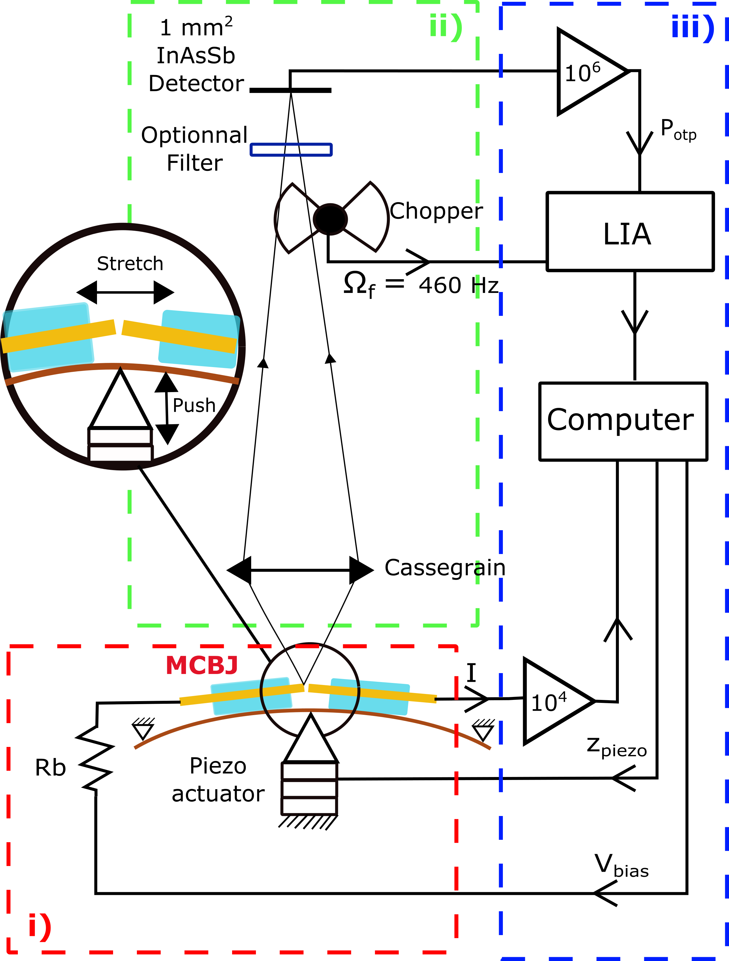
To collect infra-red photons, we are using a Cassegrain microscope objective (x15 ; ). The optical beam is mechanically chopped at , transmitted through a semiconductor filter and measured by a cooled InAsSb detector (P11120-201, Hamamatsu) sensitive from to , using a lock-in amplifier (HF2LI, Zurich Instruments) . We use silicon and germanium wafers of respective gap and as lowpass filters to gather first-order spectroscopic data.
To measure an optical IR signal we operate with an input electrical power in the mW range. More precisely, we apply a bias in the volt range and drive the MCBJ at conductance of a few . The MCBJ device is mechanically and thermally stable at the macroscopic scale. Moreover, taking advantage of thermal diffusion and electromigration, at room temperature, the nanojunction self-organises at atomic level and naturally explores the more stable configurations around the average chosen conductance value. We thus only need a loose feedback using the piezo actuator to maintain the conductance between .
3 Results
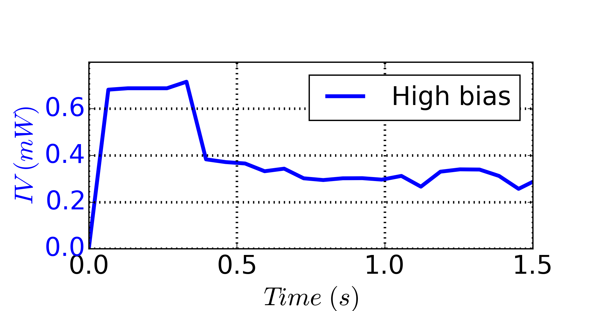
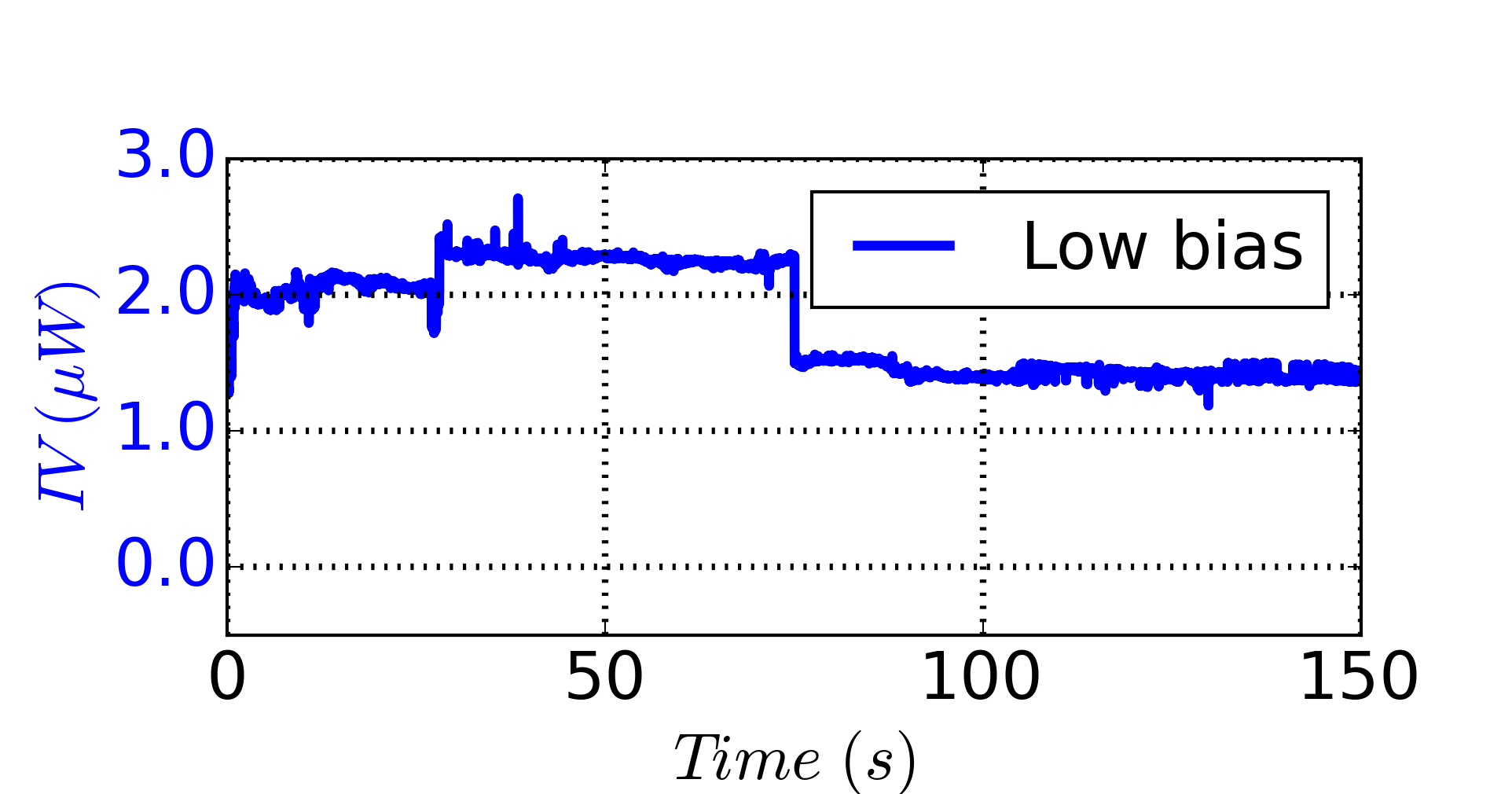
While we deliberately drive our MCBJ in a loose feedback mode, its conductance naturally varies during the experiments. We have plotted (figure 2) the fluctuation of electrical power , which is a relevant parameter [25], as a function of time. It shows that the applied bias and the stability are negatively correlated. A compromised to measure an optical signal thus has to be found.
Figure.3 plots together the temporal evolution of the measured electrical power and optical signal. The optical response, measured without optical lowpass filters, appears to be strongly correlated with the electrical power injected in the junction and slightly time-delayed. Cross-correlation (figure 3, inset) of both signals allows to quantify this time lag () which is due to the integration time of the optical signal.
The important result at this point is that an IR signal emitted from the APC is detected. Noteworthy this signal is detected despite the lower sensitivity of optical sensors in the IR range, to be compared with the sensitivity of the sensors in the visible range.
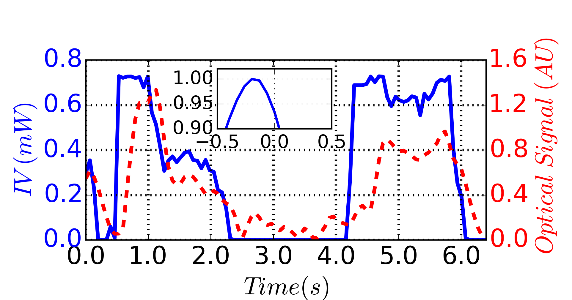
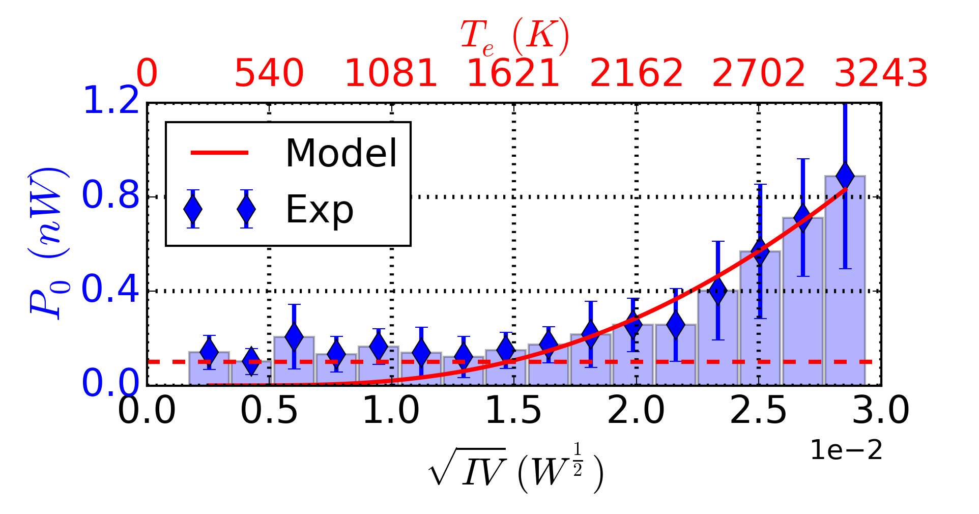
Taking into account the time lag, figure 4 shows the dependence of the optical signal with the electrical power injected in the APC. We superimposed (red continuous line), the result of the expected dependence of the IR signal modeled assuming black body emission as previously proposed [17]. We will come back to this point in the Discusion section.
The above data is acquired using the full bandwidth of the IR detector. To get some basic spectroscopic informations we use semiconductor lowpass filters. The smaller the gap the narrower the optical bandwidth. Table 1 shows the results acquired in the mW regime ( , ).
| Filters | Raw Data (A.U.) |
|---|---|
| Full Output | |
| Si gap | |
| Ge gap |
The data reported in table 1 evidences that half of the signal arises from photons with energies lower than the Ge band gap. From this table, by difference, we construct table 2 to estimate the proportion of signal in each three spectral bands. Table 2 also includes a column of computed values that will be described in the discussion.
| Spectral Bands (eV) | Measurement | Calculus |
|---|---|---|
| Full band | ||
Figure 5 shows a black-body spectrum (), convoluted by the detector spectral response. The three different spectral bands corresponding to the use of the optical filters are represented by grey-scale bands below the black-body spectrum. Integrating the optical signal for these spectral bands allows the calculatation the expected signal reported in the appropriate column of table 2.
4 Discussion
As mentioned above, APC-LE has been attributed to the radiation from a hot electron gas [17, 18, 24]. The associated observed spectrum was proposed to correspond to a black-body like emission from a high temperature () system[25, 17, 24]. Such an emission spectrum obeys :
| (2) |
with being the optical luminance, the temperature, the photon energy, the Boltzmann constant and the light velocity. Tomchuk and Fedorovich showed [1] that the electronic temperature in isolated metal island, with dimension below , could be related to the lattice temperature and electrical power following the equation:
| (3) |
Here is the current and the applied bias and an empirical constant describing the heating efficiency.
Assuming , we can write :
| (4) |
Taking into account the spectral response and bandwidth of the detector, integrating the optical luminance and normalizing, we compute the optical power :
| (5) |
The continuous red line of fig.4 is computed from this expression, being the only fitting parameter. The fit was obtained for .
From the fitted and measured values we can calculate the electronic temperature from . This values are reported on the top axis of fig.4. In standard operating conditions of the MCBJ (i.e. conductance of a few ), of several thousands of degrees, far exceeding , are found and fortify the above assumptions.
From an experiment corresponding to , knowing the fitted an thus the hot electron gas temperature using eq.4 we plot the expected black-body spectrum (figure 5 dashed curve).
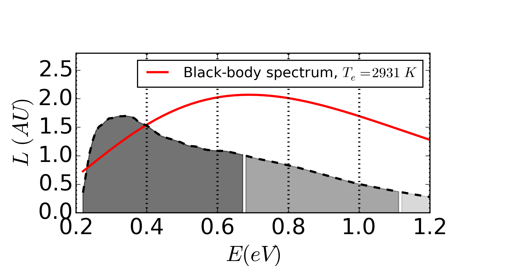
From it, taking into account the detector response and the properties of the three lowpass optical filters, we compute the three expected normalised optical powers, using:
| (6) |
with and being the lower and upper energy limit of the considerate
spectral band. These computed values are reported in the last column of
table.2. The agreement with the measured signal is excellent. We point
out that, although basic, the spectroscopic analysis gives useful results
corroborating the black-body model of the emission source.
Moreover the proportion of signal below and above the germanium bandgap can only be consistent with black-body temperatures far above the Au fusion temperature of .
5 Conclusion and Perspectives
In this letter, we have reported for the first time the observation of IR light emission from metallic point contacts. Results are quantitatively consistent with the emission of a hot electron gas which temperature exceeds the melting point of gold. They also prolongate the conclusions previously made, at lower input power on the basis of the light detected in the visible range, by A.Downes et al. [17] and by M.Buret et al.[24]. The spectroscopic analysis is already very useful and we forecast that in a near future the stability of APC at ambient temperature will allow to use more advanced and enlightening tools (such as Fourier Transform Infra-Red spectroscopy).
Acknoledgements
We thank Mehdi Lagaize for technical support.
References
- [1] P. M. Tomchuk and R. D. Fedorovich. Emission of hot electrons from thin metal films. Soviet Physics-Solid State, 1966.
- [2] Lukas Novotny and Niek Van Hulst. Antennas for light. Nature Photonics, 5(2):83–90, 2011.
- [3] Justin Iveland, Lucio Martinelli, Jacques Peretti, James S Speck, and Claude Weisbuch. Direct measurement of auger electrons emitted from a semiconductor light-emitting diode under electrical injection: identification of the dominant mechanism for efficiency droop. Physical review letters, 110(17):177406, 2013.
- [4] Philippe Renaud and Santos F Alvarado. Mapping quantum-well energy profiles of iii-v heterostructures by scanning-tunneling-microscope-excited luminescence. Physical Review B, 44(12):6340, 1991.
- [5] S Ushioda, T Tsuruoka, and Y Ohizumi. Characterization of surface nanostructures by stm light emission: individual gaas/algaas quantum wells. Applied surface science, 166(1):284–289, 2000.
- [6] Ph Dumas, V Derycke, IV Makarenko, R Houdre, P Guaino, A Downes, and F Salvan. Scanning-tunneling-microscopy-induced optical spectroscopy of a single gaas quantum well. Applied Physics Letters, 77(24):3992–3994, 2000.
- [7] XH Qiu, GV Nazin, and W Ho. Vibrationally resolved fluorescence excited with submolecular precision. Science, 299(5606):542–546, 2003.
- [8] JK Gimzewski, B Reihl, JH Coombs, and RR Schlittler. Photon emission with the scanning tunneling microscope. Zeitschrift für Physik B Condensed Matter, 72(4):497–501, 1988.
- [9] J. K. Gimzewski, J. K. Sass, R. R. Schlitter, and J. Schott. Enhanced photon emission in scanning tunnelling microscopy. EPL (Europhysics Letters), 8(5):435, 1989.
- [10] Richard Berndt, James K Gimzewski, and Peter Johansson. Inelastic tunneling excitation of tip-induced plasmon modes on noble-metal surfaces. Physical review letters, 67(27):3796, 1991.
- [11] R. W. Rendell and D. J. Scalapino. Surface plasmons confined by microstructures on tunnel junctions. In PHYSICAL REVIEW B VOLUME 24, 5 UMBER 6 15 SEPTEMBER, 1981.
- [12] JH Coombs, JK Gimzewski, B Reihl, JK Sass, and RR Schlittler. Photon emission experiments with the scanning tunnelling microscope. Journal of Microscopy, 152(2):325–336, 1988.
- [13] Andrew Downes, Philippe Guaino, and Philippe Dumas. Color mapping by scanning tunneling microscopy: Chemical analysis of metal surfaces. Applied physics letters, 80(3):380–382, 2002.
- [14] NL Schneider, F Matino, G Schull, S Gabutti, M Mayor, and R Berndt. Light emission from a double-decker molecule on a metal surface. Physical Review B, 84(15):153403, 2011.
- [15] R Pechou, R Coratger, F Ajustron, and J Beauvillain. Cutoff anomalies in light emitted from the tunneling junction of a scanning tunneling microscope in air. Applied physics letters, 72(6):671–673, 1998.
- [16] Germar Hoffmann, Richard Berndt, and Peter Johansson. Two-electron photon emission from metallic quantum wells. Physical review letters, 90(4):046803, 2003.
- [17] A. Downes, Ph. Dumas, and M. E. Welland. Measurement of high electron temperatures in single atom metal point contacts by light emission. Applied Physics Letters, 81(7):1252, 2002.
- [18] Guillaume Schull, Nicolas Néel, Peter Johansson, and Richard Berndt. Electron-plasmon and electron-electron interactions at a single atom contact. Physical Review Letters, 102(5), Feb 2009.
- [19] Nicolas Agrait, Alfredo Levy Yeyati, and Jan M. van Ruitenbeek. Quantum properties of atomic-sized conductors. Physics Reports, 377(2–3):81 – 279, 2003.
- [20] AI Yanson, G Rubio Bollinger, HE Van den Brom, N Agrait, and JM Van Ruitenbeek. Formation and manipulation of a metallic wire of single gold atoms. Nature, 395(6704):783–785, 1998.
- [21] Thomas Leoni, Remi Zoubkoff, Sabrina Homri, Nadine Candoni, Petar Vidakovic, Alain Ranguis, Hubert Klein, Andres Saul, and Philippe Dumas. Are conductance plateaus independent events in atomic point contact measurements? a statistical approach. Nanotechnology, 19(35):355401–, 2008.
- [22] Neil W Ashcroft and N David Mermin. Solid state phys. Saunders, Philadelphia, page 293, 1976.
- [23] F Pierre, H Pothier, D Esteve, and MH Devoret. Energy redistribution between quasiparticles in mesoscopic silver wires. Journal of Low Temperature Physics, 118(5-6):437–445, 2000.
- [24] Mickael Buret, Alexander V. Uskov, Jean Dellinger, Nicolas Cazier, Marie-Maxime Mennemanteuil, Johann Berthelot, Igor V. Smetanin, Igor E. Protsenko, Gérard Colas des Francs, and Alexandre Bouhelier. Spontaneous hot-electron light emission from electron-fed optical antennas. Nano Letters, 15(9):5811–5818, 2015. PMID: 26214575.
- [25] R.D. Fedorovich, A.G. Naumovets, and P.M. Tomchuk. Electron and light emission from island metal films and generation of hot electrons in nanoparticles. Physics Reports, 328(2–3):73 – 179, 2000.
- [26] Monzer Alwan, Nadine Candoni, Philippe Dumas, and HubertR. Klein. Statistical evidence of strain induced breaking of metallic point contacts. The European Physical Journal B, 86(6), 2013.
- [27] Isabel Romero, Javier Aizpurua, Garnett W Bryant, and F Javier García De Abajo. Plasmons in nearly touching metallic nanoparticles: singular response in the limit of touching dimers. Optics express, 14(21):9988–9999, 2006.
- [28] Kevin J. Savage, Matthew M. Hawkeye, Rubén Esteban, Andrei G. Borisov, Javier Aizpurua, and Jeremy J. Baumberg. Revealing the quantum regime in tunnelling plasmonics. Nature, 491(7425):574–577, Nov 2012.
- [29] JM Van Ruitenbeek, A Alvarez, I Pineyro, C Grahmann, P Joyez, MH Devoret, D Esteve, and C Urbina. Adjustable nanofabricated atomic size contacts. Review of Scientific Instruments, 67(1):108–111, 1996.