Magneto-excitons in large area CVD grown monolayer MoS2 and MoSe2 on sapphire
Abstract
Magneto transmission spectroscopy was employed to study the valley Zeeman effect in large-area monolayer MoS2 and MoSe2. The extracted values of the valley g-factors for both A- and B-exciton were found be similar with . The samples are expected to be strained due to the CVD growth on sapphire at high temperature (C). However, the estimated strain, which is maximum at low temperature, is only . Theoretical considerations suggest that the strain is too small to significantly influence the electronic properties. This is confirmed by the measured value of valley g-factor, and the measured temperature dependence of the band gap, which are almost identical for CVD and mechanically exfoliated MoS2.
I Introduction
Monolayer transition metal dichalcogenides (TMDs) have recently emerged as an exciting material system in which coupled spin-valley physics can be explored.Wang et al. (2012); Mak et al. (2010); Splendiani et al. (2010); Xiao et al. (2012); Cao et al. (2012); Mak et al. (2012); Zeng et al. (2012); Sallen et al. (2012); Jones et al. (2013); Wu et al. (2013); Xu et al. (2014); Mak et al. (2014) Unlike their bulk form, monolayer TMDs exhibit a direct band gap in a visible spectral range located at two inequivalent valleys.Mak et al. (2010); Splendiani et al. (2010) The spin states are split by a strong spin-orbit interaction, and the order of the spin states is reversed in the valleys as a result of time reversal symmetry. Due to the large spin-orbit splitting, the inter band optical absorption gives rise to well separated A and B-exciton transitions. The selection rules for these transitions are governed by the orbital magnetic moment resulting from the Bloch part of the carrier wave function.Yao et al. (2008) Since the crystal structure of a monolayer TMD lacks an inversion center, the out-of-plane element of the orbital magnetic moment is nonzero and its sign depends on the valley index. This results in optical transitions in polarizations, which involve carriers in the valleys, providing an access to the valley index via optical spectroscopy.Cao et al. (2012); Mak et al. (2012); Zeng et al. (2012); Sallen et al. (2012) Photoluminescence revealed a large degree of circular polarization, Cao et al. (2012); Mak et al. (2012); Zeng et al. (2012); Sallen et al. (2012); Jones et al. (2013) reaching 100% for a resonant excitation,Mak et al. (2012) which is extremely promising with a view to employing the valley pseudospin degree of freedom in novel applications in, e.g., quantum information processing.Xiao et al. (2012); Cao et al. (2012); Mak et al. (2012); Zhu et al. (2011) In this respect, the development of large area monolayer TMDs suitable for large scale device applications is crucial.
The existence of a valley-contrasting magnetic moment opens a possibility of controlling the valley pseudospin with an external magnetic field.Rose et al. (2013); Cai et al. (2013); Kormányos et al. (2014); Ho et al. (2014); Chu et al. (2014); Mitioglu et al. (2015) The application of a magnetic field, perpendicular to the layer lifts the valley degeneracy splitting the exciton transitions. In monolayer TMDs the magnetic moment of the carriers has three possible contributions, (i) intracellular magnetic moment originating from the orbital contribution of the valence band d-orbitalsLiu et al. (2013), (ii) the intercellular valley magnetic moment, which is associated with the Berry curvature,Xiao et al. (2012) and (iii) the spin Zeeman magnetic moment. As the optical transitions conserve spin, the spin magnetic moment does not contribute to the valley splitting. In a simple two band model, the masses of the valence and the conduction band are identical so that the intercellular valley magnetic moment is the same for the valence and conduction bands. Thus, there is no intercellular contribution to the valley splitting which arises solely from the angular momentum of the valence d-orbitals giving a valley g-factor , close to the reported values from photoluminescence (PL) studies in transition metal diselenides.MacNeill et al. (2015); Li et al. (2014); Srivastava et al. (2015); Aivazian et al. (2015); Mitioglu et al. (2015); Wang et al. (2015).
Surprisingly, a significant deviation from was reported by Aivazian et al.Aivazian et al. (2015). A systematic study showed that the valley g factor can take values of either or , depending on the sample. This was attributed to asymmetry between the conduction and valence bands, giving rise to different effective masses of electrons and holes, and thus different intercellular contributions to the valley moment. However, the origins of the asymmetry have not been identified. As the result was sample dependent, it was suggested that natural candidate for influencing the band structure is strain or doping. However, the work by Li et al.Li et al. (2014) convincingly demonstrates that doping has no influence on the valley splitting. This leaves only strain, as a possible candidate to influence the valley Zeeman splitting, in line with theoretical predictions showing that strain leads to asymmetry of the masses in the valence and the conduction band.Rostami et al. (2015); Scalise et al. (2014)
In this paper, we present polarization resolved magneto optical absorption measurements in the magnetic field up to 65 T on large area chemical vapor deposition (CVD) grown epitaxial monolayer molybdenum disulfide (MoS2) and molybdenum diselenide (MoSe2) samples. Using circularly polarized light we can individually address absorption to the valleys. In contrast to photoluminescence measurements, which generally probe only the A-exciton, absorption provides easy access to the higher energy B-exciton which arises due to the large spin-orbit splitting of the valence band in TMDs. At low temperatures ( K) and in a magnetic field, both excitons exhibit a large splitting of the transitions with an effective valley g-factor in agreement with previous magneto optical investigations of the A-exciton in exfoliated single layer TMDs.Wang et al. (2015); Mitioglu et al. (2015); Srivastava et al. (2015); Li et al. (2014) The similar values for the valley g-factor of the A and B excitons is in line with band structure calculations.Ramasubramaniam (2012); Xu et al. (2014) We find that for both excitons the value of the valley g-factor is approximately independent of the temperature. In CVD grown samples, strain is naturally induced by the growth at high temperatures.Dumcenco et al. (2015); Liu et al. (2014) Our results demonstrate that the strain induced by the different coefficients of thermal expansion of the TMD and the sapphire substrate has a negligible influence on the electronic properties.
II Experimental details
The large area monolayer molybdenum disulfide (MoS2) and molybdenum diselenide (MoSe2) samples have been obtained by the CVD method on highly polished sapphire substrates. Dumcenco et al. (2015) Prior to the growth, the substrates were cleaned by acetone/isopropanol/DI-water and further annealed at C in air for one hour. The growth process is based on the gas-phase reaction between MoO3 ( purity, Alfa Aesar) and sulfur/selenium evaporated from solid phase ( purity, Sigma Aldrich). A crucible, containing mg MoO3 with the sapphire substrates placed face-down above it, was loaded into a mm outer diameter quartz tube placed in a three-zone furnace. A second crucible located upstream from the growth substrates contained mg of sulfur or 150 mg of selenium. Ultrahigh-purity argon (Ar) was used as the carrier gas, and CVD growth was performed at atmospheric pressure. The recipe for the MoS2 growth is as follows; ramp the temperature to C ( sccm of Ar flow) and set C for 10 minutes, ramp to C with C min-1 rate (10 sccm of Ar) and set C for 10 minutes, cool down to C and open the furnace for rapid cooling (increase the Ar flow to 200 sccm). The initially triangular shaped monolayers of MoS2 merge into a large-area continuous film with typical dimensions of a few mm over cm. For MoSe2, in addition to 10 sccm of Ar, 3 sccm of H2 was introduced during 10 minutes growth at C. More details concerning the growth can be found in the supplementary information section of reference [Dumcenco et al., 2015].
Polarized-resolved magneto-optical measurements have been performed at different temperatures using 70 T long-duration pulsed magnet (500ms duration). A tungsten halogen lamp was used to provide a broad spectrum in the visible and near-infrared range. The absorption was measured in the Faraday configuration in which the light propagation vector is parallel to the magnetic field . Typical size of the spot was of the order of 200 m which is much smaller compared to the dimensions of the monolayer TMD film. The circular polarization optics which allows to selectively probe the transitions in one of the valleys was introduced in-situ. To detect the opposite circular polarization, the magnetic field direction was reversed. In our work, the polarization was arbitrarily assigned to have a negative valley g-factor in agreement with the literature. All spectra were normalized by the incident intensity to produce absolute transmission spectra.
III Magneto optical absorption spectroscopy
III.1 Valley g-factors
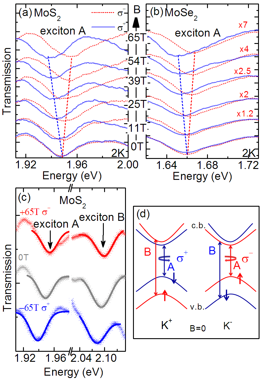
Representative low temperature magneto-transmission spectra obtained for a single layer MoS2 and MoSe2 showing A-exciton absorption are presented in Fig. 1(a-b) for and circular polarization. For MoSe2 each spectra in magnetic field has been multiplied by a suitable numerical factor to have a similar absorption intensity as the spectra. The minima observed in all the spectra occurs at an energy corresponding to the expected A-exciton absorption in both materials.Wang et al. (2012)
A clear splitting of both exciton transitions is observed which increases linearly with increasing the magnetic field and reaches about 18 meV at the maximum applied field (65 T). Such a splitting has been previously observed in PL measurements at lower magnetic field in exfoliated samples. Li et al. (2014); MacNeill et al. (2015); Srivastava et al. (2015); Aivazian et al. (2015); Wang et al. (2012); Mitioglu et al. (2015) The valley splitting arises from the opposite sign of the valley magnetic moment in the valence band. The relative magnetic field induced energy shift of the valence and conduction band in each valley is schematically presented in Fig. 1(d). The dipole-allowed transitions for the A and B-excitons are indicated by the vertical arrows. For both excitons polarized light couples to the valley while polarized light couples to the valley. In the absence of a magnetic field, the transitions have identical energies for both the A and B-excitons. Applying a magnetic field breaks the time-reversal symmetry, lifting the valley degeneracy, which splits the () transitions. It is important to note that the schematic in the Fig. 1(d) is valid only for molybdenum dichalcogenides. For the tungsten dichalcogenides, the order of the spin up/down conduction bands is reversed.Korm nyos et al. (2015).
| T(K) | MoS2 A | MoS2 B | MoSe2 A |
|---|---|---|---|
| 2 | |||
| 77 | |||
| 120 |
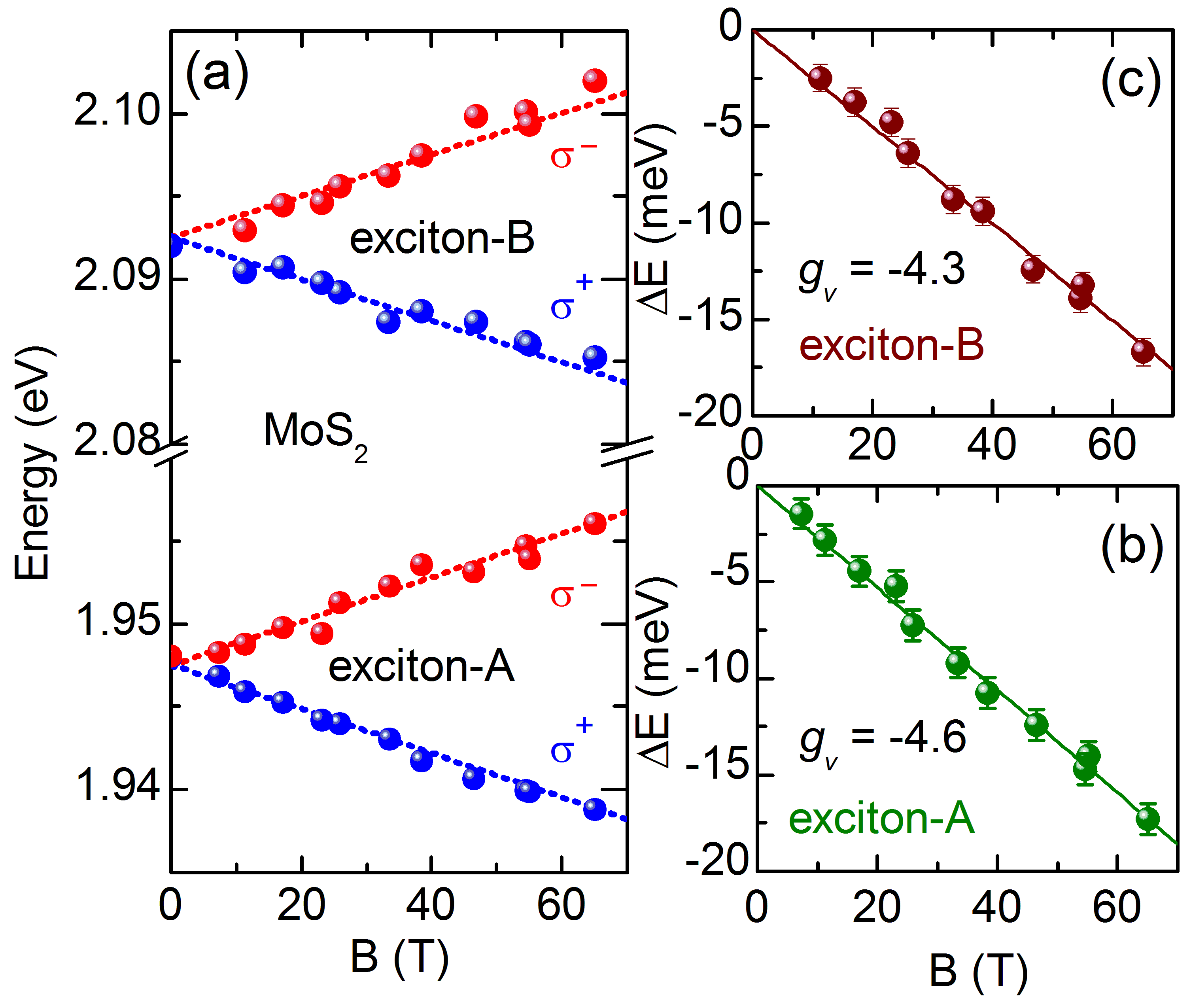
To extract the exciton splitting energy at each magnetic field, the energy of the absorption line was determined by fitting a Gaussian function. Examples of the fitted spectra at and T for both circular polarizations are shown in Fig. 1(c). The spectra are shown for MoS2 in the energy range covering both the A and B excitons. The energy of the A and B-excitonic transitions as a function of magnetic field in monolayer MoS2 is plotted in Fig. 2(a) for polarizations. For both excitons, the energy of the transitions evolve linearly with magnetic field.
The difference between the transition energy with and circular polarized light () in magnetic field for both excitons is presented in Fig. 2(b-c). The exciton valley splitting scales linearly with the magnetic field and is almost identical for both excitons. A linear fit to the data gives and for the A and B-excitons respectively. Similar values for the exciton A were reported for exfoliated monolayer MoSe2 samples using photoluminescence measurements in low magnetic fields. Li et al. (2014); MacNeill et al. (2015) The expected evolution of the transition energies in magnetic field, calculated using the valley Zeeman splitting is indicated in Fig. 2(a) by the broken lines. The excellent agreement with the data confirms that within experimental error the splitting is symmetric with no evidence for a diamagnetic shift or cyclotron-like free carrier contribution to the magnetic field evolution of the transitions.
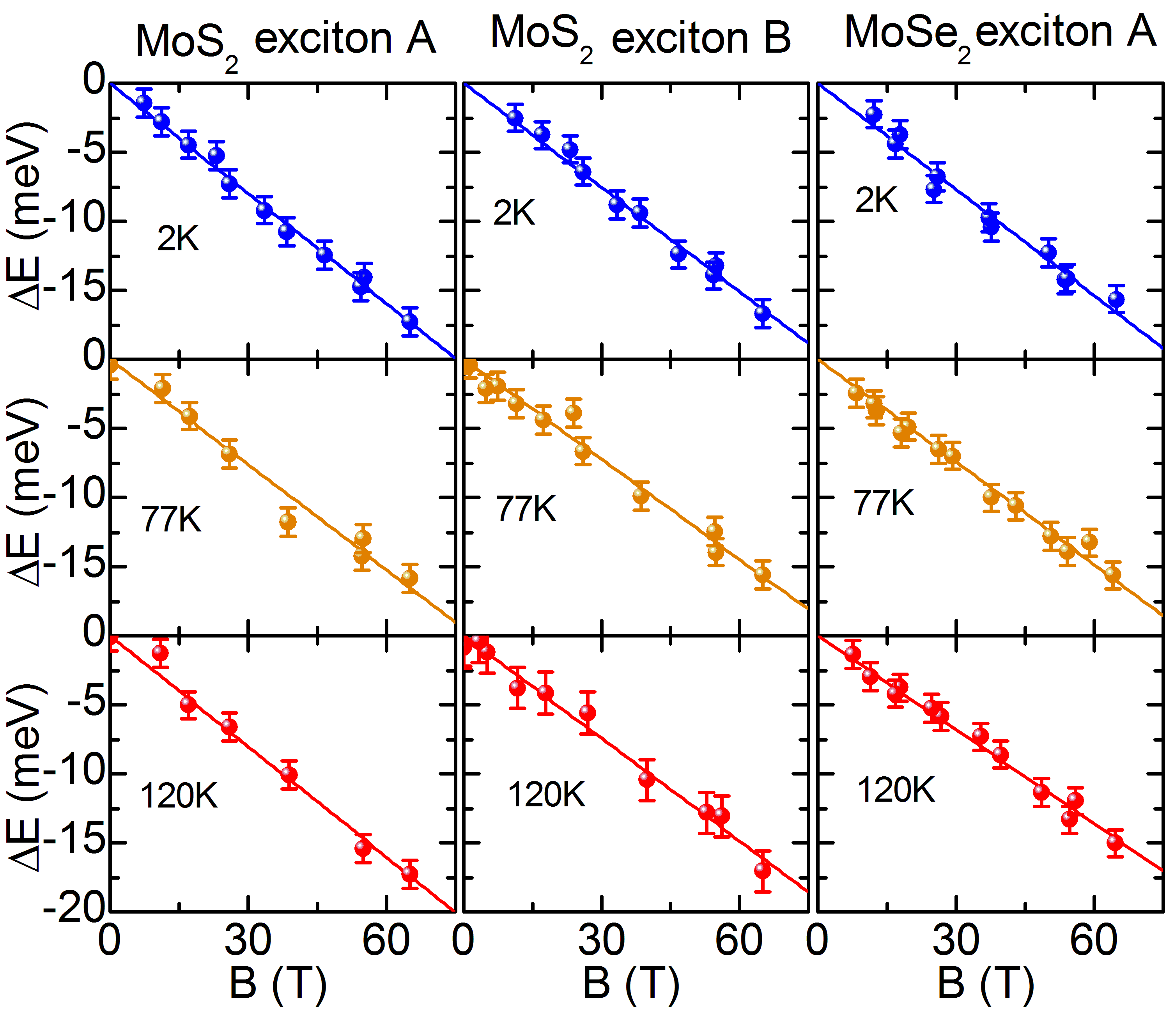
We have measured transmission spectra at and T () for three different temperatures for the A and B-excitons in MoS2 and A-exciton in MoSe2 (exciton B is not resolved in our CVD MoSe2 samples). The precise position of the exciton transitions as a function of magnetic field was obtained by fitting Gaussian functions. The obtained splitting between the and transitions is plotted in Fig. 3 versus the magnetic field at three different temperatures. The valley g-factors were extracted by linear fits to the data (solid lines). The values of the temperature dependent valley g-factor are summarized in Table 1. In MoS2, for both excitonic transitions the valley g factor is independent of the temperature within experimental error. For MoSe2, where only the exciton A is observed, the g-factor is constant within experimental error for K and decreases by around 10% at K.
III.2 The influence of strain
Strain modifies the ratio of the effective masses in the valence and the conduction bands giving rise to an intercellular contribution to the valley splitting which then takes the form , where and are the effective masses in the conduction and valence band in the units of the free electron mass. Liu et al. (2013); Aivazian et al. (2015) In principle can be calculated taking into account higher order corrections to the tight binding model. Estimations vary between to depending if only nearest neighbor (NN) or next nearest neighbor (NNN) hopping parameters are taken into account in three band tight binding model Liu et al. (2013); Aivazian et al. (2015). CVD grown samples, are naturally strainedDumcenco et al. (2015); Liu et al. (2014), which results in the modification of the band structure, in particular the ratio of the effective masses in the valence and conduction bandsConley et al. (2013); Yue et al. (2012); Scalise et al. (2014); Rostami et al. (2015).
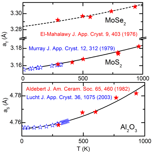
To estimate the strain we need to know the temperature dependence of the lattice constant of the bulk TMDs and sapphire from the lowest measurement temperature up to the growth temperature (C K) at which the TMD monolayer is assumed to be unstrained. In Fig. 4 we plot the lattice constant assembling published data in the literatureAlderbert and Traverse (1982); El-Mahalawy and Evans (1976); Lucht et al. (2003); Murray and Evans (1979) in order to span the temperature range of interest for MoS2, MoSe2 and sapphire. The solid lines are second order polynomial fits which we use to calculate the strain versus temperature. For MoSe2 we were unable to find any published data below room temperature. Fortunately, the high temperature data suggests that the temperature dependence of MoS2 and MoSe2 are almost identical. We therefore use the fitted temperature dependence of MoS2 which has been shifted vertically (broken line).
The strain is by definition,
where is the lattice constant of the TMD grown on sapphire and is the lattice constant of the unstrained bulk TMD. Assuming that the TMD monolayer is constrained to follow the thermal contraction of the sapphire substrate when the sample is cooled from the growth temperature we can write,
where is the lattice constant of the sapphire substrate. Thus, the strain is given by,
which can be calculated using the polynomial approximations for the evolution of the lattice constants with temperature.
The calculated strain for MoS2 and MoSe2 is plotted in Fig. 5(a). For both TMDs the strain remains negligibly small as the sample is cooled from the growth temperature to K. Below this temperature the tensile strain progressively increases reaching 0.2% in MoS2 at low temperature. For MoSe2 the strain is slightly smaller reaching a maximum value of % at K.
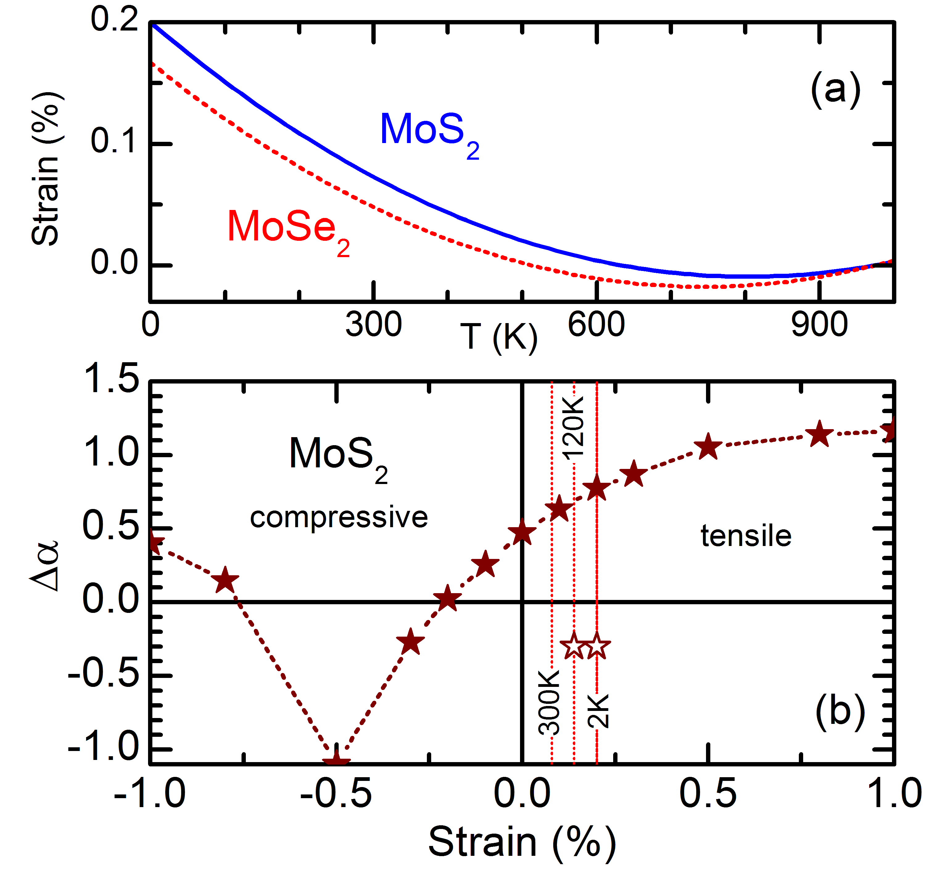
In order to estimate the intercellular correction to the valley magnetic moment we have calculated using the electron and hole effective masses at the -point in MoS2, calculated as a function of strain, using density-functional theory (DFT).Scalise et al. (2014) The result is plotted as closed symbols in Fig. 5(b). The vertical broken lines indicate the expected strain in MoS2 at K, K and room temperature. While varies little over the range of strain of interest, in line with the observation that the valley g-factor remains almost unchanged with temperature, the value of , notably its sign, is not in agreement with the measured g-factors with which implies that should be negative. The open symbols indicated the required values of to have agreement with the experimental valley g-factors. The failure of the DFT calculations to correctly predict the intercellular correction is not unexpected as excitons in TMDs are highly localized in real space, and thus delocalized in -space. This can in principle be taken into account by averaging the electron and hole effective masses over momentum space in the vicinity of the -points, which leads to a negative value of in agreement with experiment.Srivastava et al. (2015) However, such calculations are beyond the scope of this work.
Finally, the negligible influence of strain in CVD grown TMDs, is confirmed by the temperature dependence of the A-exciton absorption in MoS2 plotted in Fig. 6. We use the single oscillator model of O’Donnell and Chen to model the temperature dependence of the band gap.O’Donnell and Chen (1991) The solid line is a fit to the data using
where meV is the average phonon energy, is a dimensional coupling constant and eV is the low temperature band gap minus the exciton binding energy. The fit is excellent suggesting that strain plays little role in the observed temperature dependence. The expected variation of the band gap due to the change in strain with temperature, calculated from the measured meV/% strain red shift in monolayer MoS2,He et al. (2013) is shown by the dashed line in Fig. 6. Clearly the expected strain-induced meV change in the band gap is small compared to the observed meV change with temperature.
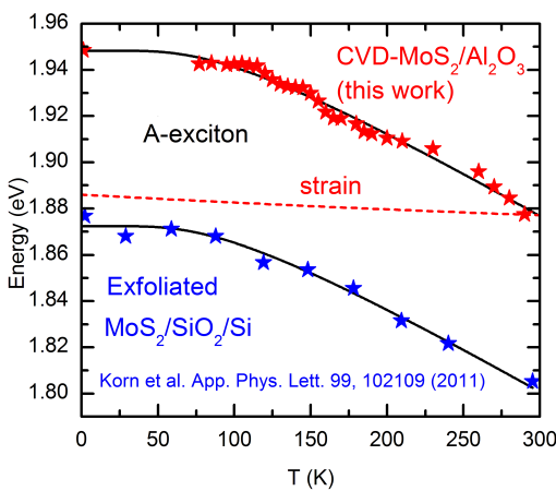
For comparison, we plot the energy of the A-exciton emission in exfoliated MoS2 on a SiO2/Si substrate taken from the literature.Korn et al. (2011) The energy of the emission is systematically shifted by meV due to the different dielectric environment (exciton binding energy). The solid line through the data is calculated using the same parameters as for the CVD MoS2 except for eV which is shifted due to the increased exciton binding energy. The excellent agreement with experiment demonstrates that exfoliated and CVD MoS2 have the same temperature dependence of the band gap, further confirming the negligible role played by strain in the latter.
IV Conclusion
We have investigated large-area monolayer MoS2 and MoSe2 samples, grown by CVD on sapphire, in high magnetic fields using optical absorption spectroscopy. The exciton valley splitting scales linearly with the magnetic field. In MoS2 the extracted low temperature ( K) valley g-factors are for the A-exciton and for the B-exciton. In MoSe2 for which only the A-exciton was observed we find at low temperatures. In both TMDs the g-factor is almost independent of temperature over the available measurement range (2-120 K). The strain present at low temperature % in our CVD grown TMDs has little effect on the electronic properties. The low temperature valley g-factors and the temperature dependence of the gap are identical to unstrained exfoliated MoS2 on SiO2/Si substrates. This suggests that the % tensile strain, which is naturally present in large area CVD grown Mo based TMDs on sapphire, does not represent any serious impediment for device applications.
During preparation of the manuscript, we became aware of similar work on CVD grown WS2 and MoS2 monolayers by the NHMFL-Los Alamos group. Stier et al. (2015)
Acknowledgements.
This work was partially supported by ANR JCJC project milliPICS, the Region Midi-Pyrénées under contract MESR 13053031, STCU project 5809 and the Swiss SNF Sinergia Grant no. 147607.References
- Wang et al. (2012) Q. H. Wang, K. Kalantar-Zadeh, A. Kis, J. N. Coleman, and M. S. Strano, Nature Nanotechnology 7, 699 (2012).
- Mak et al. (2010) K. F. Mak, C. Lee, J. Hone, J. Shan, and T. F. Heinz, Phys. Rev. Lett. 105, 136805 (2010).
- Splendiani et al. (2010) A. Splendiani, L. Sun, Y. Zhang, T. Li, J. Kim, C.-Y. Chim, G. Galli, and F. Wang, Nano Letters 10, 1271 (2010), pMID: 20229981.
- Xiao et al. (2012) D. Xiao, G.-B. Liu, W. Feng, X. Xu, and W. Yao, Phys. Rev. Lett. 108, 196802 (2012).
- Cao et al. (2012) T. Cao, G. Wang, W. Han, H. Ye, C. Zhu, J. Shi, Q. Niu, P. Tan, E. W. B. Liu, and J. Feng, Nature Communications 3, 887 (2012).
- Mak et al. (2012) K. F. Mak, K. He, J. Shan, and T. F. Heinz, Nature Nanotechnology 7, 494 (2012).
- Zeng et al. (2012) H. Zeng, J. Dai, W. Yao, D. Xiao, and X. Cui, Nature Nanotech. 7, 490 (2012).
- Sallen et al. (2012) G. Sallen, L. Bouet, X. Marie, G. Wang, C. R. Zhu, W. P. Han, Y. Lu, P. H. Tan, T. Amand, B. L. Liu, and B. Urbaszek, Phys. Rev. B 86, 081301 (2012).
- Jones et al. (2013) A. M. Jones, H. Yu, N. J. Ghimire, S. Wu, G. Aivazian, J. S. Ross, J. Yan, D. G. Mandrus, D. Xiao, W. Yao, and X. Xu, Nature Nanotech. 8, 634 (2013).
- Wu et al. (2013) S. Wu, J. S. Ross, G.-B. Liu, G. Aivazian, A. Jones, Z. Fei, W. Zhu, D. Xiao, W. Yao, D. Cobden, and X. Xu, Nature Physics 9, 149 (2013).
- Xu et al. (2014) X. Xu, W. Yao, D. Xiao, and T. F. Heinz, Nature Physics 10, 343 (2014).
- Mak et al. (2014) K. F. Mak, K. L. McGill, J. Park, and P. L. McEuen, Science 344, 1489 (2014).
- Yao et al. (2008) W. Yao, D. Xiao, and Q. Niu, Phys. Rev. B 77, 235406 (2008).
- Zhu et al. (2011) Z. Y. Zhu, Y. C. Cheng, and U. Schwingenschlögl, Phys. Rev. B 84, 153402 (2011).
- Rose et al. (2013) F. Rose, M. O. Goerbig, and F. Piéchon, Phys. Rev. B 88, 125438 (2013).
- Cai et al. (2013) T. Cai, S. A. Yang, X. Li, F. Zhang, J. Shi, W. Yao, and Q. Niu, Phys. Rev. B 88, 115140 (2013).
- Kormányos et al. (2014) A. Kormányos, V. Zólyomi, N. D. Drummond, and G. Burkard, Phys. Rev. X 4, 011034 (2014).
- Ho et al. (2014) Y.-H. Ho, Y.-H. Wang, and H.-Y. Chen, Phys. Rev. B 89, 155316 (2014).
- Chu et al. (2014) R.-L. Chu, X. Li, S. Wu, Q. Niu, W. Yao, X. Xu, and C. Zhang, Phys. Rev. B 90, 045427 (2014).
- Mitioglu et al. (2015) A. A. Mitioglu, P. Plochocka, A. G. del Aguila, P. C. M. Christianen, G. Deligeorgis, S. Anghel, L. Kulyuk, and D. K. Maude, Nano Letters 15, 4387 (2015), pMID: 26065723.
- Liu et al. (2013) G.-B. Liu, W.-Y. Shan, Y. Yao, W. Yao, and D. Xiao, Phys. Rev. B 88, 085433 (2013).
- MacNeill et al. (2015) D. MacNeill, C. Heikes, K. F. Mak, Z. Anderson, A. Kormányos, V. Zólyomi, J. Park, and D. C. Ralph, Phys. Rev. Lett. 114, 037401 (2015).
- Li et al. (2014) Y. Li, J. Ludwig, T. Low, A. Chernikov, X. Cui, G. Arefe, Y. D. Kim, A. M. van der Zande, A. Rigosi, H. M. Hill, S. H. Kim, J. Hone, Z. Li, D. Smirnov, and T. F. Heinz, Phys. Rev. Lett. 113, 266804 (2014).
- Srivastava et al. (2015) A. Srivastava, M. Sidler, A. V. Allain, D. S. Lembke, A. Kis, and A. Imamoglu, Nature Physics (2015), 10.1038/nphys3203.
- Aivazian et al. (2015) G. Aivazian, Z. Gong, A. M. Jones, R.-L. Chu, J. Yan, D. G. Mandrus, C. Zhang, D. Cobden, W. Yao, and X. Xu, Nature Physics 11, 148 (2015), arXiv:1407.2645 [cond-mat.mes-hall] .
- Wang et al. (2015) G. Wang, L. Bouet, M. M. Glazov, T. .Amand, E. L. Ivchenko, E. Palleau, X. Marie, and B. Urbaszek, 2D Materials 2, 034002 (2015).
- Rostami et al. (2015) H. Rostami, R. Roldán, E. Cappelluti, R. Asgari, and F. Guinea, Phys. Rev. B 92, 195402 (2015).
- Scalise et al. (2014) E. Scalise, M. Houssa, G. Pourtois, V. Afanasev, and A. Stesmans, Physica E: Low-dimensional Systems and Nanostructures 56, 416 (2014).
- Ramasubramaniam (2012) A. Ramasubramaniam, Phys. Rev. B 86, 115409 (2012).
- Dumcenco et al. (2015) D. Dumcenco, D. Ovchinnikov, K. Marinov, P. Lazic, M. Gibertini, N. Marzari, O. L. Sanchez, Y.-C. Kung, D. Krasnozhon, M.-W. Chen, S. Bertolazzi, P. Gillet, A. F. i Morral, A. Radenovic, and A. Kis, ACS Nano 9, 4611 (2015).
- Liu et al. (2014) Z. Liu, M. Amani, S. Najmaei, Q. Xu, X. Zou, W. Zhou, T. Yu, C. Qiu, A. G. Birdwell, F. J. Crowne, R. Vajtai, B. I. Yakobson, Z. Xia, M. Dubey, P. M. Ajayan, and J. Lou, NATURE COMMUNICATIONS 5 (2014), 10.1038/ncomms6246.
- Korm nyos et al. (2015) A. Korm nyos, G. Burkard, M. Gmitra, J. Fabian, V. Z lyomi, N. D. Drummond, and V. Fal ko, 2D Materials 2, 022001 (2015).
- Conley et al. (2013) H. J. Conley, B. Wang, J. I. Ziegler, R. F. Haglund, S. T. Pantelides, and K. I. Bolotin, Nano Letters 13, 3626 (2013).
- Yue et al. (2012) Q. Yue, J. Kang, Z. Shao, X. Zhang, S. Chang, G. Wang, S. Qin, and J. Li, Physics Letters A 376, 1166 (2012).
- Alderbert and Traverse (1982) P. Alderbert and J. P. Traverse, J. Am. Ceram. Soc. 65, 460 (1982).
- El-Mahalawy and Evans (1976) S. H. El-Mahalawy and B. L. Evans, Journal of Applied Crystallography 9, 403 (1976).
- Lucht et al. (2003) M. Lucht, M. Lerche, H.-C. Wille, Y. V. Shvyd’ko, H. D. Rüter, E. Gerdau, and P. Becker, Journal of Applied Crystallography 36, 1075 (2003).
- Murray and Evans (1979) R. Murray and B. Evans, Journal of Applied Crystallography 12, 312 (1979).
- O’Donnell and Chen (1991) K. P. O’Donnell and X. Chen, Applied Physics Letters 58, 2924 (1991).
- He et al. (2013) K. He, C. Poole, K. F. Mak, and J. Shan, Nano Letters 13, 2931 (2013), pMID: 23675872, http://dx.doi.org/10.1021/nl4013166 .
- Korn et al. (2011) T. Korn, S. Heydrich, M. Hirmer, J. Schmutzler, and C. Schüller, Applied Physics Letters 99, 102109 (2011).
- Stier et al. (2015) A. V. Stier, K. M. McCreary, B. T. Jonker, J. Kono, and S. A. Croocker, ArXiv e-prints (2015), arXiv:1510.07022 [cond-mat.mtrl-sci] .