1
Deterministic Single-Phonon Source Triggered by a Single Photon
Abstract
We propose a scheme that enables the deterministic generation of single phonons at GHz frequencies triggered by single photons in the near infrared. This process is mediated by a quantum dot embedded on-chip in an opto-mechanical circuit, which allows for the simultaneous control of the relevant photonic and phononic frequencies. We devise new opto-mechanical circuit elements that constitute the necessary building blocks for the proposed scheme and are readily implementable within the current state-of-the-art of nano-fabrication. This will open new avenues for implementing quantum functionalities based on phonons as an on-chip quantum bus.
Engineering of periodic nanostructures has proven to be an immensely powerful tool to shape the properties of a material. Most notably are photonic crystals, which are created by the periodic modulation of the refractive index. Their photonic bandgaps and defect modes have been widely studied Joannopoulos et al. (2011) and have found a number of applications in nano-photonics. For example, in solid-state quantum optics, they are commonly used to control light–matter interaction Lodahl et al. (2015). Similarly, the periodic modulation of mechanical properties leads to the formation of phononic crystals Gorishnyy et al. (2005). Chip-scale devices that allow engineering of both the photonic and the phononic density of states simultaneously have recently been proposed Maldovan and Thomas (2006); Eichenfield et al. (2009); Safavi-Naeini and Painter (2010); Mohammadi et al. (2010). This has lead to a range of theoretical Safavi-Naeini and Painter (2011); Galland et al. (2014); Schmidt et al. (2015) and experimental Chan et al. (2011); Cohen et al. (2015); Riedinger et al. (2016) breakthroughs in opto-mechanics. In parallel there has been significant progress on coupling single solid-state emitters, in the form of nitrogen-vacancy centers or self assembled quantum dots(QDs), to mechanical resonators either via magnetic gradient coupling Rabl et al. (2009); Arcizet et al. (2011) or strain coupling Wilson-Rae et al. (2004); Bennett et al. (2013); Ovartchaiyapong et al. (2014); Barfuss et al. (2015); MacQuarrie et al. (2013); Yeo et al. (2013); Montinaro et al. (2014). Additionally, the potential of using phononic crystals to control single-phonon mediated processes in solid-state systems has recently been alluded to Colless et al. (2014); Jahnke et al. (2015).
In optics, the reliable generation and detection of single-photon and entangled-photon states has important applications within quantum information science. Similar goals are being pursued in opto-mechanics where the generation Galland et al. (2014); Flayac and Savona (2014); Riedinger et al. (2016) and detection Cohen et al. (2015) of non-classical phononic states are opening new avenues of research. These schemes are typically probabilistic and rely on the direct radiation-pressure interaction between co-localized optical and mechanical modes where the coupling rate between the modes is proportional to the square root of the intra-cavity photon number Aspelmeyer et al. (2014). However, parasitic absorption is a problem for large intra-cavity photon numbers when operating at milikelvin temperatures Meenehan et al. (2014); Riedinger et al. (2016), which becomes necessary when performing experiments on single phonons with frequencies in the few GHz regime. In this paper we propose an alternative approach based on a hybrid opto-mechanical(OM)-crystal where we engineer the coupling of a three-level emitter to both the photonic and the phononic reservoirs. We demonstrate how the internal spin state of the emitter can be used to mediate strong photon-phonon interaction for an emitter embedded in the OM-crystal. In contrast to the standard approach in opto-mechanics Galland et al. (2014); Flayac and Savona (2014); Cohen et al. (2015); Aspelmeyer et al. (2014), our proposal does not rely on radiation-pressure coupling, which is strong for large intra-cavity photon numbers. Instead the deterministic single-photon–single-phonon cascade triggered by a single narrow-bandwidth photon is operated at an average intra-cavity photon numbers significantly below one 111We refer to Ref. Söllner et al. (2015) for a discussion about what constitutes narrow bandwidth for the incident photon and the role of dephasing in the coherent scattering regime., thus offering a route to circumvent the problem of parasitic heating. We propose a readily implementable device that can be used with QD emitters.
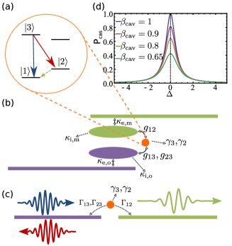
Our protocol is based on the two optical transitions of a lambda-system, given by a singly-charged QD (trion) in an in-plane magnetic field (Voigt-configuration), c.f. Fig. 1(a). In this configuration there are two allowed linearly-polarized optical transitions that decay at the same rate Press et al. (2008), while the two optical ground states are coupled by a spin-flip rate. Experiments have shown that it is possible to operate in a regime (depending on the Zeeman-splitting, sample temperature, and the co-tunnelling rates) where the spin-flip process is dominated by single-acoustic-phonon mediated transitions Kroutvar et al. (2004); Dreiser et al. (2008), which is in good agreement with theoretical predictions Khaetskii and Nazarov (2001); Woods et al. (2002); Golovach et al. (2004). We note that the coherence properties of the emitted phonons are inherited from the coherence of the spin. In many QD experiments the spin coherence is not limited by phonon mediated relaxation processes Warburton (2013), leading to emission of incoherent phonons. However, recently progress has been made towards increasing the spin-coherence times Prechtel et al. (2015) and the ultimately limiting process remains to be determined, especially when operating at mK-temperatures. The emitter is embedded in an OM-circuit shown schematically in Fig. 1(b). A photonic (phononic) waveguide couples the single photons (phonons) in-to and out-of the OM-circuit. The photonic and phononic waveguides each couple to their respective mode of the OM-cavity at the rates denoted and . All relevant rates are indicated in Fig. 1(b) and controlling their relative magnitudes offer a wide range of design possibilities. For the remainder of this paper we will focus on just one of these different realizations, which is well suited for the deterministic generation of single phonons. We consider the case where both cavity modes are in the over-coupled regime, meaning that the resonator loss is dominated by the coupling to the waveguide mode, ()() Galland et al. (2014). Thus the intrinsic cavity loss rates, and , can be neglected in the following. The emitter–resonator coupling is in the bad cavity but large cooperativity regime, i.e., and but and Rice and Carmichael (1988). In the bad cavity regime the influence of the cavity on an emitter close to resonance can be captured by a cavity-enhanced effective decay rate of the excited state into the cavity mode: , , and Rice and Carmichael (1988). Thus the schematic in Fig. 1(b) simplifies to the effective circuit shown in Fig. 1(c) for the implementation we are considering here. This is best described as an emitter coupled to unidirectional photonic and phononic reservoirs Rephaeli and Fan (2013); Ralph et al. (2015). The single-frequency scattering coefficient for the elastic scattering of a trigger photon, , incident on the transition is given by
| (1) |
For the case of and , i.e., when the two optical transitions are enhanced by the same amount and the incident photon is on resonance and is narrow-band compared to the QD transition, we see complete destructive interference of the scattered light at the resonance frequency . Thus, the photon has to be scattered along one of the remaining available decay channels Bradford et al. (2012); Shomroni et al. (2014). Consequently, the scattering coefficient for a trigger photon incident on the transition to Raman-scatter along the transition is,
| (2) |
From Eq.( 2) we calculate the success probability of initializing the single photon – single phonon cascade process, c.f. Fig. 1(d), which approaches unity for large coupling-efficiencies of the optical transitions. It is promising to note that recent experiments in photonic-crystal waveguides have shown that even for moderate enhancements of the waveguide mode, spontaneous-emission coupling-efficiencies can be readily achieved Arcari et al. (2014). This is largely the result of the strongly suppressed coupling to optical loss modes for QDs embedded in photonic-crystal membranes Wang et al. (2011). The incident and outgoing wavepackets for the successful generation of a photon–phonon cascade from a single incident trigger photon is illustrated in Fig. 1(c).
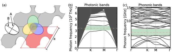
Implementing the circuit in Fig. 1(b) requires an OM-crystal that supports photonic and phononic band gaps at frequencies relevant to the optical transitions Lodahl et al. (2015) and the Zeeman-splitting Warburton (2013) obtainable for the considered emitter, i.e., InGaAs QDs. The OM-crystal we propose (shown in Fig. 2(a)) consists of a hexagonal array of holes, separated by the lattice constant etched into a GaAs membrane of thickness d=0.65a. Each hole is made up by three overlapping ellipses rotated by with respect to one another. The minor and major axes of the ellipse are given by A=0.45a and B=0.6a, respectively. The center of each ellipse is shifted outwards along its major axis by L=0.17a resulting in a final shape that is reminiscent of a shamrock, c.f. Fig. 2(a). This leads to a reduction of the crystal symmetry compared to conventional photonic Lodahl et al. (2015) and previous OM-crystals Safavi-Naeini and Painter (2010) (c.f. the Supplementary Material (SM) for more information 222See Supplemental Material at [URL will be inserted by publisher] for more information on the reduction of the crystal symmetry.). A similar structure has been investigate for its photonic properties Wen et al. (2008).
The photonic band-diagram for modes with TE-like symmetry is shown in Fig. 2(b). The lightly shaded region in the center indicates the in-plane band-gap and the dashed line marks the position of the optical transitions within the band-gap. The dark shaded region at the sides and the top of Fig. 2(b) indicates the continuum of leaky radiation modes, i.e., modes that are not confined to the membrane. For simulations of the phononic bands (see SM for details) we consider the modes of all symmetries, c.f. Fig. 2(c), taking into account the anisotropy of the elastic constants of gallium arsenide. In the phononic band structure there are no leaky modes, as all modes are confined to the membrane. Thus, contrary to the photonic case, the phononic band-diagrams exhibit a complete band-gap. This has promising implications for the control of single-phonon mediated transitions as they can be completely suppressed within the band-gap, where the phononic density of states drops to zero. For our proposal this means that the coupling efficiency of the transition to the phononic cavity mode is only limited by the probability to decay through a single-phonon process, as opposed to other spin-relaxation processes such as co-tunneling Dreiser et al. (2008) and multi-phonon effects Khaetskii and Nazarov (2001); Woods et al. (2002); Trif et al. (2009). This differs from the coupling efficiencies in photonic systems, where in addition to the probability of the emitter decaying through a single photon process, the coupling efficiency is limited by the coupling to non-guided radiation modes Arcari et al. (2014). Nonetheless, completely analogous to optical emitters in photonic crystals, the coupling rate to the target mode can be enhanced by increasing the local density of mechanical states through the use of defect modes.
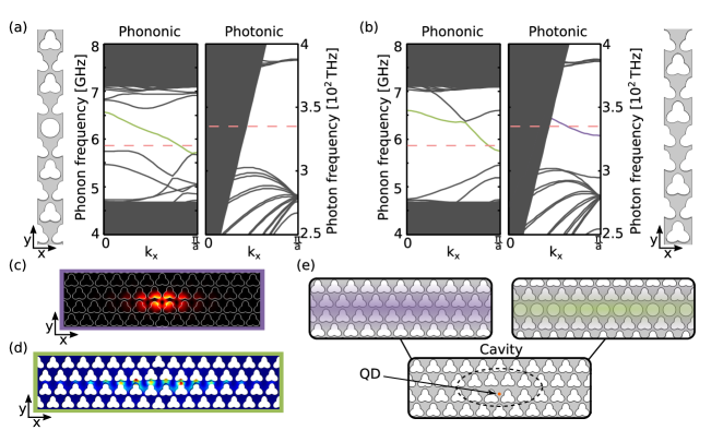
We now demonstrate some of the different types of defect modes employed for the realization of the proposal. In Fig. 3(a) we show a phononic waveguide formed by replacing a row of shamrock holes by circular holes. This waveguide exhibits a gap at the relevant photonic frequencies, and corresponds to the waveguide at the top of Fig. 1(b). It allows introducing a large , by bringing it close to the cavity, while leaving the optical cavity modes largely unaffected. A different waveguide design is obtained by removing a row of shamrock holes and scaling the spacing between the remaining adjacent rows of holes to . The modes for a waveguide width of W=0.58 are shown in Fig.3(b). This waveguide supports both a photonic and a phononic mode with band edges close to the respective transition frequencies of the emitter. The band edges of both modes shift up in frequency when reducing the width of the waveguide, eventually, leading to a dual band gap at the frequencies relevant for the emitter for W=0.52. This makes the waveguide in Fig.3(b) well suited for the design of hetero-structure cavities, that simultaneously support modes at the desired photonic and phononic frequencies Safavi-Naeini and Painter (2010, 2011), which corresponds to the OM-cavity drawn in Fig. 1(b). One realization of such a cavity and the mode-profiles of the optical and the mechanical modes are shown in Fig. 3(c) and (d). In Fig. 3(e) the circuit elements needed to assemble the circuit sketched in Fig. 1(b) are collected. The two types of waveguides discussed suffice to realize the OM-circuit sketched in Fig. 1(b) and (c) by ensuring that the cavities dominant mechanical loss rate, , is to the phononic waveguide in Fig. 3(a). However, similar design ideas have been used to realize photonic waveguide defects in the same OM-crystal (not shown). Thus, this new type of OM-crystal is a versatile platform for on-chip opto-mechanics.
In this work we have demonstrated a scheme for single-phonon generation in an opto-mechanical crystal. The scheme is based on QD embedded in a membrane GaAs nanostructure whose periodic properties lead to simultaneous photonic and phononic band-gaps, allowing to control optical and acoustical interaction processes in the emitter. We have designed waveguides and cavities for both photons and phonons by introducing different types of crystal defects. Throughout the work the focus has been on designing structures that can be experimentally realized within the current scope of gallium arsenide nano-fabrication.
Finally we note that other solid-state systems, such as silicon-vacancy centers in diamond, appear to have spin-coherence times limited by single-phonon mediated relaxation processes Rogers et al. (2014); Pingault et al. (2014). In addition to enhancing the spin coherence of such a system it also becomes possible for the phonons to act as a coherent on-chip quantum-bus, which can couple several emitters Bennett et al. (2013) or act as a transducer from the optical to the microwave regime Davanço et al. (2012); Bochmann et al. (2013). When exploiting the type of three-level system discussed here the resulting photon–phonon cascade can be used to implement the DLCZ-protocol (Duan, Lukin, Cirac, and Zoller)Duan et al. (2001). Other possible applications include the creation of vibration amplification by stimulated emission of radiation Kepesidis et al. (2013).
We would like to thank Alisa Javadi, Anders Sørensen, Richard Warburton, Petru Tighineanu, Sahand Mahmoodian, and Tommaso Pregnolato for helpful discussions. We gratefully acknowledge financial support from the the Danish Council for Independent Research (Natural Sciences and Technology and Production Sciences) and the European Research Council (ERC Consolidator Grant - ALLQUANTUM).
References
- Joannopoulos et al. (2011) J. D. Joannopoulos, S. G. Johnson, J. N. Winn, and R. D. Meade, Photonic Crystals: Molding the Flow of Light, 2nd ed. (Princeton University Press, 2011).
- Lodahl et al. (2015) P. Lodahl, S. Mahmoodian, and S. Stobbe, Reviews of Modern Physics 87, 347 (2015).
- Gorishnyy et al. (2005) T. Gorishnyy, M. Maldovan, C. Ullal, and E. Thomas, Physics World 18, 24 (2005).
- Maldovan and Thomas (2006) M. Maldovan and E. L. Thomas, Applied Physics Letters 88, 251907 (2006).
- Eichenfield et al. (2009) M. Eichenfield, J. Chan, R. M. Camacho, K. J. Vahala, and O. Painter, Nature 462, 78 (2009).
- Safavi-Naeini and Painter (2010) A. H. Safavi-Naeini and O. Painter, Optics Express 18, 14926 (2010).
- Mohammadi et al. (2010) S. Mohammadi, A. A. Eftekhar, A. Khelif, and A. Adibi, Optics Express 18, 9164 (2010).
- Safavi-Naeini and Painter (2011) A. H. Safavi-Naeini and O. Painter, New Journal of Physics 13, 013017 (2011).
- Galland et al. (2014) C. Galland, N. Sangouard, N. Piro, N. Gisin, and T. J. Kippenberg, Physical Review Letters 112, 143602 (2014).
- Schmidt et al. (2015) M. Schmidt, V. Peano, and F. Marquardt, New Journal of Physics 17, 023025 (2015).
- Chan et al. (2011) J. Chan, T. P. M. Alegre, A. H. Safavi-Naeini, J. T. Hill, A. Krause, S. Groeblacher, M. Aspelmeyer, and O. Painter, Nature 478, 89 (2011).
- Cohen et al. (2015) J. D. Cohen, S. M. Meenehan, G. S. MacCabe, S. Gröblacher, A. H. Safavi-Naeini, F. Marsili, M. D. Shaw, and O. Painter, Nature 520, 522 (2015).
- Riedinger et al. (2016) R. Riedinger, S. Hong, R. A. Norte, J. A. Slater, J. Shang, A. G. Krause, V. Anant, M. Aspelmeyer, and S. Gröblacher, Nature (2016), 10.1038/nature16536.
- Rabl et al. (2009) P. Rabl, P. Cappellaro, M. V. Gurudev Dutt, L. Jiang, J. R. Maze, and M. D. Lukin, Physical Review B 79, 041302 (2009).
- Arcizet et al. (2011) O. Arcizet, V. Jacques, A. Siria, P. Poncharal, P. Vincent, and S. Seidelin, Nature Physics 7, 879 (2011).
- Wilson-Rae et al. (2004) I. Wilson-Rae, P. Zoller, and A. Imamoğlu, Physical Review Letters 92, 075507 (2004).
- Bennett et al. (2013) S. D. Bennett, N. Y. Yao, J. Otterbach, P. Zoller, P. Rabl, and M. D. Lukin, Physical Review Letters 110, 156402 (2013).
- Ovartchaiyapong et al. (2014) P. Ovartchaiyapong, K. W. Lee, B. A. Myers, and A. C. B. Jayich, Nature Communications 5, 4429 (2014).
- Barfuss et al. (2015) A. Barfuss, J. Teissier, E. Neu, A. Nunnenkamp, and P. Maletinsky, Nature Physics 11, 820 (2015).
- MacQuarrie et al. (2013) E. R. MacQuarrie, T. A. Gosavi, N. R. Jungwirth, S. A. Bhave, and G. D. Fuchs, Physical Review Letters 111, 227602 (2013).
- Yeo et al. (2013) I. Yeo, P.-L. de Assis, A. Gloppe, E. Dupont-Ferrier, P. Verlot, N. S. Malik, E. Dupuy, J. Claudon, J.-M. Gérard, A. Auffèves, G. Nogues, S. Seidelin, J.-P. Poizat, O. Arcizet, and M. Richard, Nature Nanotechnology 9, 106 (2013).
- Montinaro et al. (2014) M. Montinaro, G. Wüst, M. Munsch, Y. Fontana, E. Russo-Averchi, M. Heiss, A. Fontcuberta I Morral, R. J. Warburton, and M. Poggio, Nano Letters 14, 4454 (2014).
- Colless et al. (2014) J. I. Colless, X. G. Croot, T. M. Stace, A. C. Doherty, S. D. Barrett, H. Lu, A. C. Gossard, and D. J. Reilly, Nature Communications 5, 3716 (2014).
- Jahnke et al. (2015) K. D. Jahnke, A. Sipahigil, J. M. Binder, M. W. Doherty, M. Metsch, L. J. Rogers, N. B. Manson, M. D. Lukin, and F. Jelezko, New Journal of Physics 17, 043011 (2015).
- Flayac and Savona (2014) H. Flayac and V. Savona, Physical Review Letters 113, 143603 (2014).
- Aspelmeyer et al. (2014) M. Aspelmeyer, T. J. Kippenberg, and F. Marquardt, Reviews of Modern Physics 86, 1391 (2014).
- Meenehan et al. (2014) S. M. Meenehan, J. D. Cohen, S. Gröblacher, J. T. Hill, A. H. Safavi-Naeini, M. Aspelmeyer, and O. Painter, Physical Review A 90, 011803(R) (2014).
- Note (1) We refer to Ref. Söllner et al. (2015) for a discussion about what constitutes narrow bandwidth for the incident photon and the role of dephasing in the coherent scattering regime.
- Press et al. (2008) D. Press, T. D. Ladd, B. Zhang, and Y. Yamamoto, Nature 456, 218 (2008).
- Kroutvar et al. (2004) M. Kroutvar, Y. Ducommun, D. Heiss, M. Bichler, D. Schuh, G. Abstreiter, and J. J. Finley, Nature 432, 81 (2004).
- Dreiser et al. (2008) J. Dreiser, M. Atatüre, C. Galland, T. Müller, A. Badolato, and A. Imamoğlu, Physical Review B 77, 075317 (2008).
- Khaetskii and Nazarov (2001) A. V. Khaetskii and Y. V. Nazarov, Physical Review B 64, 125316 (2001).
- Woods et al. (2002) L. Woods, T. Reinecke, and Y. Lyanda-Geller, Physical Review B 66, 161318(R) (2002).
- Golovach et al. (2004) V. N. Golovach, A. Khaetskii, and D. Loss, Physical Review Letters 93, 016601 (2004).
- Warburton (2013) R. J. Warburton, Nature Materials 12, 483 (2013).
- Prechtel et al. (2015) J. H. Prechtel, A. V. Kuhlmann, J. Houel, A. Ludwig, S. R. Valentin, A. D. Wieck, and R. J. Warburton, Unpublished (2015).
- Rice and Carmichael (1988) P. R. Rice and H. J. Carmichael, IEEE Journal of Quantum Electronics 24, 1351 (1988).
- Rephaeli and Fan (2013) E. Rephaeli and S. Fan, Photonics Research 1, 110 (2013).
- Ralph et al. (2015) T. Ralph, I. Söllner, S. Mahmoodian, A. White, and P. Lodahl, Physical Review Letters 114, 173603 (2015).
- Bradford et al. (2012) M. Bradford, K. C. Obi, and J. T. Shen, Physical Review Letters 108, 103902 (2012).
- Shomroni et al. (2014) I. Shomroni, S. Rosenblum, Y. Lovsky, O. Bechler, G. Guendelman, and B. Dayan, Science 345, 903 (2014).
- Arcari et al. (2014) M. Arcari, I. Söllner, A. Javadi, S. L. Hansen, S. Mahmoodian, J. Liu, H. Thyrrestrup, E. H. Lee, J. D. Song, S. Stobbe, and P. Lodahl, Physical Review Letters 13, 093603 (2014).
- Wang et al. (2011) Q. Wang, S. Stobbe, and P. Lodahl, Physical Review Letters 107, 167404 (2011).
- Note (2) See Supplemental Material at [URL will be inserted by publisher] for more information on the reduction of the crystal symmetry.
- Wen et al. (2008) F. Wen, S. David, X. Checoury, M. El Kurdi, and P. Boucaud, Optics Express 16, 12278 (2008).
- Trif et al. (2009) M. Trif, P. Simon, and D. Loss, Physical Review Letters 103, 106601 (2009).
- Rogers et al. (2014) L. J. Rogers, K. D. Jahnke, M. H. Metsch, A. Sipahigil, J. M. Binder, T. Teraji, H. Sumiya, J. Isoya, M. D. Lukin, P. Hemmer, and F. Jelezko, Physical Review Letters 113, 263602 (2014).
- Pingault et al. (2014) B. Pingault, J. N. Becker, C. H. Schulte, C. Arend, C. Hepp, T. Godde, A. I. Tartakovskii, M. Markham, C. Becher, and M. Atatüre, Physical Review Letters 113, 263601 (2014).
- Davanço et al. (2012) M. Davanço, J. Chan, A. H. Safavi-Naeini, O. Painter, and K. Srinivasan, Optics Express 20, 24394 (2012).
- Bochmann et al. (2013) J. Bochmann, A. Vainsencher, D. D. Awschalom, and A. N. Cleland, Nature Physics 9, 712 (2013).
- Duan et al. (2001) L. M. Duan, M. D. Lukin, J. I. Cirac, and P. Zoller, Nature 414, 413 (2001).
- Kepesidis et al. (2013) K. V. Kepesidis, S. D. Bennett, S. Portolan, M. D. Lukin, and P. Rabl, Physical Review B 88, 064105 (2013).
- Söllner et al. (2015) I. Söllner, S. Mahmoodian, S. L. Hansen, L. Midolo, A. Javadi, G. Kiršanskė, T. Pregnolato, H. El-Ella, E. H. Lee, J. D. Song, S. Stobbe, and P. Lodahl, Nature Nanotechnology 10, 775 (2015).
I Supplementary Material for “Deterministic Single-Phonon Source Triggered by a Single Photon”
I.1 The Irreducible Brillouin Zone of the Shamrock-crystal
Most work to date on photonic-crystals uses circularly symmetric holes (), typically in a hexagonal lattice () Sakoda (2005), leading to a crystal that belongs to the planar space-group (also called wallpaper group) p6mm Mirman (1999). Recent studies investigating novel opto-mechanical crystals, known as snowflake-crystals Safavi-Naeini and Painter (2010), the symmetry of the hole has been reduced to match the symmetry of the lattice (). This again leads to a crystal that belongs to the planar space-group p6mm. However, for the shamrock-crystal, c.f. Fig. 4a), the symmetry of the hole is reduced further by removing three of the mirror planes which results in a symmetry of the hole. For the orientation of the hole with respect to the lattice shown in Fig. 4a) the total structure belongs to the planar space-group p3m1 Mirman (1999). The symmetries of the photonic and phononic modes are inherited from the symmetries of the structure as is the irreducible Brillouin zone (IRBZ), c.f. Fig. 4b)Terzibaschian and Enderlein (1986). In addition, the photonic and phononic modes must be eigenstates of the inversion operator, which is not one of the symmetry operators of the planar space-group p3m1. This arises because all modes fulfilling time-reversal symmetry must be eigenstates of the inversion operator. Since inversion was not a symmetry operator of the initial crystal structure this changes the IRBZ shown in Fig. 4b) to an effective IRBZ, Fig. 4c) Andreani and Gerace (2006); Wen et al. (2008). This is the IRBZ of a crystal that belongs to the standard planar space-group p6mm Terzibaschian and Enderlein (1986) and is used for all simulations presented in this work.
The photonic-bands were calculated using the freely available software package MIT Photonic Bands Johnson and Joannopoulos (2001). For the calculations of the photonic modes a refractive index of 3.48 is used, which corresponds to GaAs at . The photonic cavity modes were calculated in a commercially available finite-element solver. This software was also used for the calculation of the phononic-bands and the phononic cavity modes. The large degree of anisotropy in GaAs is taken into account in the phononic simulations, where we have used the three elastic constants relevant for GaAs 333Can be found at: http://www.ioffe.ru/SVA/NSM/Semicond/GaAs/mechanic.html..

References
- Sakoda (2005) K. Sakoda, Optical Properties of Photonic Crystals, 2nd ed., edited by W. Rhodes (Springer Berlin Heidelberg New York, 2005) p. 253.
- Mirman (1999) R. Mirman, Point Groups, Space Groups, Crystals, Molecules (World Scientific, 1999).
- Safavi-Naeini and Painter (2010) A. H. Safavi-Naeini and O. Painter, Optics Express 18, 14926 (2010).
- Terzibaschian and Enderlein (1986) T. Terzibaschian and R. Enderlein, Physica Status Solidi (B) 133, 443 (1986).
- Andreani and Gerace (2006) L. C. Andreani and D. Gerace, Physical Review B 73, 235114 (2006).
- Wen et al. (2008) F. Wen, S. David, X. Checoury, M. El Kurdi, and P. Boucaud, Optics Express 16, 12278 (2008).
- Johnson and Joannopoulos (2001) S. Johnson and J. Joannopoulos, Optics Express 8, 173 (2001).
- Note (3) Can be found at: http://www.ioffe.ru/SVA/NSM/Semicond/GaAs/mechanic.html.