The Role of Short-Range Order and Hyperuniformity in the Formation of Band Gaps in Disordered Photonic Materials
Abstract
We study photonic band gap formation in two-dimensional high refractive index disordered materials where the dielectric structure is derived from packing disks in real and reciprocal space. Numerical calculations of the photonic density of states demonstrate the presence of a band gap for all polarizations in both cases. We find that the band gap width is controlled by the increase in positional correlation inducing short-range order and hyperuniformity concurrently. Our findings suggest that the optimization of short-range order, in particular the tailoring of Bragg scattering at the isotropic Brillouin zone, are of key importance for designing disordered PBG materials.
pacs:
41.20.Jb, 42.70.Qs, 78.67.Pt, 61.43.-jPhotonic band gap (PBG) materials exhibit frequency bands where the propagation of light is strictly prohibited.
Such materials are usually designed by arranging high refractive index dielectric material on a crystal lattice Joannopoulos et al. (2008); López (2003).
The description of wave transport in a periodically repeating environment provides a clear physical mechanism for the emergence of PBGs, in analogy to common electronic semiconductors.
It is also known that certain aperiodic dielectric structures, such as quasicrystals Parker et al. (2000); Rechtsman et al. (2008); Edagawa (2014), can display a full PBG.
Over the last decade disordered or amorphous photonic materials have gained growing attention Jin et al. (2001); Rockstuhl et al. (2006); Shi et al. (2013); Rojas-Ochoa et al. (2004); Markoš and Soukoulis (2005); Reufer et al. (2007); Galisteo-López et al. (2011); Rechtsman et al. (2011); Izrailev et al. (2012); Wiersma (2013); Conley et al. (2014); Haberko and Scheffold (2013); Muller et al. (2014).
This trend is motivated by the many disordered photonic materials found in nature that reveal fascinating structural color effects in plants, insects, and mammals Sun et al. (2013).
At the same time, fabricating perfect crystalline structures with photonic properties at optical wavelengths has proven to be more difficult than initially anticipated Lourtioz (2004). It has been argued that disordered PBG materials should be less sensitive to fabrication errors or defects and thus promise a more robust design platform Wiersma (2013).
Moreover PBGs in disordered dielectrics are isotropic, which could make it easier to achieve a full PBG while at the same time offering better performance in wave guiding, design of non-iridescent stable pigments, and display applications Man et al. (2013); Takeoka (2012); Park et al. (2014); Dyachenko et al. (2014).
Yet, until recently, direct evidence for the existence of full PBGs in disordered photonic materials had been scarce and the fabrication principles and physical-optical mechanism leading to PBG formation remained obscure.
Although the importance of appropriate short-range order for the development of PBGs in disordered photonic materials was discovered early on Jin et al. (2001); Rockstuhl et al. (2006); Shi et al. (2013); Rojas-Ochoa et al. (2004), a strategy to maximize the PBG width was lacking.
In 2009 Florescu and coworkers Florescu et al. (2009) proposed a new approach for the design of disordered PBG materials that has attracted widespread attention. They introduced the concept of hyperuniformity for photonic structures, which enforces a certain type of short-range order. In particular, so-called stealthy hyperuniform (SHU) disordered patterns were reported to be fully transparent to incident long-wavelength radiation Batten et al. (2008); Leseur et al. (2015) and lead to strong isotropic PBGs at shorter wavelengths Florescu et al. (2009). Other types of correlated disorder, such as those generated by the random-sequential absorption model, were claimed to be inferior because they do not induce the formation of PBGs for both polarizations simultaneously Florescu et al. (2009). To the contrary, independent numerical work showed that the amorphous diamond structure Edagawa et al. (2008) and three-dimensional networks derived from systems of densely packed spheres Liew et al. (2011) exhibit a full PBG in the absence of stealthiness.
Here we aim to disentangle the role of short-range order and hyperuniformity in producing PBGs. To establish a comparison between different disordered systems, we compare, using otherwise identical design protocols matching those studied in Ref. Florescu et al. (2009), the photonic properties of systems with varying degrees and types of correlations: (i) collections of rods for transverse-magnetic (TM) polarization, (ii) trivalent networks (connected walls) for transverse-electric (TE) polarization, and (iii) decorated trivalent networks for both polarizations. Our results suggest that stealthy hyperuniformity and disk packing are equivalent strategies for the design of two-dimensional disordered photonic materials.
Pattern generation.—Hyperuniformity corresponds to the suppression of long-range density fluctuations and can be expressed as a condition for the structure factor, . Stealthiness is even more restrictive and requires the structure factor to vanish over a finite range, for Batten et al. (2008). Importantly, two-dimensional SHU patterns can be regarded as a reciprocal-space counterpart of packing hard disks (HDs) Torquato et al. (2015) of radius , which fulfill the condition for the radial distribution function. In both cases the excluded zone is determined by a dimensionless parameter, the packing fraction in real space and stealthiness in reciprocal space Batten et al. (2008). We interpret these parameters as measures for the amount of correlation in the system restricting randomness. Increasing or leads to pronounced peaks in and , indicating the development of short-range positional order. Upon further increase of or , entropy-driven crystallization sets in eventually. Moreover, hyperuniformity is recovered asymptotically, for , when disks are packed into a maximally jammed configuration via compression while avoiding crystallization Donev et al. (2005); Ikeda and Berthier (2015).
We generate disordered point patterns with different levels of positional correlation as measured by and using computer simulation Sup . Disordered HD patterns are equilibrated fluids. SHU patterns are obtained using a pair potential derived from the potential energy, , where the discreteness of the sum is a consequence of the periodic simulation box used. We employ a simulated annealing relaxation scheme to find disordered SHU patterns with for . Selecting an area in real space for a given number of points sets the number density and defines a characteristic length scale , comparable to a typical distance between the points.
The patterns calculated with our algorithms quantitatively reproduce previously reported Torquato et al. (2015) statistics and correlation functions. Patterns below the critical parameters , in which quasi-long-range order gradually appears Bernard and Krauth (2011); Engel et al. (2013); Torquato et al. (2015), already have significant short-range order. Fig. 1(a-f) shows representative HD and SHU point patterns at and , respectively. These parameter values were chosen as high as possible while retaining the amorphous structure and matching the peaks as closely as possible. A close similarity of the local short-range positional order in both patterns is visually apparent. We now investigate the effect of this similarity on photonic properties.
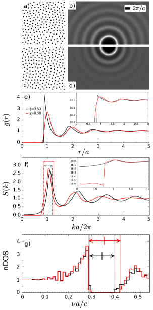
Photonic density of states—We study numerically the photonic properties of a dielectric system composed of silicon (dielectric constant or permittivity ) rods and walls derived from HD and SHU seed patterns. For the first protocol we place cylindrical rods (in three dimensions, disks in the plane) at the points of the seed pattern. We use a fixed rod radius , which leads to an area filling fraction of the two-dimensional plane with silicon, independent of and provided no two rods overlap. The no-overlap condition is almost exactly met in the relevant regime . We use the supercell method Joannopoulos et al. (2008) implemented in the open source code MIT Photonic Bands Johnson and Joannopoulos (2001) to obtain the normalized photonic density of states (nDOS). A finite sample (the supercell) is repeated periodically and the band structure calculated by following the path in reciprocal space. We accumulate a histogram of eigenfrequencies and compare it to the corresponding one for a homogeneous medium with a refractive index that best matches the first band (low energy) of both the structured and the homogeneous medium. In the next step, the effective refractive index of the structure and the width and position of the PBGs are obtained by direct analysis of the band structure 111Because we determine the PBG width directly from the band structure, the precision is higher than suggested from the bin width of the histogram, e.g. in Fig. 1(g).
The nDOS for the HD system with and for the SHU system with [Fig. 1(g)] are almost identical in TM polarization and resemble a typical nDOS of a photonic crystal. Apparently the structural similarity of the seed patterns translates into a corresponding similarity of the photonic band structure. In fact, the position and width of the PBG covers exactly the peak region of , Fig. 1(f), corresponding to Bragg scattering at the isotropic Brillouin zone.
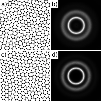
It is known Meade et al. (1993) that the placement of rods is a good ansatz to obtain a PBG in TM polarization but does not lead to the opening of a PBG in TE polarization, even for perfect crystals. Instead, in the second protocol, we perform the Delaunay triangulation of the seed pattern and connect the barycenters of neighboring triangles by walls (in three dimensions, bonds in the plane) to form a trivalent network 222In the process of triangulation and barycenter linking the number of network nodes (N) of the seed pattern doubles.. This protocol enforces a uniform structure with three bonds at each node, favouring the opening of a gap due to the local topology Florescu et al. (2009); Weaire (1971); Weaire and Thorpe (1971). We use a fixed wall thickness of . Finally, to enforce PBGs in both polarizations simultaneously, we combine the two protocols and form a decorated network consisting of rods (radius ) and Delaunay walls (thickness ) [Fig. 2]. All geometric parameters are optimized to yield a maximally wide PBG, see also supplemental material Sup . The results for the HD system and the SHU system in TM, TE polarization as well as in both polarizations simultaneously are equally similar Sup .
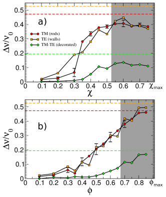
Next, we analyze the normalized PBG width for TM, TE and both polarizations simultaneously as a function of stealthiness and packing density . As shown in Fig. 3, the PBG is initially narrow but widens with increasing and . Interestingly, the central frequency of the PBG is almost unchanged at . also coincides with the PBG center of a hexagonal lattice with identical scatterer geometry and area filling fraction. For comparison we include in Fig. 3 results obtained when the seed pattern is the hexagonal lattice. In this case, the PBG is even wider, which suggests that the amorphous patterns attempt to asymptotically reach the crystal values but cannot exceed them – at least not for the two-dimensional structures considered here. The joint PBG for TM and TE polarization is generally narrower than the PBG for TM or TE polarization alone and typically reaches only a width of approximately for amorphous patterns and for the hexagonal lattice.
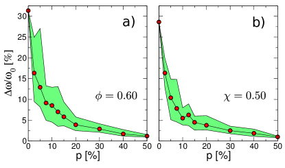
Robustness of the photonic band gap—Finally, we address briefly the influence of imperfections on the width of the PBG. Imperfections are unavoidable in the experimental realization of photonic materials and the robustness of the PBG is an important design parameter. For simplicity we restrict our analysis to the case of random link removal in the network of walls and for TE polarization, following the procedure described in Florescu et al. (2010). A percentage of links is removed randomly and for each value of we calculate the nDOS for ten different structures. As shown in Fig. 4, we find that the removal of links gradually reduces the width of the gap. Our results indicate that, within statistical error, the results are the same for the SHU and the HD structure. Moreover, our results are similar to those obtained for the corresponding hexagonal lattices of dielectric walls Florescu et al. (2010), see also supplemental material Sup .
Discussion and conclusion.—Our findings demonstrate that disordered packings in real and reciprocal space are equally suitable for generating isotropic PBG materials in two dimensions. SHU patterns restrict the accessible phase space in a different way, but are not found to be more efficient in opening wider PBGs than HD patterns. The parameters and acquire their meaning due to the presence of a maximum value, i.e. a value where the accessible phase space volume is zero, the system is fully constrained, and dynamics disappears. In the case of HDs this value is the packing density of the densest packing of disks in the hexagonal lattice, . For SHU patterns the maximum value is obtained once the excluded zone in reciprocal space touches the Bragg peaks. Interestingly, and for reasons that are unclear, our results suggest that SHU patterns converge towards the square lattice Sup after the appearance of intermediate stacked-slider phases with local hexagonal order Zhang et al. (2015), and thus . Since the phase space restrictions that are imposed by and are highly non-linear, no simple linear relationship exists between them well below their maximum value.
The characteristic length scale for the development of a PBG, the so-called Bragg length , is typically on the order of the characteristic structural length scale . Suppression of scattering at wave numbers smaller than , as targeted by hyperuniformity, should therefore play a marginal role in the formation of the PBG. Indeed, we believe that the emergence of a PBG is a side-effect of hyperuniformity. Increasing prevents scattering for and the intensity piles up, due to a sum rule, just above 333this point was first raised in discussions with Chris Henley, Cornell University, private communication (2014).. Suppression of scattering at small wave numbers and hyperuniformity (strictly or in approximation) are then natural consequences of the development of short-range order and vice versa.
In all cases studied the maximum bandwidth approaches the crystal values only asymptotically. The influence of defects is local and it affects the band gap most whenever such defects percolate as shown in Florescu et al. (2010). Moreover in Yang et al. (2010) it was found that the bandgap of polycrystalline photonic structures remains nearly unchanged from that of the perfect crystalline structure as long as the crystal domains are larger than a few times the Bragg length . These observations, taken together, suggest that the band gap formation is determined by local properties. Optimization of short-range order, in particular the tailoring of Bragg scattering at the isotropic Brillouin zone, and the appropriate topology are expected to be the key aspects for enforcing a photonic band gap in dielectric materials.
This research was supported by the National Science Foundation, Division of Materials Research Award No. DMR 1120923 (M.E., P.F.D., S.C.G.). S.C.G. acknowledges partial support by a Simons Investigator award from the Simons Foundation. This research was supported by the Swiss National Science Foundation through the National Centre of Competence in Research Bio-Inspired Materials and through project number 149867 (L.S.F.P, N.M., F.S.). N.M. acknowledges support by the Luxembourg National Research fund (project No. 3093332). L.S.F.P., N.M., and F.S. would like to thank Kevin Vynck for interesting discussions.
References
- Joannopoulos et al. (2008) J. D. Joannopoulos, S. G. Johnson, J. N. Winn, and R. D. Meade, Photonic Crystals: Molding the Flow of Light (Princeton University Press, 2008).
- López (2003) C. López, Advanced Materials 15, 1679 (2003).
- Parker et al. (2000) G. J. Parker, M. E. Zoorob, M. D. B. Charlton, J. J. Baumberg, and M. C. Netti, Nature 404, 740 (2000).
- Rechtsman et al. (2008) M. C. Rechtsman, H.-C. Jeong, P. M. Chaikin, S. Torquato, and P. J. Steinhardt, Physical Review Letters 101, 073902 (2008).
- Edagawa (2014) K. Edagawa, Science and Technology of Advanced Materials 15, 034805 (2014).
- Jin et al. (2001) C. Jin, X. Meng, B. Cheng, Z. Li, and D. Zhang, Physical Review B 63, 195107 (2001).
- Rockstuhl et al. (2006) C. Rockstuhl, U. Peschel, and F. Lederer, Optics Letters 31, 1741 (2006).
- Shi et al. (2013) L. Shi, Y. Zhang, B. Dong, T. Zhan, X. Liu, and J. Zi, Advanced Materials 25, 5314 (2013).
- Rojas-Ochoa et al. (2004) L. F. Rojas-Ochoa, J. M. Mendez-Alcaraz, J. J. Sáenz, P. Schurtenberger, and F. Scheffold, Physical Review Letters 93, 73903 (2004).
- Markoš and Soukoulis (2005) P. Markoš and C. M. Soukoulis, Physical Review B 71, 054201 (2005).
- Reufer et al. (2007) M. Reufer, L. F. Rojas-Ochoa, S. Eiden, J. J. S enz, and F. Scheffold, Applied Physics Letters 91, 171904 (2007).
- Galisteo-López et al. (2011) J. F. Galisteo-López, M. Ibisate, R. Sapienza, L. S. Froufe-Pérez, Á. Blanco, and C. López, Advanced Materials 23, 30 (2011).
- Rechtsman et al. (2011) M. Rechtsman, A. Szameit, F. Dreisow, M. Heinrich, R. Keil, S. Nolte, and M. Segev, Physical Review Letters 106, 193904 (2011).
- Izrailev et al. (2012) F. Izrailev, A. Krokhin, and N. Makarov, Physics Reports 512, 125 (2012).
- Wiersma (2013) D. S. Wiersma, Nature Photonics 7, 188 (2013).
- Conley et al. (2014) G. M. Conley, M. Burresi, F. Pratesi, K. Vynck, and D. S. Wiersma, Physical Review Letters 112, 143901 (2014).
- Haberko and Scheffold (2013) J. Haberko and F. Scheffold, Optics Express 21, 1057 (2013).
- Muller et al. (2014) N. Muller, J. Haberko, C. Marichy, and F. Scheffold, Advanced Optical Materials 2, 104 (2014).
- Sun et al. (2013) J. Sun, B. Bhushan, and J. Tong, RSC Advances 3, 14862 (2013).
- Lourtioz (2004) J.-M. Lourtioz, Nature Materials 3, 427 (2004).
- Man et al. (2013) W. Man, M. Florescu, E. P. Williamson, Y. He, S. R. Hashemizad, B. Y. C. Leung, D. R. Liner, S. Torquato, P. M. Chaikin, and P. J. Steinhardt, Proceedings of the National Academy of Sciences of the United States of America 110, 15886 (2013).
- Takeoka (2012) Y. Takeoka, Journal of Materials Chemistry 22, 23299 (2012).
- Park et al. (2014) J.-G. Park, S.-H. Kim, S. Magkiriadou, T. M. Choi, Y.-S. Kim, and V. N. Manoharan, Angewandte Chemie International Edition 53, 2899 (2014).
- Dyachenko et al. (2014) P. N. Dyachenko, J. J. do Rosário, E. W. Leib, A. Y. Petrov, R. Kubrin, G. A. Schneider, H. Weller, T. Vossmeyer, and M. Eich, ACS Photonics 1, 1127 (2014).
- Florescu et al. (2009) M. Florescu, S. Torquato, and P. J. Steinhardt, Proceedings of the National Academy of Sciences of the United States of America 106, 20658 (2009), arXiv:1007.3554 .
- Batten et al. (2008) R. D. Batten, F. H. Stillinger, and S. Torquato, Journal of Applied Physics 104, 033504 (2008).
- Leseur et al. (2015) O. Leseur, R. Pierrat, and R. Carminati, (2015), arXiv:1510.05807 .
- Edagawa et al. (2008) K. Edagawa, S. Kanoko, and M. Notomi, Physical Review Letters 100, 013901 (2008).
- Liew et al. (2011) S. F. Liew, J.-K. Yang, H. Noh, C. F. Schreck, E. R. Dufresne, C. S. O’Hern, and H. Cao, Physical Review A 84, 063818 (2011).
- Torquato et al. (2015) S. Torquato, G. Zhang, and F. Stillinger, Physical Review X 5, 021020 (2015).
- Donev et al. (2005) A. Donev, F. H. Stillinger, and S. Torquato, Physical Review Letters 95, 090604 (2005).
- Ikeda and Berthier (2015) A. Ikeda and L. Berthier, Physical Review E 92, 012309 (2015).
- (33) See Supplemental Material at http://link.aps.org/supplemental/XXX for additional text on methods, figures, and codes. .
- Bernard and Krauth (2011) E. P. Bernard and W. Krauth, Physical Review Letters 107, 155704 (2011).
- Engel et al. (2013) M. Engel, J. A. Anderson, S. C. Glotzer, M. Isobe, E. P. Bernard, and W. Krauth, Physical Review E 87, 042134 (2013).
- Johnson and Joannopoulos (2001) S. Johnson and J. Joannopoulos, Optics Express 8, 173 (2001).
- Note (1) Because we determine the PBG width directly from the band structure, the precision is higher than suggested from the bin width of the histogram, e.g. in Fig. 1(g).
- Meade et al. (1993) R. D. Meade, A. M. Rappe, K. D. Brommer, and J. D. Joannopoulos, Journal of the Optical Society of America B 10, 328 (1993).
- Note (2) In the process of triangulation and barycenter linking the number of network nodes (N) of the seed pattern doubles.
- Weaire (1971) D. Weaire, Physical Review Letters 26, 1541 (1971).
- Weaire and Thorpe (1971) D. Weaire and M. F. Thorpe, Physical Review B 4, 2508 (1971).
- Florescu et al. (2010) M. Florescu, S. Torquato, and P. J. Steinhardt, Applied Physics Letters 97, 201103 (2010).
- Zhang et al. (2015) G. Zhang, F. H. Stillinger, and S. Torquato, Physical Review E 92, 022119 (2015).
- Note (3) This point was first raised in discussions with Chris Henley, Cornell University, private communication (2014).
- Yang et al. (2010) J.-K. Yang, C. Schreck, H. Noh, S.-F. Liew, M. I. Guy, C. S. O’Hern, and H. Cao, Physical Review A 82, 053838 (2010).