Dipole Analysis of the Dielectric Function of Colour Dispersive Materials:
Application to Monoclinic Ga2O3
Abstract
We apply a generalized model for the determination and analysis of the dielectric function of optically anisotropic materials with colour dispersion to phonon modes and show that it can also be generalized to excitonic polarizabilities and electronic band-band transitions. We take into account that the tensor components of the dielectric function within the cartesian coordinate system are not independent from each other but are rather projections of the polarization of dipoles oscillating along directions defined by the, non-cartesian, crystal symmetry and polarizability. The dielectric function is then composed of a series of oscillators pointing in different directions. The application of this model is exemplarily demonstrated for monoclinic (-phase) Ga2O3 bulk single crystals. Using this model, we are able to relate electronic transitions observed in the dielectric function to atomic bond directions and orbitals in the real space crystal structure. For thin films revealing rotational domains we show that the optical biaxiality is reduced to uniaxial optical response.
I Introduction
For the understanding, design and fabrication of optoelectronic devices, the optical properties of the involved materials have to be known. A well established and powerful method for the determination of these properties is spectroscopic ellipsometry Azzam and Bashara (1977); Fujiwara (2007). We concentrate here on the dielectric function (DF), which is usually obtained by means of numerical model analysis of the experimental ellipsometry data and then often described by a series of line-shape model dielectric functions in order to deduce phonon properties, free charge carrier concentrations and the properties of electronic transitions (e.g Ref. Schubert, 2004; Fujiwara, 2007). For isotropic materials this method is well established. However, in recent years, optically anisotropic materials, as e.g. Ga2O3 Ueda et al. (1997); Yamaguchi (2004); Varley and Schleife (2015); Sturm et al. (2015), CdWO4 Jellison et al. (2011) and lutetium oxyorthosilicate Jellison et al. (2012), went into focus of research since they are promising candidates for optoelectronic applications in the UV spectral range. However, the determination of their optical and electronic properties is more challenging compared to isotropic materials since they depend on the crystal orientation. The dielectric function is represented by a (frequency-dependent) tensor and the determination of its components requires a series of measurements for various crystal orientations.
For (non-chiral) optically anisotropic materials, the dielectric function is in general a symmetric tensor consisting of six independent components Born and Wolf (1999), i.e.
| (1) |
Due to its symmetry, this tensor can be diagonalized independently for the real and imaginary part at each wavelength separately. In the transparent spectral range, i.e. for vanishing imaginary part, the diagonal elements are the semi-principal axes of the ellipsoid of wave normals and are often called dielectric axes. For materials with monoclinic or triclinic crystal structure, the orientation of the dielectric axes depends on the wavelength and is often called colour dispersion. In the spectral rang with non-vanishing absorption, the situation becomes even more complex. Due to the independent diagonalizability of the tensor (1) for the real and imaginary part, the corresponding dielectric axes in general do not coincide which each other. Thus, in general, four dielectric axes are present. For these classes of materials only few reports on the determination of the full dielectric tensor exists, e.g. for -PTCDA Alonso et al. (2002), pentacene Dressel et al. (2008), BiFeO3 Schmidt et al. (2015), CdWO4 Jellison et al. (2011), K2Cr2O7 Höfer et al. (2014), CuSOH2O Höfer et al. (2013) and effective anisotropic materials as e.g. slanted columnar films Schmidt and Schubert (2013). Most of these works are limited to the determination of the line shape of the dielectric function, treating each tensor component of the DF independently of each other. This can, from a technical point of view, result in large correlations between the individual tensor elements causing non-physical results. More importantly, the deeper nature of polarizabilities in the material, like phonons, excitons, and electronic band-band transitions, cannot be explored this way. Thus, lineshape model dielectic functions (MDF) representing the oscillators properties like energy, amplitude, broadening, and even oscillation direction in a meaningful and physical correct way have to be used.
Facing this, Dressel et al. Dressel et al. (2008) proposed an approach assuming that the dipole moments are aligned to three polarization axis which should coincide with the crystallographic axes. Taking this model into account, the dielectric tensor is fully described by its three independent principal elements and the known angles between the crystallographic axis. However, as a consequence of this approach the principal axes of the indicatrix (related to the real part of ) coincide with those of the conductivity tensor (related to the imaginary part of ) which is not generally valid as shown for instance for CdWO4 Jellison et al. (2011) and Ga2O3 Sturm et al. (2015). To overcome this problem, Höfer et al. Höfer et al. (2013, 2014) used for the infrared spectral range a model, developed earlier by Emslie et al. Emslie and Aronson (1983), which consists of a sum of damped Lorentz oscillators individually aligned to the axes of their respective dipole moments. For phonons, these axes are related to the atomic elongations and thus to some extent to the crystallographic axes. Further, their dissipative spectral range is usually narrow. Thus the question arises if such a model also can be applied to spectrally widespread excitations like electronic band-band transitions, which consist of numbers of individual dipoles whose axes are connected to overlapping atomic orbitals of various symmetry and therefore not necessarily coincide with crystallographic directions. Further the density of states (DOS) of the electronic band structure is distributed within a wide energy range in a complex manner causing non-symmetric line-shapes of the imaginary part of the dielectric function which spectrally overlap for different contributions and directions.
Here we demonstrate that the sketched approach is generally valid for all kinds of excitations. We demonstrate this exemplarily for monoclinic Ga2O3 (-phase) single crystals and thin films in the spectral range from infrared to vacuum ultraviolet. We show that this model provides a deep insight in electronic properties of the materials: Comparing the directions of the electronic polarizabilities obtained by modeling the experimental ellipsometry data using lineshape MDF to the real space atomic arrangement in the crystal and considering theoretical calculated electron density distribution as well as orbital-resolved DOS, allows us to assign the observed transitions to individual orbitals.
The paper is organized as follows: In Sec. II, we discuss at first the dielectric tensor for all crystal symmetries and its composition. After that we demonstrate its applicability to the case of -Ga2O3 single crystals in the infrared and ultraviolet spectral range. Finally, we show by means of a practically relevant -Ga2O3 thin film which exhibit rotation domains that the approach of using directed transitions explains the effective uniaxial properties of the film and enhances the sensitivity to the out-of plane component of the dielectric tensor.
II Dielectric function
The optical response of a material is determined in first order by dipole excitations, e.g. optical phonons, electronic band-band transitions or excitons which in sum are represented by the dielectric function. For isotropic materials, the corresponding dipole moment or polarization direction of each excitation is macroscopically equally distributed in all spatial directions, resulting in an isotropic dielectric function, i.e. it is a scalar written as
| (2) |
with being the number of excitations/oscillators. The situation changes for materials with crystal structure symmetry lower than the cubic one. In this case the excitations generally differ between the crystallographic directions in energy, amplitude, broadening, and even in the spatial direction of their dipole moment, and thus the DF is a tensor (Eq. (1)).
Let being the dielectric response of the excitation and the coordinate system is chosen (without loosing generality) in such way that the polarization direction is along the -axis. The only non-zero component is then given by , i.e. . However, the polarization direction of the excitation and the experimental coordinate system do not coincide with each other in general and a coordinate transformation has to be performed, independently for each transition. The entire dielectric tensor then can be expressed by
| (3) |
with and being Euler angles, which are in general different for each excitation, and being the rotation matrix. The advantage of this expression is that the components of the resultant dielectric tensor in the Cartesian coordinate system are not independent of each other but rather composed of the respective projected part of the excitation’s line-shape function according to the directions of their individual dipole moment. For the entire dielectric function it follows that, due to the finite broadening of each excitation and by considering Kramers-Kronig relation, the orientation of the principal tensor axes of the real and imaginary parts differ from each other as it is well known and observed in experiments e.g. for CdWO4 Jellison et al. (2011) and Ga2O3 Sturm et al. (2015).
Equation (3) represents the general case which has to be used for triclinic crystals and can be simplified depending on the crystal symmetry. Crystals with monoclinic structure exhibit one symmetry axes, representing a rotation axis or the normal of a mirror plane (or both), which we identify in the following with the -direction. The plane perpendicular to , the --plane, reveals no symmetry which defines a Cartesian coordinate system preferentially. Therefore, from symmetry arguments, considering dipoles polarized either along or in the --plane, one can simplify Eq. (3) to
| (4) |
with and being the contribution of the respective directions. and represent the number of excitations with the corresponding polarization directions and as we define the angle between the polarization direction and the -axes within the --plane. This leads to the well known form of the dielectric tensor given by
| (5) |
A further simplification can be made for orthorhombic materials containing three orthogonal twofold rotation symmetry axis, leading to
| (6) |
a dielectric function tensor which contains only diagonal elements. In the case of uniaxial materials, e.g. those with a hexagonal symmetry, and holds. For isotropic material, the numbers of oscillators in all three directions is the same and therefore the dielectric tensor reduces to the scalar given by Eq. (2).
For practical application Eq. (3) has to be further modified. The real and imaginary parts of the dielectric function are connected with each other by the Kramers-Kronig relation. Contributions of excitations at energies higher than the investigated spectral range to the real part of the DF have to be considered. These contributions are usually described by a pole function. In the case presented here, this means that the identity in Eq. (3) has to be replaced by a real valued tensor with the form given by the corresponding crystal structure where each component is represented by a pole function.
III Experimental
By using the approach presented in Sec. II and line-shape MDFs, the parametrised dielectric function of -Ga2O3 bulk single crystals and thin films was determined in the mid-infrared up to the vacuum-ultraviolet spectral range by means of generalized spectroscopic ellipsometry.
Ga2O3 crystallizes at ambient conditions in monoclinic crystal structure, the so-called -phase (Fig. 4). The angle between the non-orthogonal - and -axis is Geller (1960) resulting in a non-vanishing off-diagonal element of the dielectric tensor within the Cartesian coordinate system Sturm et al. (2015); Schubert et al. (2016). We investigated two single side polished bulk single crystals from Tamura Corporation with and orientation, allowing access to all components of the dielectric tensor. X-ray diffraction (XRD) measurements does not reveal any hints for the presence of rotation domains, twins or in-plane domains. More details can be found in Ref. Sturm et al., 2015. The thin film was deposited on a -plane oriented sapphire substrate by means of pulsed laser deposition (PLD) at . After deposition, the sample was annealed for at and a oxygen partial pressure of . XRD measurements confirm the monoclinic crystal structure of the film and the surface orientation was determined to be . In contrast to the bulk single crystals, six rotation domains are observed which are rotated against each other by an angle of . Splith et al. (2014) In contrast to bulk single crystals which reveal a smooth surface without atomic steps, the surface roughness of the thin film was determined to be
In spectroscopic ellipsometry, the change of the polarization state of light after interaction with a sample is determined. In the general case, this is expressed by means of the Mueller matrix (MM, ) which connects the Stokes vectors of the incident (reflected) light () by . In the special case where no energy transfer between orthogonal polarization eigenmodes of the probe light takes place, like for isotropic samples or optically uniaxial samples with the optical axis pointing along the surface normal (as the case for the thin film, cf. Sec. V), the change of the polarization state is expressed by the ratio of the complex reflection coefficients, i.e. . The index represents the polarization of the light polarized parallel () or perpendicular (), respectively, to the plane of incidence which is spanned by the surface normal and the light beams propagation direction.
For the determination of the DF, the experimental data are analyzed by transfer-matrix calculations considering a layer stack model. For the bulk single crystals, the model consists of a semi-infinite substrate (Ga2O3 itself) and a surface layer accounting for some roughness or contaminations. For the infrared spectral range the surface layer can be neglected. For the thin film the model consists of a -oriented sapphire substrate, the Ga2O3 thin film layer and the surface layer. The dielectric function of sapphire was taken from the literature Yao and Yan (1999). The surface layer was modelled using an effective medium approximation (EMA) Bruggeman (1935) mixing the DF of Ga2O3 and void by for the bulk single crystals.Sturm et al. (2015) For the thin film this fraction was chosen as parameter and the best match between experiment and calculated spectra was obtained for . In the following we choose our coordinate system in such way, that -axis, -axis and .
IV Bulk Single Crystals
IV.1 Infrared spectral range
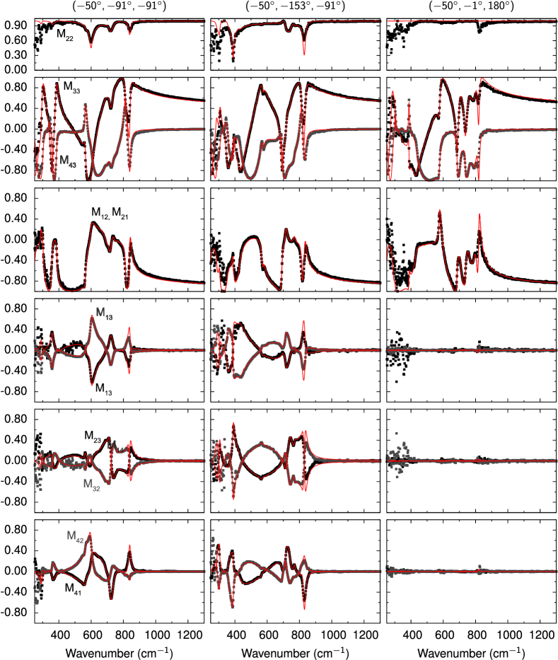
The MM in the infrared spectral ( ()) range was measured at angles of incidence of , and for different in-plane rotations, i.e. rotating the crystal around its surface normal by , and . For selected orientations the recorded spectra are shown in Fig. 1. The non-vanishing block-off-diagonal elements of the MM demonstrate the optically anisotropic character of the sample.
The dielectric function in the infrared spectral range is determined by phonon and free charge carrier oscillations. The bulk single crystals are not intentionally doped, the latter contribution can be neglected for the spectral range investigated here. Therefore, only phonons have to be considered and their contribution is described by Lorentzian oscillators: Yu and Cardona (2010)
| (7) |
with , and being the amplitude, energy and broadening of the phonon mode, respectively. The calculated MM spectra are shown in Fig. 1 as red solid lines yielding good agreement with the experimental ones. Note, that a similarly good match is obtained by using a Kramers-Kronig consistent numerical analysis and consider the four components of the DF (Eq. (5)) to be independent from each other.
In the investigated spectral range, 9 of the totally 12 optical infrared active phonon modes are observable. Their properties are summarized in Tab. 1. For the modes which have a dipole moment in the - plane (-symmetry) the polarization direction with respect to the -axis is given by the angle , which was found to differ for each phonon mode. This is also in agreement with the results recently reported by Schubert et al.Schubert et al. (2016) The phonon mode was not observable in our experiment. This can be attributed to the weak sensitivity to this mode caused by its low amplitude which is predicted by ab-initio calculations (see below) and to the pronounced noise caused by the low sensitivity of the detector of our setup in this spectral range. Further, for the mode only the frequency is given since also the large noise in this spectral range and the probable spectral overlap with prohibit the determination of its dipole direction.
| - | - | 0.01 | - | - | - | - | 160.7 | 155 | 154.8 | 155 | 155.7 | 141.6 | |
| - | - | 0.41 | - | - | 101 | - | 224.3 | 250 | 213.7 | 216 | 202.4 | 187.5 | |
| 92 | - | 0.33 | 8 | - | 176 | 253 | 267.3 | 290 | 262.3 | 300 | 260.4 | 251.6 | |
| - | - | 0.03 | - | - | 39 | - | 281.9 | 310 | 279.1 | 337 | 289.7 | 265.3 | |
| 51 | - | 0.50 | 21 | - | - | 295 | 300.5 | n.o. | 296.6 | 352 | 327.5 | 296.2 | |
| 86 | 0.20 | 0.16 | 4 | 166 | 173 | 357 | 361.0 | 375 | 356.8 | 374 | 365.8 | 343.6 | |
| 82 | 0.96 | 0.96 | 17 | 46 | 47 | 430 | 434.2 | 455 | 432.5 | 500 | 446.8 | 410.5 | |
| 83 | 0.77 | 0.78 | 13 | - | 447 | 447.0 | 525 | 448.6 | 526 | 475.7 | 383.5 | ||
| 73 | 1.00 | 1.00 | 15 | 128 | 130 | 572 | 560.8 | 640 | 572.5 | 626 | 589.9 | 574.3 | |
| 73 | 0.39 | 0.43 | 5 | - | 662 | 665.8 | 668 | 663.2 | 656 | 678.4 | 647.9 | ||
| 32 | 0.25 | 0.23 | 7 | 28 | 0 | 691 | 692.5 | 692 | 692.4 | 720 | 705.8 | 672.6 | |
| 10 | 0.13 | 0.13 | 11 | 74 | 76 | 743 | 742.5 | 731 | 743.5 | 760 | 753.8 | 741.6 | |
| this work | Ref. Dohy et al.,1982 | Ref. Schubert et al.,2016 | Ref. Dohy et al.,1982 | Ref. Schubert et al.,2016 | Ref. Liu et al.,2007 | ||||||||
For comparison we calculated the phonon modes by ab-initio calculations based on the B3LYP hybrid functional approach implemented in the CRYSTAL14 code Kranert et al. (2016). Thereby we used the basis set of Pandey et al. Pandey et al. (1994) for gallium and of Valenzano et al. Valenzano et al. (2006) for oxygen, which we slightly modified, and 150 -points in the irreducible Brillouin zone. The truncation criteria defined by CRYSTAL14 code given by five tolerance set to 8,8,8,8, and 16 for our calculations were used for the Coulomb and exchange infinite sums. Further we used a tolerance of the energy convergence of Hartree. All input parameters and calculation conditions can be found in Ref. Kranert et al., 2016. The calculated lattice parameters are , and , in reasonable agreement with those reported in the literature Geller (1960). The corresponding phonon mode energies, oscillator strength and the direction of the dipoles are also given in Tab. 1 and are in excellent agreement with those determined by ellipsometry. The excellent agreement is not restricted to the infrared active phonon modes but is also obtained for the Raman active modes Kranert et al. (2016).
IV.2 Ultraviolet spectral range
The numeric DF in the UV spectral range was recently reported by us, obtained by using a Kramers-Kronig consistent numerical analysis Sturm et al. (2015). In order to extract the properties of the contributing electronic transitions, e.g. energy and electronic orbitals involved, and to demonstrate the universal applicability of Eq. (3) for electronic transitions we analysed the contribution of each transition to the entire DF by using line-shape model dielectric functions. Symmetry consideration and band structure propertiesSturm et al. (2015) yield that the transitions are polarized either along the -axes or within the --plane. Thus the DF can be written as in Eq. (4) with a set of excitonic transitions and Gaußian oscillators. We have been shown by density functional theory calculations combined with many-body perturbation theory including quasiparticle and excitonic effects Sturm et al. (2015), that the DF in the spectral range from the fundamental absorption edge on up to some eV higher are dominated by excitonic correlation effects. Thus, several excitonic contributions have been considered in modeling and were described by a model dielectric function developed by C. Tanguy for Wannier excitons taking into account bound and unbound states. Tanguy (1995, 1996, 1999) The contribution of weakly pronounced band-band-transitions where summarized by using a Gaussian oscillator. A further Gaussian oscillator was included to consider contributions of transitions at energies higher than the investigated spectral range due to their spectral broadening. These contributions together with the pole function were considered for each dielectric tensor component independently because they may originate from different transitions.
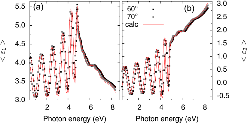
The experimentally recorded and the calculated spectra of the MM elements are shown for selected orientations in Fig. 2, yielding good agreement. The difference between the experimental and the calculated spectra for energies was also observed by using the above mentioned numerical Kramers-Kronig consistent analysis and might be caused by the limitation of the used approach for the description of the surface layer.Sturm et al. (2015) This can be attributed to the fact that the sensitivity to this layer is strongly enhanced in this spectral range due to the enhanced absorption and therefore reduced penetration depth.
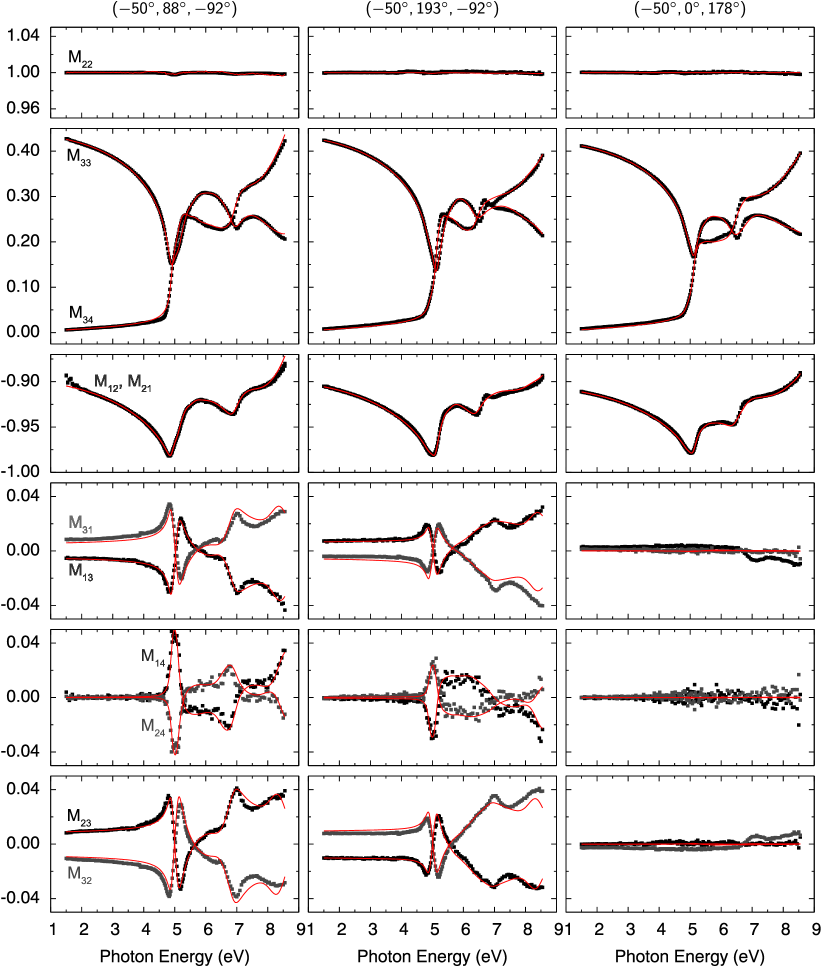
The parameters of the best-match MDF are summarized in Tab. 2 and 3. We extracted a exciton binding energy of about for all contributions. Note that we considered the same exciton binding energy for all excitonic transitions because of the strong correlation between energy of the fundamental bound state and the corresponding binding energy.
| label | direction | Type | ||||
| (eV) | (meV) | (∘) | ||||
| - | Exciton | 15.0 | 4.88 | 70 | 110 | |
| - | Exciton | 18.0 | 5.10 | 800 | 17 | |
| - | Exciton | 14.9 | 6.41 | 210 | 41 | |
| - | Exciton | 28.0 | 6.89 | 190 | 121 | |
| - | Gauss | 0.27 | 6.14 | 1,343 | 124 | |
| Exciton | 8.3 | 5.41 | 75 | |||
| Exciton | 20.1 | 5.75 | 139 | |||
| Exciton | 7.0 | 6.93 | 253 |
| Gauss | Pole | |||||
| A | ||||||
| (eV) | (eV) | (eV) | A | |||
| 2.64 | 9.69 | 2.7 | 200.8 | 15.5 | 0.907 | |
| 1.81 | 9.78 | 3.8 | 52.7 | 10.5 | 1.392 | |
| 1.84 | 8.99 | 1.7 | 91.5 | 11.9 | 1.126 | |
| 0.26 | 8.49 | 0.5 | -0.086 | |||
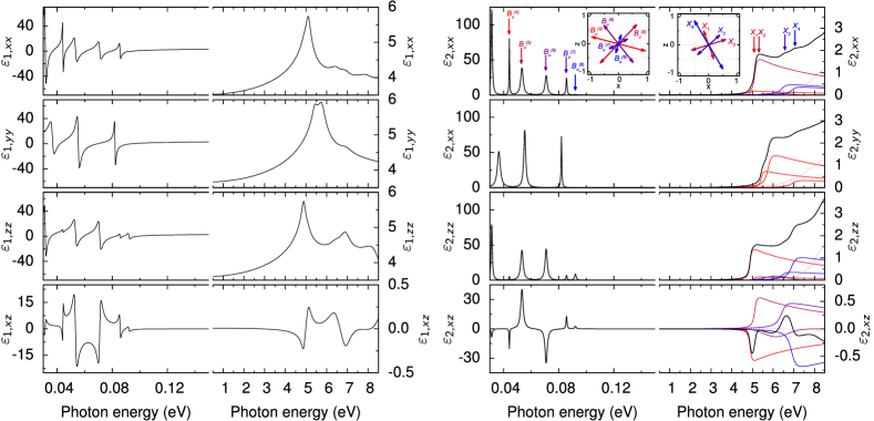
The dispersion of the tensor elements for the entire investigated spectral range is shown in Fig. 3. The contributions of excitonic transitions to are shown as red solid lines. The orientation of the corresponding dipole moments in the --plane is indicated by the arrows in the inset. In agreement with our theoretical calculations and the numeric MDF,Sturm et al. (2015) the two energetically lowest transitions (labeled as and ) are strongly polarized along the - and -direction, respectively. At higher energies, there are transitions along -axis (-axis) and within the --plane (--plane).
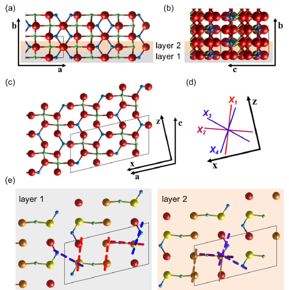
Based on calculated charge distribution Litimein et al. (2009) and atomic arrangement within the --plane (--plane), we relate the directions of the dipole moments of all four pronounced excitonic excitations within this plane ( …), as obtained from the ellipsometry model, to atomic bonds in the crystal structure as shown in Fig. 4. For transitions along , no direct assignment to individual orbitals was possible because of the complex distribution of atomic bonds. Please note that the uncertainty in the experimentally determined dipole moment directions amounts to up to 10∘, caused by the simplification due to the used model functions, which summarize spectrally over different individual transitions. As all these transitions reveal no contribution to the dielectric tensor component , only bonds located solely within the sub-planes of the --plane (--plane) are considered (cf. Fig 4). It is found that all excitonic transitions but the first one, which appears to take place between oxygen atoms, are between differently coordinated gallium and oxygen. In the following discussion we will use the nomenclature given by Geller Geller (1960) and label the tetrahedrally and octahedrally coordinated Ga atoms as Ga(I) and Ga(II), respectively, while the three different sites of the oxygen atoms are labeled as O(I), O(II) and (OIII) (cf. Fig. 4).
Band structure calculations reveal that the uppermost valence bands are dominated by oxygen -orbitals, while the DOS of the lowest conduction bands is composed of almost equal contributions from Ga-, O-, and O- orbitals.Yamaguchi (2004); Litimein et al. (2009); He et al. (2006) Thus, dipole allowed transitions can take place from O- orbitals to Ga- and O- orbitals. It turns out that the states near the conduction band minimum are preferentially determined by octahedrally coordinated Ga(II). Litimein et al. (2009) This is reflected by the assignment of the dipole directions to the atomic bonds in Fig. 4. It turns out that the transition , almost directed along () involves O and Ga(II) and also reveals a high amplitude in the DF. Ga(II) is located between O(II) and O(III). But the dipole direction only fits to the bond Ga(II)-O(III), so it seems that transitions to Ga(II) states in the conduction band only appear when O(III) is involved and are not possible involving O(II). This can be understood considering the coordination of the O-atoms, which is higher (6 bonds) for O(II), suggesting the orbitals to be more -like compared to O(III) (4 bonds) which dominate the DOS near the valence band maximum. The transitions and are assigned to take place between Ga(I) and O(III). The directions obtained from model analysis of the DF does not fit as good as for transition , maybe caused in correlation effects due to spectral overlap of different contributions to the DF. Finally, transition , directed almost along , was assigned to take place either between O(I) and O(III) or between two O(II) atoms, or both. While the first possibility involves differently coordinated atoms suggesting dipole allowed transitions between - and -like orbitals, the second possibility involves only highly coordinated atoms (-like character) and thus should be dipole forbidden. The relatively high amplitude of this transition is not clear at first place, because following Ref. Litimein et al., 2009, the charge density between the involved atoms and also the DOS of the oxygen orbitals in the conduction band is predicted to be relatively weak.
These results nicely demonstrate the potential of the used model approach for the dielectric tensor to gain deep insight into electronic properties of highly anisotropic materials.
V thin film
As mentioned above, the PLD grown -Ga2O3 thin film exhibit surface orientation with 6 in-plane rotation domains, rotated by multiples of . As their size is much smaller than the optically probed sample area of about mm2, the measured optical response is determined by an average over these domains. For uniform distribution of these rotation domains, the effective dielectric function is given by
| (8) |
with the rotation angle of the rotation domain ( and being the rotation matrix around the surface normal. Equation (8) is similar to those of a uniaxial material with and ( and : perpendicular and parallel to the optical axis) with orientation of the effective optical axis along the surface normal. Note that and are the tensor components for the coordinate system with the - and axis parallel and perpendicular to the sample surface, respectively.
For such samples with the sensitivity to is usually limited due to the high index of refraction of the investigated material resulting in a propagation direction of the wave within the sample with only very small angles off the optical axis. But there is a finite projection of the electro-magnetic field strength onto the optical axis and thus the optical response is determined by and in any case, which have to be considered in order to obtain a physical meaningful dielectric function Shokhovets et al. (2010). However, in contrast to a homogeneous uniaxial material, those effective and are not independent from each other. As shown in Sec. II and demonstrated in Sec. IV the components and reflect the same transitions and are determined by the projection of their amplitudes ( is the angle of the oscillation direction of the individual dipoles with respect to the sample surface). This offers in the present case more sensitivity for determination of the tensor component as compared to homogeneous uniaxial materials.
The uniaxial behaviour of the film with the optical axis parallel to the surface normal is reflected by vanishing off-diagonal elements of the MM. Therefore, standard ellipsometry is sufficient for measuring the full optical response (cf. Sec. III). The experimental data are shown in Fig. 5 in terms of the pseudo dielectric functionFujiwara (2007)
| (9) |
with angle of incidence . Below oscillations due to multiple reflection interferences caused by the interfaces within the sample are observed which vanish with the onset of the absorption at higher energies.
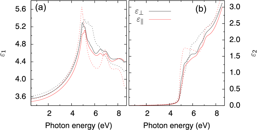
For the parametric model of the dielectric function of the thin film we used the same set of model dielectric functions as for the bulk single crystal. The calculated spectra are shown as red solid lines in Fig. 5 and a good agreement between the experimental and calculated data is apparent. The tensor components of the dielectric function of the thin film are shown in Fig. 6. For comparison, the components calculated from DF of the bulk single crystal by using Eq. (8) are shown as dashed lines. For the thin film, we needed to adjust energies and amplitudes of the transitions and even the dipoles’ orientation angles within the --plane (--plane). Compared to the DF of the single crystal a blue-shift of the transition energies up to and a lowering of the oscillator strengths is observed for the thin film. The reduced oscillator strength in the investigated spectral range cannot explain the lowering of the real part of the dielectric constant and therewith of the index of refraction in the visible spectral range alone. Therefore, the reduced refractive index indicates also a reduced oscillator strength of the high energy transitions compared to the bulk single crystal. We relate these changes of the DF properties compared to the bulk single crystal on the one hand to crystal imperfections typically lowering the oscillator strength of electronic transitions by dissipative processes. On the other hand also strain will be possibly present in the thin film, causing changes in the bond length and maybe also torsion of the unit cell causing different dipole moment orientations.
VI Summary
We have determined the dielectric function of -Ga2O3 by using a generalized oscillator model taking into account the direction of the dipole moments for each transition. Within this model, the components of the dielectric tensor within the cartesian coordinate system are not independent from each other but are determined by the projection of the corresponding dipole direction. In doing so, we could determine the tensor components of the DF of -Ga2O3 bulk single crystals and thin films. By means of the determined direction of the dipoles we assign the involved orbitals for the observed transitions. For the thin film we showed that the presence of rotation domains leads to the formation of an effective uniaxial material. The sensitivity to the out-of-plane component of the dielectric tensor is enhanced compared to pure uniaxial materials since it is connected to the in-plane component. This allows a precise determination of this component even if the optical axis is perpendicular to the surface, which is relevant for applications in optoelectronics.
Acknowledgements.
We thank Hannes Krauß, Vitaly Zviagin and Steffen Richter for the support of the ellipsometry measurements. This work was supported by the Deutsche Forschungsgemeinschaft within Sonderforschungsbereich 762 - ”Functionality of Oxide Interfaces”. We also acknowledge financial support of the Austrian Fond zur Förderung der Wissenschaftlichen Forschung in the framework of SFB25 - ”Infrared Optical Nanostructures”.References
- Azzam and Bashara (1977) R. Azzam and N. Bashara, Ellipsometry and Polarized Light (North-Holland, 1977).
- Fujiwara (2007) H. Fujiwara, Spectroscopic Ellipsometry: Principles and Applications, 1st ed. (John Wiley & Sons, 2007).
- Schubert (2004) M. Schubert, Infrared Ellipsometry on Semiconductor Layer Structures: Phonons, Plasmons, and Polaritons (Springer Tracts in Modern Physics) (Springer-Verlag Berlin Heidelberg, 2004).
- Ueda et al. (1997) N. Ueda, H. Hosono, R. Waseda, and H. Kawazoe, Appl. Phys. Lett. 71, 933 (1997).
- Yamaguchi (2004) K. Yamaguchi, Solid State Commun. 131, 739 (2004).
- Varley and Schleife (2015) J. B. Varley and A. Schleife, Semicond. Sci. Technol. 30, 24010 (2015).
- Sturm et al. (2015) C. Sturm, J. Furthmüller, F. Bechstedt, R. Schmidt-Grund, and M. Grundmann, APL Mater. 3, 106106 (2015).
- Jellison et al. (2011) G. E. Jellison, M. A. McGuire, L. A. Boatner, J. D. Budai, E. D. Specht, and D. J. Singh, Phys. Rev. B 84, 195439 (2011).
- Jellison et al. (2012) G. E. Jellison, E. D. Specht, L. A. Boatner, D. J. Singh, and C. L. Melcher, Journal of Applied Physics 112, 063524 (2012), http://dx.doi.org/10.1063/1.4752421.
- Born and Wolf (1999) M. Born and E. Wolf, Principles of Optics: Electromagnetic Theory of Propagation, Interference and Diffraction of Light, 7th ed. (Cambridge University Press, 1999).
- Alonso et al. (2002) M. Alonso, M. Garriga, N. Karl, J. Ossó, and F. Schreiber, Organic Electronics 3, 23 (2002).
- Dressel et al. (2008) M. Dressel, B. Gompf, D. Faltermeier, A. K. Tripathi, J. Pflaum, and M. Schubert, Opt. Express 16, 19770 (2008).
- Schmidt et al. (2015) D. Schmidt, L. You, X. Chi, J. Wang, and A. Rusydi, Phys. Rev. B 92, 075310 (2015).
- Höfer et al. (2014) S. Höfer, J. Popp, and T. G. Mayerhöfer, Vibrational Spectroscopy 72, 111 (2014).
- Höfer et al. (2013) S. Höfer, J. Popp, and T. G. Mayerhöfer, Vibrational Spectroscopy 67, 44 (2013).
- Schmidt and Schubert (2013) D. Schmidt and M. Schubert, J. Appl. Phys. 114, 083510 (2013).
- Emslie and Aronson (1983) A. G. Emslie and J. R. Aronson, J. Opt. Soc. Am. 73, 916 (1983).
- Geller (1960) S. Geller, J. Chem. Phys. 33, 676 (1960).
- Schubert et al. (2016) M. Schubert, R. Korlacki, S. Knight, T. Hofmann, S. Schöche, V. Darakchieva, E. Janzén, B. Monemar, D. Gogova, Q.-T. Thieu, R. Togashi, H. Murakami, Y. Kumagai, K. Goto, A. Kuramata, S. Yamakoshi, and M. Higashiwaki, arXiv:1512.08590 (2016).
- Splith et al. (2014) D. Splith, S. Müller, F. Schmidt, H. von Wenckstern, J. J. van Rensburg, W. E. Meyer, and M. Grundmann, physica status solidi (a) 211, 40 (2014).
- Yao and Yan (1999) D. P. H. Yao and C. H. Yan, J. Appl. Phys. 85, 6716 (1999).
- Bruggeman (1935) D. A. G. Bruggeman, Ann. Physik 24, 636 (1935).
- Yu and Cardona (2010) P. Yu and M. Cardona, Fundamentals of Semiconductors: Physics and Materials Properties (Graduate Texts in Physics), 4th ed. (Springer, 2010).
- Dohy et al. (1982) D. Dohy, G. Lucazeau, and A. Revcolevschi, Journal of Solid State Chemistry 45, 180 (1982).
- Liu et al. (2007) B. Liu, M. Gu, and X. Liu, Appl. Phys. Lett. 91, 172102 (2007), http://dx.doi.org/10.1063/1.2800792.
- Kranert et al. (2016) C. Kranert, C. Sturm, R. Schmidt-Grund, and M. Grundmann, submitted (2016).
- Pandey et al. (1994) R. Pandey, J. E. Jaffe, and N. M. Harrison, Journal of Physics and Chemistry of Solids 55, 1357 (1994).
- Valenzano et al. (2006) L. Valenzano, F. J. Torres, K. Doll, F. Pascale, C. M. Zicovich-Wilson, and R. Dovesi, Z. Phys. Chem. 220, 893 (2006).
- Tanguy (1995) C. Tanguy, Phys. Rev. Lett. 75, 4090 (1995).
- Tanguy (1996) C. Tanguy, Phys. Rev. Lett. 76, 716 (1996).
- Tanguy (1999) C. Tanguy, Phys. Rev. B 60, 10660 (1999).
- Momma and Izumi (2011) K. Momma and F. Izumi, J. Appl. Crystallogr. 44, 1272 (2011).
- Litimein et al. (2009) F. Litimein, D. Rached, R. Khenata, and H. Baltache, J. Alloys Compd. 488, 148 (2009).
- He et al. (2006) H. He, M. a. Blanco, and R. Pandey, Appl. Phys. Lett. 88, 261904 (2006).
- Shokhovets et al. (2010) S. Shokhovets, L. Spieß, and G. Gobsch, Journal of Applied Physics 107, 023509 (2010), http://dx.doi.org/10.1063/1.3285485.