Interfacial Spin-Orbit Torque without Bulk Spin-Orbit Coupling
Abstract
An electric current in the presence of spin-orbit coupling can generate a spin accumulation that exerts torques on a nearby magnetization. We demonstrate that, even in the absence of materials with strong bulk spin-orbit coupling, a torque can arise solely due to interfacial spin-orbit coupling, namely Rashba-Eldestein effects at metal/insulator interfaces. In magnetically soft NiFe sandwiched between a weak spin-orbit metal (Ti) and insulator (Al2O3), this torque appears as an effective field, which is significantly larger than the Oersted field and sensitive to insertion of an additional layer between NiFe and Al2O3. Our findings point to new routes for tuning spin-orbit torques by engineering interfacial electric dipoles.
An electric current in a thin film with spin-orbit coupling can produce a spin accumulation Edelstein1990 ; Hoffmann2013 ; Sinova2015 , which can then exert sizable torques on magnetic moments Manchon2008 ; Gambardella2011a ; Haney2013a ; Brataas2014 . First demonstrated in a ferromagnetic semiconductor Chernyshov2009 , “spin-orbit torques” are nowadays studied in room-temperature ferromagnetic metals (FMs) interfaced with heavy metals (HMs) with strong spin-orbit coupling, such as Pt, Ta, and W Liu2012d ; Fan2013 ; Fan2014 ; Pai2014 ; Miron2011 ; Skinner2014 ; Kawaguchi2015 ; Allen2015 ; Garello2013 ; Kim2013a ; Avci2014 ; Liu2014b ; Emori2014c ; Qiu2015 ; Akyol2015 ; Sato2016 . These torques can arise from (1) spin-dependent scattering of conduction electrons in the bulk of the HM, i.e., the spin-Hall effect Hoffmann2013 ; Sinova2015 ; Liu2012d ; Fan2013 ; Fan2014 ; Pai2014 , and (2) momentum-dependent spin polarization at the HM/FM interface, i.e., the Rashba-Edelstein effect Edelstein1990 ; Gambardella2011a ; Miron2011 ; Skinner2014 ; Kawaguchi2015 ; Allen2015 . Since a HM/FM system can exhibit either or both of these spin-orbit effects, it can be a challenge to distinguish the spin-Hall and Rashba-Edelstein contributions Garello2013 ; Kim2013a ; Haney2013a ; Brataas2014 ; Sinova2015 . Spin-orbit torques may be further influenced by spin scattering Chen2015b or proximity-induced magnetization Zhang2015c at the HM/FM interface. Moreover, in many cases Miron2011 ; Liu2012d ; Skinner2014 ; Kawaguchi2015 ; Allen2015 ; Fan2013 ; Fan2014 ; Pai2014 ; Avci2014 ; Garello2013 ; Kim2013a ; Liu2014b ; Emori2014c ; Qiu2015 ; Akyol2015 ; Sato2016 , the FM interfaced on one side with a HM is interfaced on the other with an insulating material, and the electric dipole at the FM/insulator interface Xu2012 ; Ibrahim2016 may also give rise to a Rashba-Edelstein effect. Recent studies Liu2014b ; Emori2014c ; Qiu2015 ; Akyol2015 ; Sato2016 indeed suggest nontrivial influences from insulating-oxide capping layers in perpendicularly-magnetized HM/FM systems. However, with the FM only 1 nm thick Liu2014b ; Emori2014c ; Qiu2015 ; Akyol2015 ; Sato2016 , changing the composition of the capping layer may modify the ultrathin FM and hence the HM/FM interface. The points above make it difficult to disentangle the contributions from the HM bulk, HM/FM interface, and FM/insulator interface, thereby posing a challenge for coherent engineering of spin-orbit torques.
In this Letter, we experimentally show a spin-orbit torque that emerges exclusively from metal/insulator interfaces in the absence of materials with strong bulk spin-orbit coupling. Our samples consist of magnetically soft Ni80Fe20 (NiFe) sandwiched between a weak spin-orbit light metal (Ti) and a weak spin-orbit insulator (Al2O3). We observe a “field-like” spin-orbit torque that appears as a current-induced effective field, which is significantly larger than the Oersted field. This torque is conclusively attributed to the Rashba-Edelstein effect, i.e., spin accumulation at the NiFe/Al2O3 interface exchange coupling to the magnetization in NiFe Manchon2008 ; Gambardella2011a . We also observe a “nonlocal” torque with Cu inserted between NiFe and Al2O3 due to spin accumulation at the Cu/Al2O3 interface. Our findings demonstrate simple systems exhibiting purely interfacial spin-orbit coupling, which are free from complications caused by strong spin-orbit HMs, and open possibilities for spin-orbit torques enabled by engineered electric dipoles at interfaces.
Thin-film heterostructures are sputter-deposited on Si substrates with a 50-nm thick SiO2 overlayer. All layers are deposited at an Ar pressure of Torr with a background pressure of 2 Torr. Metallic layers are deposited by dc magnetron sputtering, whereas Al2O3 is deposited by rf magnetron sputtering from a compositional target. The deposition rates are calibrated by X-ray reflectivity. For each structure, unless otherwise noted, a 1.2-nm thick Ti seed layer is used to promote the growth of NiFe with narrower resonance linewidth and near-bulk saturation magnetization. Devices are patterned and contacted by Cr(3 nm)/Au(100 nm) electrodes by photolithography and liftoff.

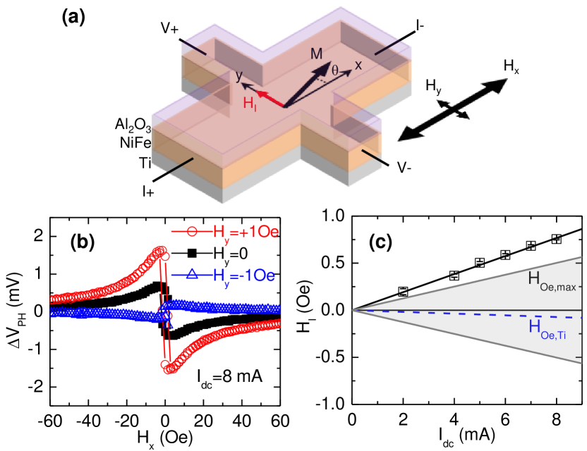
We first examine the current-induced field in a trilayer of Ti(1.2 nm)/NiFe(2.5 nm)/Al2O3(1.5 nm) by using the second-order planar Hall effect (PHE) voltage technique devised by Fan et al. Fan2013 ; Fan2014 . As illustrated in Fig. 1(a), a dc current along the x-axis generates a planar Hall voltage along the y-axis in a 100-m wide Hall bar, which is placed in the center of a two-axis Helmholtz coil. The second-order planar Hall voltage is measured while sweeping the external field (Fig. 1(b)). The total current-induced in-plane transverse field (which includes the Oersted field) pulls the magnetization away from the x-axis at an angle . When is sufficiently large (10 Oe), is small and is proportional to Fan2013 . Following the procedure in Ref. (11), we apply a constant transverse bias field Oe (Fig. 1(a),(b)) and extrapolate the critical required to cancel , i.e., to null the spectrum. For the data in Fig. 1(b), =-0.75 Oe would null , so = 0.75 Oe at = 8 mA.
As shown in Fig. 1(c), scales linearly with with slope d/d = 0.095 Oe per mA. To estimate the Oersted field contribution to , the current is assumed to be uniform within each conductive layer, such that the Oersted field comes only from the current in the Ti layer, , where is the fraction of in Ti and is the Hall bar width. The sheet resistances 2000 /sq for Ti(1.2 nm) and 350 /sq for NiFe(2.5 nm), found from four-point resistance measurements, yield = 0.15 and Oe per mA. The net is therefore an order of magnitude larger than , and moreover, the direction of opposes .
The actual Oersted field may deviate from because of nonuniform current distribution within each conductive layer and interfacial scattering, both of which are difficult to quantify. However, we can place the upper bound on the Oersted field, , by assuming that the entire flows above or below the magnetic layer. In Fig. 1(c), we shade the range bounded by . The magnitude of still exceeds , confirming the presence of an additional current-induced field with a component collinear with the Oersted field.

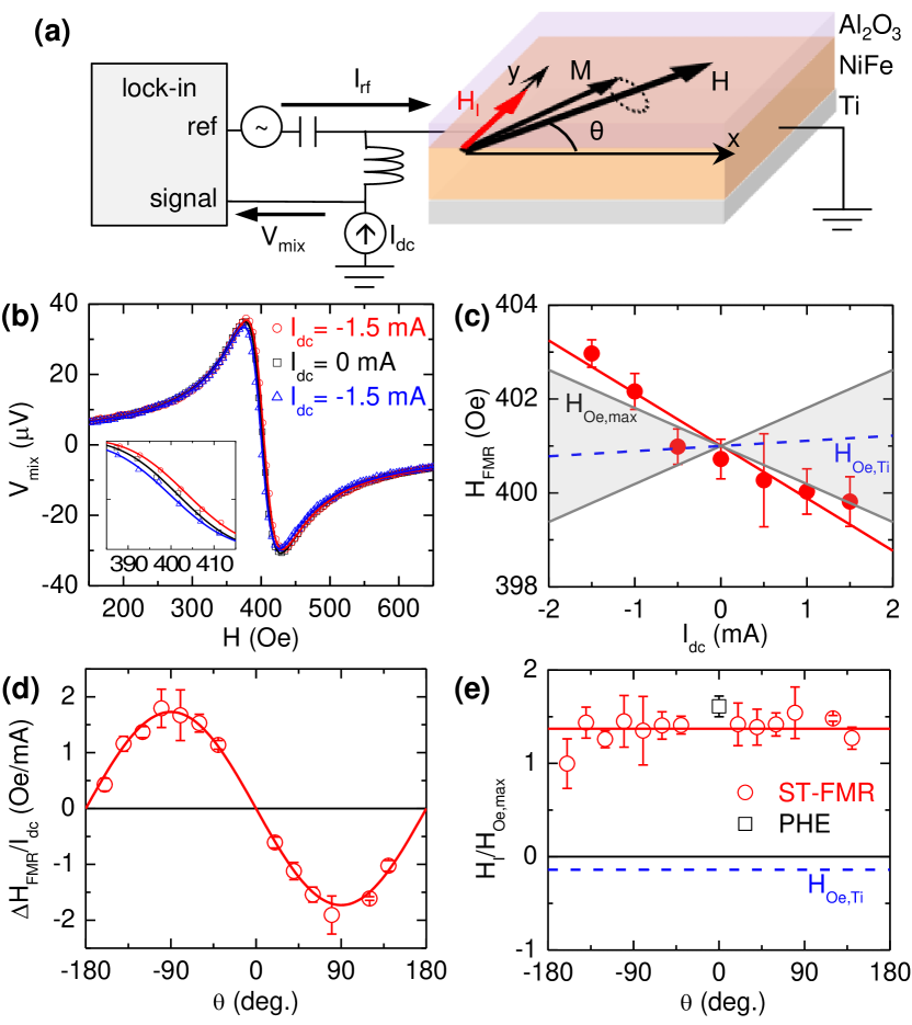
We also measure with a technique based on spin-torque ferromagnetic resonance (ST-FMR) Liu2011 ; Fang2011 . As illustrated in Fig. 2(a), the rf excitation current is injected into a 5-m wide, 25-m long strip through a ground-signal-ground electrode. While the in-plane external field is swept at an in-plane angle , the rectified mixing voltage across the strip is acquired with a lock-in amplifier. The resulting spectrum is well fit to a Lorentzian curve consisting of the symmetric component and antisymmetric component , where is the resonance linewidth and is the resonance field. We inject a small dc bias current 2 mA to measure the shift in caused by the net -induced field (31). Although the scatter in the ST-FMR data is greater than the PHE data (Fig. 1(c)), Fig. 2(c) shows that the observed shift in is significantly larger than (and opposes) the contribution from , and its magnitude exceeds the maximum possible shift from .
Fig. 2(d) shows the -induced shift as a function of in-plane magnetization angle, equal to the applied field angle for the soft NiFe layer. This angular dependence is well described by a relation, which implies that is transverse to the current axis. Fig. 2(e) shows that the constant indeed agrees well with the PHE data measured at . This finding confirms that , including the non-Oersted contribution, is entirely transverse to the current and is independent of the magnetization orientation.
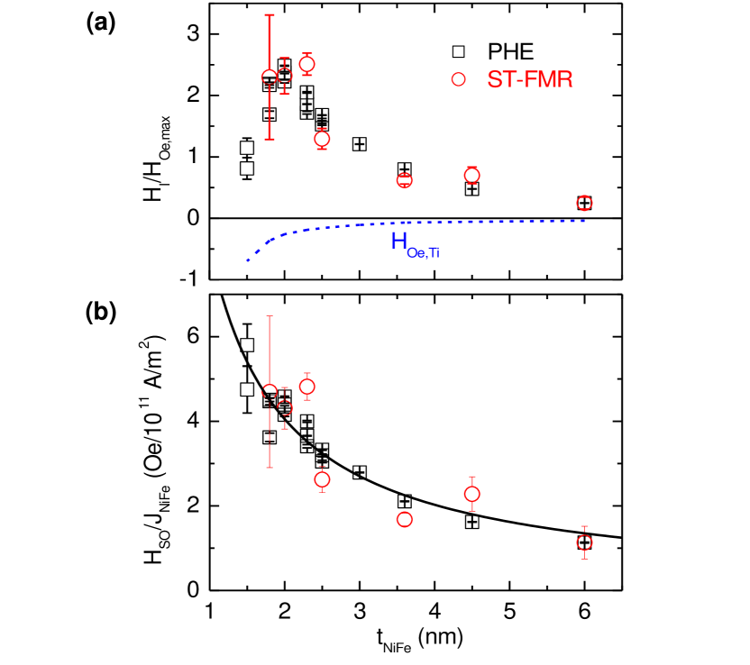
For a wide range of NiFe thickness , as shown in Fig. 3(a), we observe that cannot be accounted for by the Oersted field alone. The observed opposes in all samples, and is more than a factor of 2 larger than at nm. The drop in for nm is caused by the increasing magnitude of , as NiFe becomes more resistive and a larger fraction of current flows through Ti with decreasing .
The anomalous portion of , which cannot be explained by the classical Oersted field, may be due to a spin-orbit torque that acts as a “spin-orbit field” . In Fig. 3(b), we plot the estimated normalized by the current density in NiFe, . This normalized scales inversely with , implying that the source of is outside or at a surface of the NiFe layer. Therefore, does not arise from spin-orbit effects within the bulk of NiFe Taniguchi2015 , i.e., the reciprocal of the recently reported inverse spin-Hall effect in FMs Miao2013 ; Tsukahara2014 ; Azevedo2014 ; Wang2014e . Moreover, any possible spin-orbit toques arising from the bulk of NiFe would depend on the magnetization orientation Taniguchi2015 and are thus incompatible with the observed symmetry of (Fig. 2(e)). It is unlikely that is generated by the spin-Hall effect in Ti, because its spin-Hall angle is small (0.001) Du2014b ; Uchida2014a and only a small fraction of is expected to be in the resistive ultrathin Ti layer. In Ti/NiFe/Al2O3, we also do not observe a damping-like torque that would be expected to arise from the spin-Hall effect Haney2013a ; Freimuth2014 ; the linewidth is invariant with within our experimental resolution 0.2 Oe/mA Nan2015a .

With spin-orbit effects in the bulk of NiFe and Ti ruled out as mechanisms behind , the only known mechanism that agrees with the observed is the Rashba-Edelstein effect Edelstein1990 ; Manchon2008 ; Gambardella2011a : an interfacial spin accumulation (polarized transverse to the current) exchange couples to the magnetization in NiFe. Indeed, tight-binding Rashba model calculations reveal a field-like torque, but no damping-like torque, in the first order of spin-orbit coupling due to transverse spin accumulation independent of the magnetization orientation Kalitsov2016 .
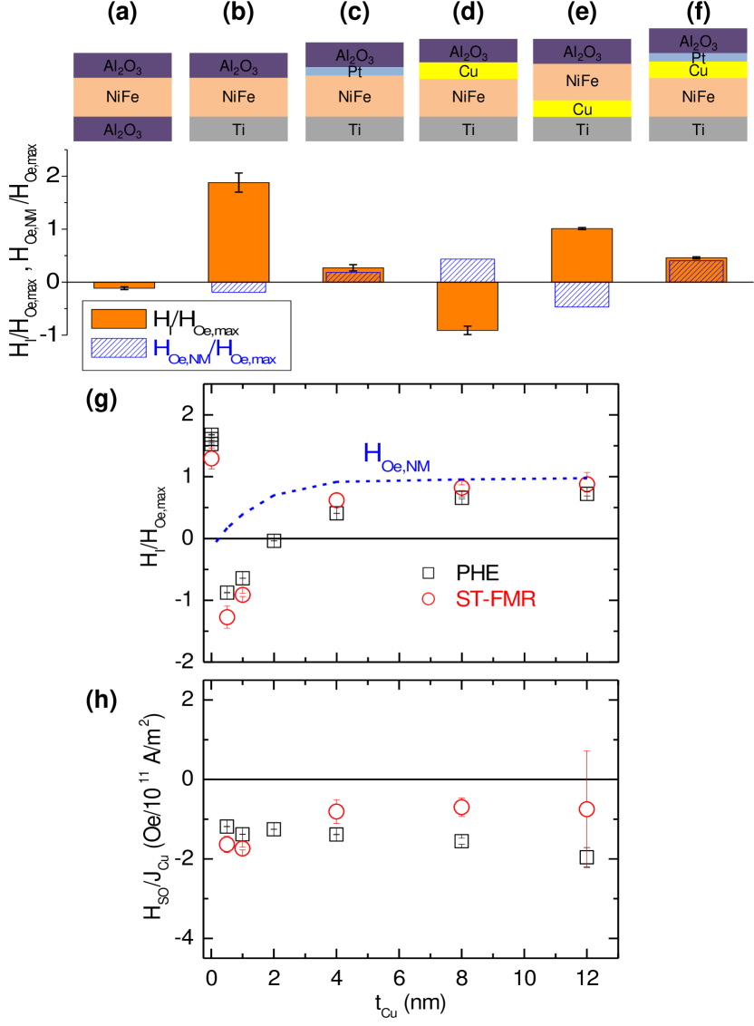
We now gain further insight into the origin of by examining its dependence on the layer stack structure, as summarized in Fig. 4(a-f). In the symmetric Al2O3(1.5 nm)/NiFe(2.3 nm)/Al2O3(1.5 nm) trilayer (Fig. 4(a)), vanishes, which is as expected because the Oersted field should be nearly zero and the two nominally identical interfaces sandwiching NiFe produces no net spin accumulation. Breaking structural inversion symmetry with the Ti(1.2 nm) seed layer results in an uncompensated interfacial spin accumulation that generates a finite (Fig. 4(b)).
Inserting Pt(0.5 nm) between the NiFe and Al2O3 layers suppresses , such that the estimated Oersted field from the nonmagnetic Ti and Pt layers entirely accounts for (Fig. 4(c)). This may seem counterintuitive since Pt exhibits strong spin-orbit coupling and a large Rashba-Edelstein effect may be expected at the Pt surface Zhang2014 . However, Pt is also a strong spin scatterer, as evidenced by an increase in the Gilbert damping parameter from 0.013 for Ti/NiFe/Al2O3 to 0.03 for Ti/NiFe/Pt/Al2O3. The accumulated spins may quickly become scattered by Pt, such that there is no net field-like torque mediated by exchange coupling Manchon2008 ; Gambardella2011a between these spins and the magnetization in NiFe. Based on the suppression of by Pt insertion, we infer that the Rashba-Edelstein effect at the NiFe/Al2O3 interface is the source of .
Inserting Cu(1 nm) at the NiFe/Al2O3 interface reverses the direction of (Fig. 4(d)). We deduce a Rashba-Edelstein effect (opposite in sign to that of NiFe/Al2O3) at the Cu/Al2O3 interface, rather than the NiFe/Cu interface, because (1) if NiFe/Cu generates the reversed , we should see an enhanced for NiFe sandwiched between Cu (bottom) and Al2O3 (top), but this is not the case (Fig. 4(e)); and (2) inserting a spin-scattering layer of Pt(0.5 nm) between Cu and Al2O3 suppresses (Fig. 4(f)).

Fig. 4(g) plots the dependence of on Cu thickness . In the limit of large (10 nm), approaches that is predominantly due to the current in the highly conductive Cu layer. From the estimated current distribution, we obtain normalized by the current density in the Cu layer, . As shown in Fig. 4(h), 1-2 Oe/1011 A/m2 exhibits little dependence on . This is consistent with the Rashba-Edelstein effect at the Cu/Al2O3 interface that is present irrespective of . Persistence of even at large implies a nonlocal Rashba-Edelstein field: the spin accumulation at the Cu/Al2O3 interface couples to the magnetization in NiFe across the Cu layer. However, further studies are required to elucidate the mechanism involving Cu, since we do not observe any apparent oscillation in with that would be expected for exchange coupling across Cu Parkin1991 .
At nm, vanishes because and compensate each other (Fig. 4(g)). Fan et al. also show near vanishing of in NiFe(2 nm)/Cu()/SOi2(3.5 nm) at nm Fan2013 , and Avci et al. report a current-induced field in Co(2.5 nm)/Cu(6 nm)/AlOx(1 nm) that is well below the estimated Oersted field Avci2014 . In each of these studies Fan2013 ; Avci2014 , a spin-orbit field due to the Rashba-Edelstein effect at the Cu/oxide interface may have counteracted the Oersted field.
In summary, we have shown a current-induced spin-orbit torque due to Rashba-Edelstein effects at NiFe/Al2O3 and Cu/Al2O3 interfaces.
This torque is distinct from previously reported spin-orbit torques because it arises even without spin-orbit coupling in the bulk of the constituent materials.
The origin of this torque is purely interfacial spin-orbit coupling, which likely emerges from the electric dipoles that develop at the metal/insulator interfaces Xu2012 ; Ibrahim2016 .
This mechanism is supported by recent theoretical predictions of current-induced spin polarization at metal/insulator interfaces in the absence of bulk spin-orbit coupling Wang2013c ; Borge2014 .
Rashba-Edelstein effects at metal/insulator interfaces may be universal and should motivate the use of various previously-neglected materials as model systems for interfacial spin-dependent physics and as components for enhancing spin-orbit torques, perhaps combined with gate-voltage tuning Liu2014b ; Emori2014c ; Bauer2015 .
One possibility is to apply interfacial band alignment techniques, similar to those for semiconductor heterostructures Kroemer2001 , to engineer giant dipole-induced Rashba-Edelstein effects.
This work was supported by the AFRL through contract FA8650-14-C-5706, the W.M. Keck Foundation, and the NSF TANMS ERC Award 1160504.
X-ray reflectivity was performed in CMSE at MIT, and lithography was performed in the George J. Kostas Nanoscale Technology and Manufacturing Research Center.
We thank Geoffrey Beach, Carl Boone, Xin Fan, Adrian Feiguin, Chi-Feng Pai, and Kohei Ueda for helpful discussions.
We give special thanks to Mairbek Chshiev, Sergey Nikolaev, and Noriyuki Sato for their comments and sharing of unpublished results.
References
- (1) V. Edelstein, Solid State Commun. 73, 233 (1990).
- (2) A. Hoffmann, IEEE Trans. Magn. 49, 5172 (2013).
- (3) J. Sinova, S. O. Valenzuela, J. Wunderlich, C. H. Back, and T. Jungwirth, Rev. Mod. Phys. 87, 1213 (2015).
- (4) A. Manchon and S. Zhang, Phys. Rev. B 78, 212405 (2008).
- (5) P. Gambardella and I. M. Miron, Philos. Trans. A. Math. Phys. Eng. Sci. 369, 3175 (2011).
- (6) P. M. Haney, H.-W. Lee, K.-J. Lee, A. Manchon, and M. D. Stiles, Phys. Rev. B 87, 174411 (2013).
- (7) A. Brataas and K. M. D. Hals, Nat. Nanotechnol. 9, 86 (2014).
- (8) A. Chernyshov, M. Overby, X. Liu, J. K. Furdyna, Y. Lyanda-Geller, and L. P. Rokhinson, Nat. Phys. 5, 656 (2009).
- (9) L. Liu, O. J. Lee, T. J. Gudmundsen, D. C. Ralph, and R. A. Buhrman, Phys. Rev. Lett. 109, 096602 (2012).
- (10) X. Fan, J. Wu, Y. Chen, M. J. Jerry, H. Zhang, and J. Q. Xiao, Nat. Commun. 4, 1799 (2013).
- (11) X. Fan, H. Celik, J. Wu, C. Ni, K.-J. Lee, V. O. Lorenz, and J. Q. Xiao, Nat. Commun. 5, 3042 (2014).
- (12) C.-F. Pai, M.-H. Nguyen, C. Belvin, L. H. Vilela-Leão, D. C. Ralph, and R. A. Buhrman, Appl. Phys. Lett. 104, 082407 (2014).
- (13) I. M. Miron, K. Garello, G. Gaudin, P.-J. Zermatten, M. V. Costache, S. Auffret, S. Bandiera, B. Rodmacq, A. Schuhl, and P. Gambardella, Nature 476, 189 (2011).
- (14) T. D. Skinner, M. Wang, A. T. Hindmarch, A. W. Rushforth, A. C. Irvine, D. Heiss, H. Kurebayashi, and A. J. Ferguson, Appl. Phys. Lett. 104, 062401 (2014).
- (15) M. Kawaguchi, T. Moriyama, T. Koyama, D. Chiba, and T. Ono, J. Appl. Phys. 117, 17C730 (2015).
- (16) G. Allen, S. Manipatruni, D. E. Nikonov, M. Doczy, and I. A. Young, Phys. Rev. B 91, 144412 (2015).
- (17) K. Garello, I. M. Miron, C. O. Avci, F. Freimuth, Y. Mokrousov, S. Blügel, S. Auffret, O. Boulle, G. Gaudin, and P. Gambardella, Nat. Nanotechnol. 8, 587 (2013).
- (18) J. Kim, J. Sinha, M. Hayashi, M. Yamanouchi, S. Fukami, T. Suzuki, S. Mitani, and H. Ohno, Nat. Mater. 12, 240 (2013).
- (19) C. O. Avci, K. Garello, M. Gabureac, A. Ghosh, A. Fuhrer, S. F. Alvarado, and P. Gambardella, Phys. Rev. B 90, 224427 (2014).
- (20) R. H. Liu, W. L. Lim, and S. Urazhdin, Phys. Rev. B 89, 220409 (2014).
- (21) S. Emori, U. Bauer, S. Woo, and G. S. D. Beach, Appl. Phys. Lett. 105, 222401 (2014).
- (22) X. Qiu, K. Narayanapillai, Y. Wu, P. Deorani, D.-H. Yang, W.-S. Noh, J.-H. Park, K.-J. Lee, H.-W. Lee, and H. Yang, Nat. Nanotechnol. 10, 333 (2015).
- (23) M. Akyol, G. Yu, J. G. Alzate, P. Upadhyaya, X. Li, K. L. Wong, A. Ekicibil, P. Khalili Amiri, and K. L. Wang, Appl. Phys. Lett. 106, 162409 (2015).
- (24) N. Sato, A. El-Ghazaly, R. M. White, and S. X. Wang, to be pubished IEEE. Trans. Magn. (2016).
- (25) K. Chen and S. Zhang, Phys. Rev. Lett. 114, 126602 (2015).
- (26) W. Zhang, M. B. Jungfleisch, W. Jiang, Y. Liu, J. E. Pearson, S. G. E. te Velthuis, A. Hoffmann, F. Freimuth, and Y. Mokrousov, Phys. Rev. B 91, 115316 (2015).
- (27) L. Xu and S. Zhang, J. Appl. Phys. 111, 07C501 (2012).
- (28) F. Ibrahim, H. X. Yang, A. Hallal, B. Dieny, and M. Chshiev, Phys. Rev. B 93, 014429 (2016).
- (29) L. Liu, T. Moriyama, D. C. Ralph, and R. A. Buhrman, Phys. Rev. Lett. 106, 036601 (2011).
- (30) D. Fang, H. Kurebayashi, J. Wunderlich, K. Výborný, L. P. Zârbo, R. P. Campion, A. Casiraghi, B. L. Gallagher, T. Jungwirth, and A. J. Ferguson, Nat. Nanotechnol. 6, 413 (2011).
- (31) T. Nan, S. Emori, C. T. Boone, X. Wang, T. M. Oxholm, J. G. Jones, B. M. Howe, G. J. Brown, and N. X. Sun, Phys. Rev. B 91, 214416 (2015).
- (32) T. Taniguchi, J. Grollier, and M. D. Stiles, Phys. Rev. Appl. 3, 044001 (2015).
- (33) B. F. Miao, S. Y. Huang, D. Qu, and C. L. Chien, Phys. Rev. Lett. 111, 066602 (2013).
- (34) A. Tsukahara, Y. Ando, Y. Kitamura, H. Emoto, E. Shikoh, M. P. Delmo, T. Shinjo, and M. Shiraishi, Phys. Rev. B 89, 235317 (2014).
- (35) A. Azevedo, O. Alves Santos, R. O. Cunha, R. Rodríguez-Suárez, and S. M. Rezende, Appl. Phys. Lett. 104, 152408 (2014).
- (36) H. Wang, C. Du, P. Chris Hammel, and F. Yang, Appl. Phys. Lett. 104, 202405 (2014).
- (37) C. Du, H. Wang, F. Yang, and P. C. Hammel, Phys. Rev. B 90, 140407 (2014).
- (38) K. Uchida, M. Ishida, T. Kikkawa, A. Kirihara, T. Murakami, and E. Saitoh, J. Phys. Condens. Matter 26, 343202 (2014).
- (39) F. Freimuth, S. Blügel, and Y. Mokrousov, Phys. Rev. B 90, 174423 (2014).
- (40) A. Kalitsov, S. A. Nikolaev, J. Velev, W. H. Butler, M. Chshiev, and O. Mryasov, unpublished (2016).
- (41) H. J. Zhang, S. Yamamoto, Y. Fukaya, M. Maekawa, H. Li, A. Kawasuso, T. Seki, E. Saitoh, and K. Takanashi, Sci. Rep. 4 (2014).
- (42) S. S. P. Parkin, Phys. Rev. Lett. 67, 3598 (1991).
- (43) X. Wang, J. Xiao, A. Manchon, and S. Maekawa, Phys. Rev. B 87, 081407 (2013).
- (44) J. Borge, C. Gorini, G. Vignale, and R. Raimondi, Phys. Rev. B 89, 245443 (2014).
- (45) U. Bauer, L. Yao, A. J. Tan, P. Agrawal, S. Emori, H. L. Tuller, S. van Dijken, and G. S. D. Beach, Nat. Mater. 14, 174 (2015).
- (46) H. Kroemer, Rev. Mod. Phys. 73, 783 (2001).