Quantum Mechanical Modeling of Nanoscale Light Emitting Diodes
Abstract
Understanding of the electroluminescence (EL) mechanism in optoelectronic devices is important for further optimization of their efficiency and effectiveness. Here, a quantum mechanical approach is formulated for modeling EL processes in nanoscale light emitting diodes (LED). Based on nonequilibrium Green’s function quantum transport equations, interactions with electromagnetic vacuum environment is included to describe electrically driven light emission in the devices. Numerical studies of a silicon nanowire LED device are presented. EL spectra of the nanowire device under different bias voltages are simulated and, more importantly, propagation and polarization of emitted photon can be determined using the current approach.
Electroluminescence (EL) is an important phenomenon employed in light emitting diode (LED) technology where light is emitted from a solid state material in response to an electrical power source. Much work has been devoted to the development of LED technology that has led to continuous advancements in both efficiencies and optical power. Schubert et al. (2005) New efforts are now directed to exploit semiconductor nanostructures that exhibit extraordinary optical and electronic properties. A more ambitious use of nanostructure devices is to exploit quantum effects which fundamentally change the mechanism of electrical-to-optical power conversion. These devices are made possible with the continuous development of nanofabrication techniques and are emerging as promising candidates for optoelectronic and energy devices. Indeed, electrically driven light emission has been reported from single carbon nanotube and nanowire Mueller et al. (2010); Huang and Lieber (2004); Bao et al. (2006); Minot et al. (2007), monolayer transition metal dichalcogenides Sundaram et al. (2013); Ross et al. (2014) and, to the ultimate miniaturization limit, from a single molecule. Marquardt et al. (2010); Reecht et al. (2014)
Understanding the EL mechanism in nanoscale LED devices is crucial to further advance the technology for more efficient lighting and enhanced communications. From the theoretical perspective, accurate description of the electrical-to-optical conversion processes is a challenging task, since the system is in nonequilibrium state driven by optical and electric field. In this context, atomic level modeling is becoming increasingly relevant, not only for accurate description of the coupled optical-electrical processes, but also to cope with the myriad of architectures and chemical compositions in modern devices. Prevailing works evaluate performance of LED devices based on classical models, relying on parmeters obtained either from experiments Kim et al. (2007); Malliaras and Scott (1999) or first-principles calculations. Kordt et al. (2015) However, these models fail to capture quantum phenomena and break down at nanoscale. For microscopic systems, light emission has been studied using Fermi’s golden rule (FGR) to evaluate transition rates between energy levels. Driel et al. (2005); Tian et al. (2011); Shiri et al. (2012) The first attempt to include quantum effects to simulate directly EL process was made by Galperin et al. for model systems. Galperin and Nitzan (2005, 2012) Recently, a diagrammatic approach is formulated to study EL in molecular junctions. Harbola et al. (2014); Goswami et al. (2015) In this letter, we present a quantum mechanical method for realistic LED device simulations. EL spectra of nanoscale devices under different bias conditions can be simulated. In addition, the method offers the possibility of analyzing the polarization of emitted light.
Quantum transport approaches based on nonequilibrium Green’s function (NEGF) method provide an efficient and versatile way to describe the coupled optical-electrical processes in nanoscale devices. Henrickson (2002); Zhang et al. (2014); Meng et al. (2015); Yam et al. (2015) Based on the Keldysh NEGF approach, steady state current can be obtained from Meir and Wingreen (1992)
| (1) |
where are lesser and greater Green’s functions, providing information on the energy states and population statistics for electrons and holes, respectively. are the self-energies and corresponds to a particular scattering process. Considering a two-terminal LED device, the scattering processes arise from the contacts and also electron-photon interaction. The first and second terms in square bracket of Eq. (1) are interpreted respectively as the incoming and outgoing rate of electrons in device due to the scattering processes. Thus, gives the steady state current resulting from different scattering processes.
The self-energy associated to the contacts can be obtained following standard procedure, Xue et al. (2002) whereas the explicit evaluation of electron-photon self-energy, requires many body diagrammatic technique and its self-consistent Born Approximation (SCBA) expression is given by Frederiksen et al. (2007); Zhang et al. (2013)
| (2) | |||||
where is photon occupation number and is photon frequency. refers to photon mode characterized by its wave vector and polarization directions . The three vectors are mutually perpendicular with each other and are defined as
| (3) |
For EL processes, the associated self-energy accounts for interactions with electromagnetic field modes in their vacuum state ( = 0). The system then undergoes spontaneous emission by relaxation to a lower energy state. for spontaneous emission is thus given by
| (4) |
Here, is electron-photon coupling matrix and its elements are given by Henrickson (2002); Zhang et al. (2014)
| (5) |
Here, is reduced Planck constant; is vacuum permittivity; is volume. The infinite sum in Eq. (2) is tranformed to integration
| (6) |
where and are defined as angle-dispersed self-energies for the two perpendicular polarization directions,
| (7) | |||||
| (8) | |||||
and
| (9) |
and . The Green’s function in Eq. (1) can then be obtained from the Keldysh equation
| (10) |
where and are retarded and advanced Green’s functions.
Substituting Eq. (6) into Eq. (1), in Eq. (1) should be zero since number of electrons should be conserved during emission of photons. Thus, the first term in Eq. (1) corresponds to transition of electron from energy level to while emitting a photon with energy . And the emission flux for photon frequency can be obtained by
| (11) |
More importantly, the wave vector and polarization of emitted photons can be determined by substituting the angle-dispersed self-energies Eqs. (7) and (8) into Eq. (11).
| (12) |
FGR has been commonly used to evaluate rate of spontaneous emissions. For simple two-level systems, Eq. (11) recovers FGR rate expresson for electron transition between the levels. It is important to emphasize that the current approach offers the possibility to determine the polarization of emitted photons and describe the nonequilibrium statistics of the device due to the bias voltage and interactions with photons.
We apply the method to model a nanoscale LED device based on a Si nanowire with cross section diameter of 1.5 nm. The nanowire is 9.5 nm in length oriented in [110] direction. Atomistic model is employed in current study which contains 1000 atoms. To form a - junction, Ga and As atoms are explicitly doped in the system to give a doping concentration of about . The surface of nanowire is passivated with hydrogen atoms to eliminate dangling bonds. The device is connected to two semi-infinite doped Si leads where external bias voltage is applied. The electronic structure of the model is described at the density functional tight-binding (DFTB) level. Porezag et al. (1995); Elstner et al. (1998) At equilibrium, an internal built-in voltage of 2.44 V is formed across the two different doped regions. The simulations are performed at 300 K.
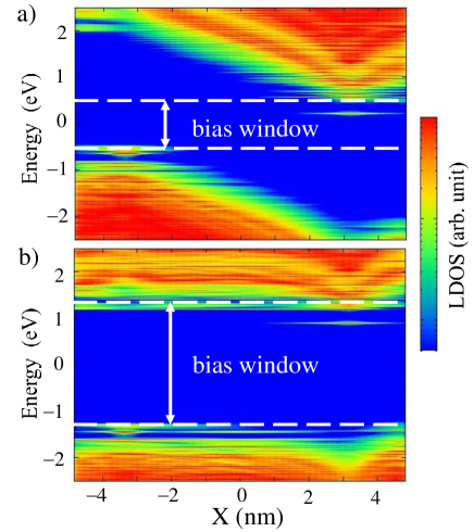
We solve Eq. (11) to obtain EL spectra of the nanowire device under different external bias voltage. In this work, the lowest order expansion to the self-energy is employed. Physically, this corresponds to the situation where density of states (DOS) of the device is unaffected by electron-photon interaction. This can be justified by the fact that interaction with electromagnetic vacuum environment is weak. Therefore, electronic structure remains intact and nonlinear effects are neglected. Fig. 1 plots the local density of states (LDOS) of the device along the wire direction for forward bias voltages of (a) 1.0 V and (b) 2.6 V. Clearly, a built-in voltage is formed across the junction, as shown in Fig. 1(a). Due to this potential barrier, electrons are localized at the -doped region while holes are localized at the -doped region. The electron-hole recombination is inhibited and the emission process is suppressed in this case. When the forward bias is increased, the potential difference across the junction is reduced. As shown in Fig. 1(b), conducting channels are formed at conduction band and valence band edges for electrons and holes, respectively. The carriers can then move along the channels driven by the external bias voltage. Due to their spatial proximity, the electron-hole pairs undergo a recombination and energy is emitted in form of photons.
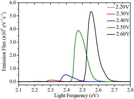
EL spectra of the nanowire LED device is plotted in Fig. 2 for different bias voltage. A single broad emission peak is observed corresponding to transitions from conduction band to valence band. This is in contrast to that of molecular junctions Goswami et al. (2015) where multiple peaks are observed due to molecular resonances. The shape of emission peak is asymmetric with tail at higher energy side due to the Fermi-Dirac distribution of charge carriers. We note that the intensity of photon emission in general increases with applied bias voltage. For bias voltage below 2.0 V, no light emission is observed. This is consistent with the results shown in the LDOS, where electron-hole recombination is suppressed when applied bias voltage is lower than the internal built-in voltage of the device. As the forward bias approaches flat band position, electrons and holes are injected simultaneously from electrodes and recombine at the junction where they meet. The emission intensity therefore increases substantially when the applied bias exceeds the built-in potential of the system, as shown in Fig. 2. For bias volatge of 2.6 V, a strong EL peak at light frequency of 2.55 eV is observed. In general, charge carriers relax nonradiatively as they pass through the device and results in near band edge emission. The system studied in this work is small compared to the coherence length. Lu et al. (2005) Electron-phonon interactions are thus neglected in the simulations and inelastic scatterings are assumed to be caused only by photons. Phonon scattering can be included similarly as Eq. (2) within NEGF formalism Galperin et al. (2007); Pecchia et al. (2007); Dubi and Di Ventra (2011) and its effect on EL of nanoscale device needs further investigations.
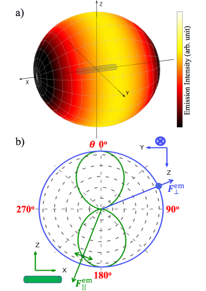
The optical emission from the nanowire LED device is further characterized by its propagation and polarization. Eq. (12) allows analysis of its spatial distribution along the two polarization vectors. Fig. 3(a) shows the EL intensity distribution of the Si LED device under bias voltage of 2.4 V. Emitted light frequency is chosen as 2.4 eV. The Si nanowire is oriented along -axis. The key features we note in Fig. 3(a) are that light is emitted mainly from surface of nanowire and essentially no edge emission is observed. We further analyse the polarization of emitted light in Fig. 3(b). The green line gives the polar plot of the emission flux in the plane while blue line plots in the plane. Here, is defined as the angle measured from -axis. represents the in-plane polarization which makes an angle with respect to the nanowire axis. As shown in Fig. 3(b), (green line) is proportional to , giving maximum EL intensity when it is aligned parallel to the nanowire axis. (blue line) represents the out-of-plane polarization and is always aligned parallel to the nanowire axis. Thus, in plane remains constant with respect to . Our results clearly show that the Si nanowire LED behaves as a linearly polarized radiation source. This is consistent with experimental observation of light emission from a carbon nanotube device. Misewich et al. (2003)
In conclusion, we formulate a quantum mechanical approach for modeling nanoscale LED devices based on NEGF quantum transport formalism. The nonequilibrium statistics in the device due to applied voltage and interactions with light are taken into account and EL processes in LED devices can be accurately described. The current approach provides the tools for determining not only the intensity but also propagation and polarization of optical emission in nanoscale devices. We demonstrate the method by simulations of EL properties of a Si nanowire LED device. Given the complexity of modern nanoscale devices, atomistic details and quantum effects are playing increasingly important roles in determining the device properties. Important also is to understand EL of single molecules in scanning tunneling microscopy experiments. Berndt et al. (1993); Wu et al. (2006) The quantum mechanical method presented in this work provides an efficient research tool for theoretical studies of coupled optical-electrical processes in these nanoscale systems.
Acknowledgements.
The authors would like to thank Wen Yang for helpful discussions. The financial support from the National Natural Science Foundation of China (21322306(C.Y.Y.), 21273186(G.H.C., C.Y.Y.)), National Basic Research Program of China (No. 2014CB921402 (C.Y.Y.)), and University Grant Council (AoE/P-04/08(G.H.C., C.Y.Y.)) is gratefully acknowledged.References
- Schubert et al. (2005) E. F. Schubert, T. Gessmann, and J. K. Kim, Light emitting diodes (Wiley Online Library, 2005).
- Mueller et al. (2010) T. Mueller, M. Kinoshita, M. Steiner, V. Perebeinos, A. A. Bol, D. B. Farmer, and P. Avouris, Nat. Nanotechnol. 5, 27 (2010).
- Huang and Lieber (2004) Y. Huang and C. Lieber, Pure Appl. Chem. 76, 2051 (2004).
- Bao et al. (2006) J. Bao, M. A. Zimmler, F. Capasso, X. Wang, and Z. F. Ren, Nano Lett. 6, 1719 (2006), pMID: 16895362.
- Minot et al. (2007) E. D. Minot, F. Kelkensberg, M. van Kouwen, J. A. van Dam, L. P. Kouwenhoven, V. Zwiller, M. T. Borgstrom, O. Wunnicke, M. A. Verheijen, and E. P. A. M. Bakkers, Nano Lett. 7, 367 (2007).
- Sundaram et al. (2013) R. S. Sundaram, M. Engel, A. Lombardo, R. Krupke, A. C. Ferrari, P. Avouris, and M. Steiner, Nano Lett. 13, 1416 (2013).
- Ross et al. (2014) J. S. Ross, P. Klement, A. M. Jones, N. J. Ghimire, J. Yan, D. G. Mandrus, T. Taniguchi, K. Watanabe, K. Kitamura, W. Yao, D. H. Cobden, and X. Xu, Nat. Nanotechol. 9, 268 (2014).
- Marquardt et al. (2010) C. W. Marquardt, S. Grunder, A. Blaszczyk, S. Dehm, F. Hennrich, H. v. Loehneysen, M. Mayor, and R. Krupke, Nat. Nanotechnol. 5, 863 (2010).
- Reecht et al. (2014) G. Reecht, F. Scheurer, V. Speisser, Y. J. Dappe, F. Mathevet, and G. Schull, Phys. Rev. Lett. 112 (2014), 10.1103/PhysRevLett.112.047403.
- Kim et al. (2007) M.-H. Kim, M. F. Schubert, Q. Dai, J. K. Kim, E. F. Schubert, J. Piprek, and Y. Park, Appl. Phys. Lett. 91 (2007), 10.1063/1.2800290.
- Malliaras and Scott (1999) G. Malliaras and J. Scott, J. Appl. Phys. 85, 7426 (1999).
- Kordt et al. (2015) P. Kordt, J. J. M. van der Holst, M. Al Helwi, W. Kowalsky, F. May, A. Badinski, C. Lennartz, and D. Andrienko, Adv. Funct. Mater. 25, 1955 (2015).
- Driel et al. (2005) A. F. V. Driel, G. Allan, C. Delerue, P. Lodahl, W. L. Vos, and D. Vanmaekelbergh, Phys. Rev. Lett. 95, 236804 (2005).
- Tian et al. (2011) G. Tian, J.-C. Liu, and Y. Luo, Phys. Rev. Lett. 106, 177401 (2011).
- Shiri et al. (2012) D. Shiri, A. Verma, C. R. Selvakumar, and M. P. Anantram, Sci. Rep. 2, 461 (2012).
- Galperin and Nitzan (2005) M. Galperin and A. Nitzan, Phys. Rev. Lett. 95 (2005), 10.1103/PhysRevLett.95.206802.
- Galperin and Nitzan (2012) M. Galperin and A. Nitzan, Phys. Chem. Chem. Phys. 14, 9421 (2012).
- Harbola et al. (2014) U. Harbola, B. K. Agarwalla, and S. Mukamel, J. Chem. Phys. 141 (2014), 10.1063/1.4892108.
- Goswami et al. (2015) H. P. Goswami, W. Hua, Y. Zhang, S. Mukamel, and U. Harbola, J. Chem. Theory Comput. 11, 4304 (2015).
- Henrickson (2002) L. E. Henrickson, J. Appl. Phys. 91, 6273 (2002).
- Zhang et al. (2014) Y. Zhang, L. Y. Meng, C. Y. Yam, and G. H. Chen, J. Phys. Chem. Lett. 5, 1272 (2014).
- Meng et al. (2015) L. Meng, C. Yam, Y. Zhang, R. Wang, and G. Chen, J. Phys. Chem. Lett. 6, 4410 (2015).
- Yam et al. (2015) C. Yam, L. Meng, Y. Zhang, and G. Chen, Chem. Soc. Rev. 44, 1763 (2015).
- Meir and Wingreen (1992) Y. Meir and N. Wingreen, Phys. Rev. Lett. 68, 2512 (1992).
- Xue et al. (2002) Y. Xue, S. Datta, and M. Ratner, Chem. Phys. 281, 151 (2002).
- Frederiksen et al. (2007) T. Frederiksen, M. Paulsson, M. Brandbyge, and A.-P. Jauho, Phys Rev. B 75 (2007), 10.1103/PhysRevB.75.205413.
- Zhang et al. (2013) Y. Zhang, C. Y. Yam, and G. H. Chen, J. Chem. Phys. 138, 164121 (2013).
- Porezag et al. (1995) D. Porezag, T. Frauenheim, T. Köhler, G. Seifert, and R. Kaschner, Phys. Rev. B 51, 12947 (1995).
- Elstner et al. (1998) M. Elstner, D. Porezag, G. Jungnickel, J. Elsner, M. Haugk, T. Frauenheim, S. Suhai, and G. Seifert, Phys. Rev. B 58, 7260 (1998).
- Lu et al. (2005) W. Lu, J. Xiang, B. Timko, Y. Wu, and C. Lieber, Proc. Natl. Acad. Sci. U.S.A. 102, 10046 (2005).
- Galperin et al. (2007) M. Galperin, M. A. Ratner, and A. Nitzan, J. Phys. Condens. Matter 19 (2007), 10.1088/0953-8984/19/10/103201.
- Pecchia et al. (2007) A. Pecchia, G. Romano, and A. Di Carlo, Phys. Rev. B 75 (2007).
- Dubi and Di Ventra (2011) Y. Dubi and M. Di Ventra, Rev. Mod. Phys. 83, 131 (2011).
- Misewich et al. (2003) J. Misewich, R. Martel, P. Avouris, J. Tsang, S. Heinze, and J. Tersoff, Science 300, 783 (2003).
- Berndt et al. (1993) R. Berndt, R. Gaisch, J. Gimzewski, B. Reihl, R. Schlittler, W. Schneider, and M. Tschudy, Science 262, 1425 (1993).
- Wu et al. (2006) S. Wu, N. Ogawa, and W. Ho, Science 312, 1362 (2006).