Tunable electronic band structures and zero-energy modes of heterosubstrate-induced graphene superlattices
Abstract
We propose a tunable electronic band gap and zero-energy modes in periodic heterosubstrate-induced graphene superlattices. Interestingly, there is an approximate linear relation between the band gap and the proportion of an inhomogeneous substrate (i.e., percentages of different components) in the proposed superlattice, and the effect of structural disorder on the relation is discussed. In an inhomogeneous substrate with equal widths, zero-energy states emerge in the form of Dirac points by using asymmetric potentials, and the positions of Dirac points are addressed analytically. Further, the Dirac point exists at only for specific potentials; every time it appears, the group velocity vanishes in the direction, and the resonance occurs. For general cases of an inhomogeneous substrate with unequal widths, part of the zero-energy states are described analytically, and differently, they are not always Dirac points. Our prediction may be realized on a heterosubstrate such as SiO2/BN.
pacs:
73.61.Wp, 73.20.At, 73.21.-bI Introduction
Since graphene was isolated in 2004 Novoselov2004 , it has attracted great attention Beenakker2008 ; Castro2009 ; Das2011 ; Goerbig2011 ; Basov2014 ; Ma2010 ; Ni2014 . Graphene is the true two-dimensional (D) material with one-atom thickness, and the D electronic gas in graphene obeys the massless Dirac equation Novoselov2005 ; Zhang2005 . In the past decade, there have been many interesting discoveries in graphene, such as the quantum anomalous Hall effect Novoselov2005 ; Purewal2006 , Klein tunneling Klein1929 ; Katsnelson2006 , plasmons Ni2015 , ballistic charge transport Miao2007 ; Du2008 , and minimum conductivity Geim2007 . Despite these exotic properties, pristine graphene is gapless in the electronic spectrum, which hinders its application in some electronic devices like transistors.
In recent years, many methods have been proposed for opening a gap in the electronic spectrum of graphene Hicks2013 ; Magda2014 ; Baringhaus2014 ; Palacio2015 ; Son2006a ; Son2006b ; Barone2006 ; Han2007 ; Li2009 ; Giovannetti2007 ; Zhou2007 ; Geim2007 ; Kim2008 ; Balog2010 ; Song2013 ; Bokdam2014 ; Jung2015 . For instance, by breaking A and B sublattice symmetry by using graphite, hexagonal boron nitride (h-BN), and SiC, gaps of meV Li2009 , meV Giovannetti2007 , and meV Zhou2007 , respectively, have already been experimentally demonstrated. Moreover, the tunable band gap and electronic properties in the monolayer heterostructure of hexagonal boron nitride and graphene (h-BNC) have been studied intensively Drost2014 ; Shinde2011 ; Zhao2012 ; Jiang2011 ; Liu2015 . One of the interesting and heuristic results in h-BNC is that the percentage of h-BN doped in the graphene layer can be used to tune the band gap Shinde2011 .
Zero-energy modes, critical states in graphene’s band structure, always lead to interesting and significant properties. Pristine graphene shows minimum conductivity and the highest shot noise at the unique Dirac point Katsnelson2006b ; Tworz2006 . It is found that the periodic potential induces new Dirac points, and resonance occurs for specific conditions Brey2009 ; Park2009 ; Barbier2010 . It is shown that confinement of the charge carriers in graphene by electrostatic potentials is possible for zero-energy states Downing2011 ; Downing2015 . Most recently, Ferreira and Mucciolo studied vacancy-induced zero-energy modes in graphene, and they proved that the early field-theoretical picture for the BD\@slowromancapi@ class BDI is valid well beyond its controlled weak-coupling regime Ferreira2015 . Further important progress reported recently is that the presence of Majorana zero-energy modes is predicted in graphene/superconductor junctions San-Jose2015 .
Inspired by these studies, our motivation here is to study the electronic band structure of heterosubstrate-induced graphene superlattices (GSLs), which refer to the GSLs with periodically modulating substrates via the BN (or SiC, graphite) and SiO2 substrates. It is known that the behavior of electrons in graphene may be different on different substrates; thus it is expected that the electronic properties in such heterosubstrate-induced GSLs can be tunable. It would be useful to mention that such heterosubstrate-induced GSLs could be fabricated technically by many advanced growth methods in electronics, like those in Refs. Tsu2005, ; Meyer2008, ; Marchini2007, ; Coraux2008, .
In this paper, we present a theory of tunable electronic band structures and zero-energy modes in the heterosubstrate-induced GSLs. It is interesting to see that the electronic band gap of such heterosubstrate-induced GSLs is dependent on the width ratio of different substrates. More importantly, this paper further shows further shows that there exist zero-energy states in such heterosubstrate-induced GSLs, which may be controlled by applying unsymmetrical square potentials. These results are compared with those in the gapless GSLsBrey2009 ; Park2009 ; Barbier2010 ; Wang2010 ; Ma2012 and the gapped GSLs Wang2011 . The properties of the electronic transport such as the conductivity and the Fano factor are discussed in detail. The possible realization of our results in experiment is also suggested.
The outline of this paper is as follows. In Sec. II, we introduce our model and method for calculating band structures, electronic transmission, conductivity, and the Fano factor. In Sec. III, we show the properties with different parameters and discuss the effect of lattice constants and structural disorder on the band gap. Afterward, we investigate the appearance of zero-energy states, the group velocities, and the resonances near zero energy. Finally, in Sec. IV, we summarize our results and draw our conclusions.
II Model and formula
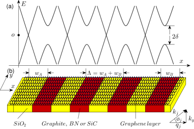
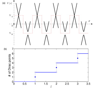
In this model, gapless and gapped graphene are periodically hybridized, such as that shown in Fig. 1. The gapless graphene is fabricated on the SiO2 substrates, and the gapped graphene is grown on the h-BN substrates Kindermann2012 ; Giovannetti2007 . The difference between gapless and gapped graphene is whether an electronic band gap caused by the sublattice symmetry breaking exists. In gapless graphene, there is a famous linear band structure with a unique Dirac point, whereas, in gapped graphene, a -wide band gap near zero energy exists.
We assume the length of these cells along the direction is infinite, and we call such a periodic superlattice, shown in Fig. 1, a heterosubstrate-induced GSL. is the width of the gapped-graphene subcell on the SiO2 substrates, is the width of the gapped-graphene subcells on BN/SiC substrates, and is the lattice constant of the whole periodic structure.
For both gapless and gapped monolayer graphene, the charge carrier near the point can be universally described by the Hamiltonian
| (1) |
where m/s is the Fermi velocity, , and , , and are Pauli matrices; is the two-component momentum operator, is the one-dimensional (D) square potential depending on the direction, is a unit matrix, and is the half width of the band gap opened by the sublattice symmetry breaking. When , the Hamiltonian (1) describes gapless graphene. The Hamiltonian acts on the two-component pseudospin wave function , where and are the smooth envelope functions for two triangular sublattices in monolayer graphene and can be written as due to the translation invariance. The solution of the eigen-equation leads to the transfer matrix Wang2010 ; Ma2012
| (2) |
which connects the wave functions at and inside the th potential. Here in Eq. (2),
is the component of the wave vector inside the th potential,
,
,
,
and the wave vector inside the potential can be expressed as
,
where .
is regarded as the transporting angle in the th region, and it should be noted that the angle is not always a
real number because the evanescent mode exists. In the case of , Eq. (2) is replaced by Wang2011
| (3) |
where . When , Eq. (2) is replaced by Wang2011
| (4) |
where . The above results are also valid for gapless graphene when .
For an infinite periodic system , with , the symbols and denote gapless and gapped graphene with square potentials and , respectively. The wave function of this periodic system is the Bloch wave function. Therefore the electronic dispersion relation is governed by
| (5) |
where is the component of the Bloch wave vector in the whole system and is the lattice constant labeled in Fig. 1(b). If has a real solution, there is an electron (hole) state in the band structure; otherwise, there is a band gap. For general cases of (i.e., ), substituting Eq. (2) into Eq. (5), we have
| (6) | |||||
Equation (6) will be used to find zero-energy modes and band structures in the next section. Here has been used.
Next, we discuss the wave function, the transmission probability, the conductivity, and the Fano factor (ratio of the shot-noise power and the current) for a finite periodic-potential system, which are a reflection of the band structure for infinite periodic systems. From the continuity of both wave functions and , the electronic transmission and reflection amplitudes can be obtained by Wang2011
| (7) |
where is the incident (exit) angle and is the element of , which is the entire transfer matrix from the incident to exit edge. We assume ; thus . Two components of the electronic wave function are expressed by Wang2010
where is the incident wave packet of the electron at and is the element of the matrix .
With the transmission probability , the conductance and the Fano factor for a given energy can be obtained by Buttiker1993 ; Masir2010
| (9) |
where all degeneracies are included. The conductivity is , where is the length of the graphene stripe in the direction.
III Result and discussion
Now, let us use the above equations to calculate the electronic band structures and the properties of transport for different situations. We would like to point out that the edge effect between gapless and gapped graphene can be neglected when the widths and are sufficiently larger than the sublattice size of graphene.
III.1 Electronic band structures
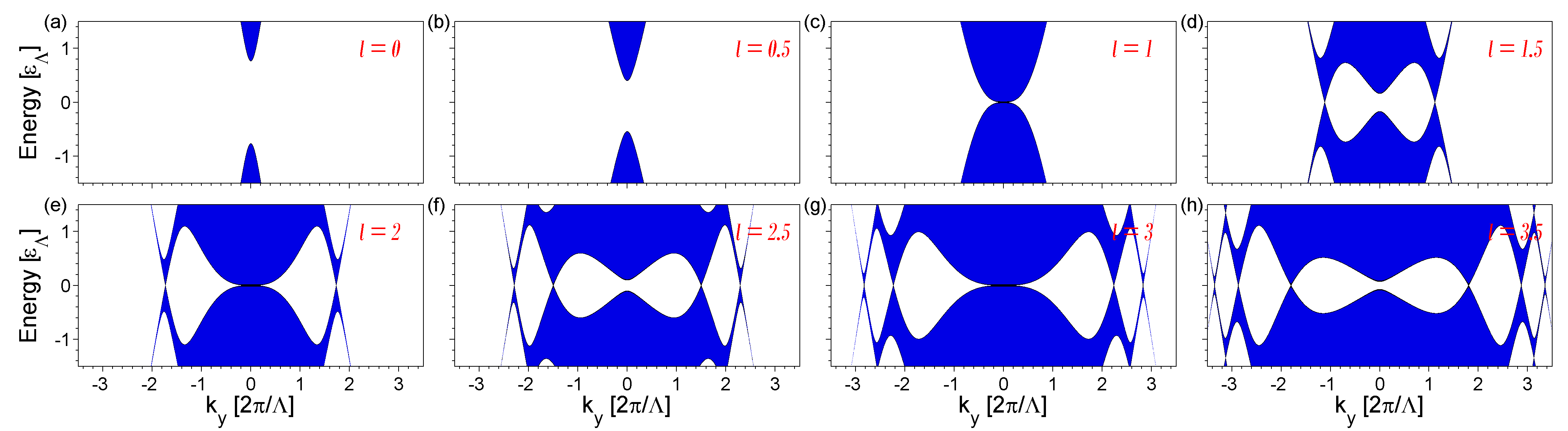
From Eq. (5), we can obtain the electronic band structures for the infinite periodic systems. Now, we let , then , and is the proportion of gapless graphene over the whole structure. For convenience, the energy is in units of , and the transverse wave vector is in units of .
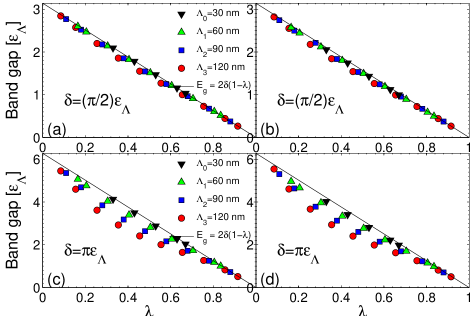
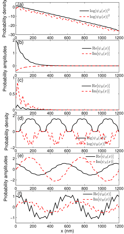
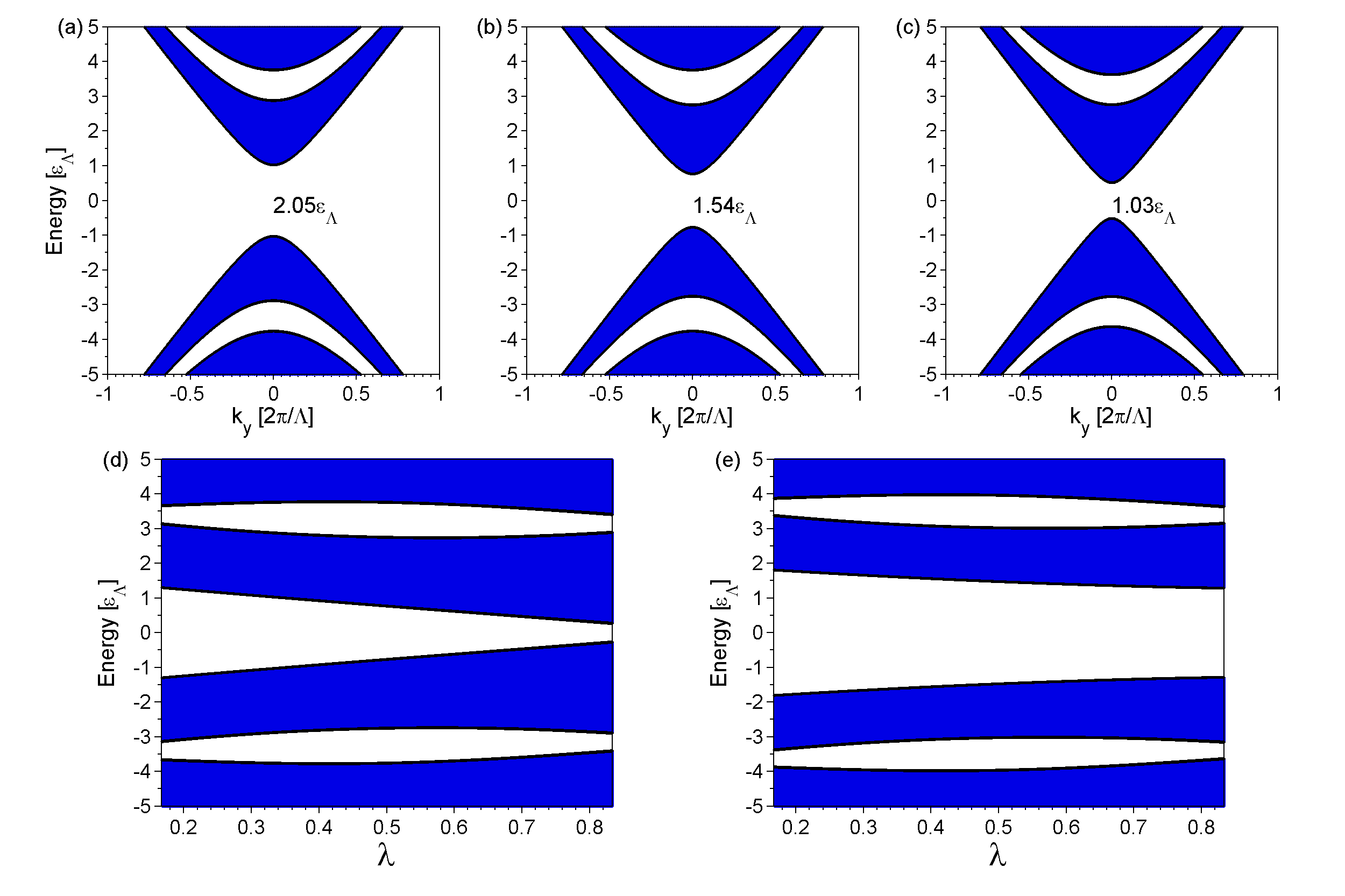
Figure 2 shows the band gap around the Fermi level for different . In Figs. 2(a)-2(c), with a fixed lattice constant, the width of the band gap near the Fermi level changes from to to with from to to . Figures 2(d) and 2(e), with and (in units of ), respectively, show that the top of the valence band (the bottom of the conduction band) increases (decreases) almost linearly as increases, and the band gap for is larger than that of the normal case (). The gap around the Fermi level completely opens compared with the symmetric forbidden bands in the valence band and conduction band [see Figs. 2(a)-2(c)], and the center position of the gap is robust against both the proportion [see Figs. 2(a)-2(e)] and the lattice constant (not shown). To find the relation between the width of the band gap and , we plot the band gap’s width versus in Fig. 3. In Figs. 3(a) and 3(c), it is shown that the relations between and can be approximately described by the linear function . Additionally, both larger and larger widen the deviation. In Figs. 3(b) and 3(d), we plot the band gap versus under the structural disorder. We consider a finite periodic structure with a width deviation of nm. From Figs. 3(b) and 3(d), we can find that the relations are robust against the structural disorder. Early works focus on the band gap of graphene nanoribbons (GNRs). In contrast, the band gap of a GNR scales inversely with the channel width Son2006a ; Barone2006 , and it has been proved by experiment Han2007 . Results similar to those in GNRs are also observed in silicene nanoribbons Song2010 .

Now, we try to qualitatively describe the scaling law of band gaps by introducing competition between propagating and decaying waves in the whole system. It is obvious that electronic energy , interaction potential , and proportions of inhomogeneous substrate all affect the competition. Higher () impairs (strengthens) the effect of the decaying wave and strengthens (impairs) the effect of the propagating wave; a larger proportion of gapped graphene also strengthens the effect of the decaying wave and, accordingly, impairs the effect of the propagating wave. In Fig. 3, with fixed , the scaling law of the band gap versus is almost linear, which may indicate that the impacts of and on the competition are almost equal. When , the impact of higher on the competition becomes stronger than the impact of ; hence the band gap is located under the linear scaling law. Specifically, we illustrate the evolutions of a decaying-dominated wave and a propagating-dominated wave in Figs. 4(a)-(c) and 4(d)-(f), respectively. With fixed , , and [see Figs. 4(a)-4(c)], both the transmission probability and amplitude decay quickly as increases, which results in no electronic state in the band structure, as shown in Fig. 2(a). In contrast, changing to [see Fig. 4(d)-4(f)] results in a propagating wave called the Bloch wave in the whole system. Using Eq. (6), we find that the Bloch wave vector in the direction is about nm-1, and the corresponding -component wavelength is nm, which is surely that pictured in Figs. 4(d)-4(f); thus there is an electronic state in the band structure for in Fig. 2(c).
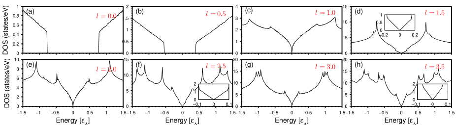
In addition, we can quantitatively verify the scaling law of the band gap by the density of states (DOS), which is plotted in Fig. 5. The DOS for the superlattice system is given by
| (10) |
where is the unit-cell area in the superlattice system. In numerical methods, we substitute a Gaussian for the function to compensate for the discrete and . Figures 5(a)-5(d) explicitly show that the DOS is zero in the gap determined by the scaling law for different .

Through Eq. (II) and the equation , we can obtain the conductivity and the Fano factor for the finite periodic system. Figure 6 shows the transmission probability, the conductivity, and the Fano factor versus the electronic energy with different . The cases with , , and correspond to the cases in Figs. 2(a)-2(c), respectively, and and separately correspond to uniform gapped graphene and uniform gapless graphene. It is seen that in the band gap, the conductivity tends to be zero, and the corresponding Fano factor tends to be the integer . For pure gapless graphene, i.e., , the conductivity exhibits the minimum at the Dirac point, and the corresponding Fano factor takes the maximum Katsnelson2006b ; Tworz2006 . We also notice that outside the band gap, as the absolute value of energy increases, the conductivity will increase almost linearly with small oscillations due to the propagating modes in the finite structures. The additional forbidden band leads to the reduction of the conductivity, which can be checked around the energy in Figs. 2(a)-2(c) and 6(b). The corresponding Fano factor gradually changes from 1 to a small value (about ). This indicates that the transport becomes ballistic.
The above discussions are under the condition of ; nevertheless, the gate voltage can change the band gap originally around the Fermi level to the position of . For unequal and , a stable gap in the band structure will also exist zk . It will be discussed further in the next section.
III.2 Zero-energy modes
In this part, we start with Eq. (6) to find zero modes. We discuss the simple and typical case of equal widths of inhomogeneous substrate in detail, i.e., , so that . Assuming , in the energy range , we have and . When in particular, Eq. (6) becomes
| (11) |

In this case, (as and ), , and ; therefore the right-hand side of Eq. (11) is larger than the integer unless , where is a positive integer. For the general cases of , there is no real solution for . These conditions lead to a gap that is located around the energy satisfying . If , is the only possible solution. Based on the above analysis and to find zero-energy states, we assume and ; thus we have . From and , we obtain
| (12) |
From , we have
| (13) |
Here denotes the serial number of a Dirac point, which will be explained later. For convenience, we assume , and Eq. (13) becomes the concise form
| (14) |
We have for propagating modes; thus and satisfy ; meanwhile, remember that .
Differently, for other cases, i.e., , to find zero-energy states located at , we should consider the conditions Wang2010 [ is the wave vector in the A (B) regions] and (), which lead to
| (15) |
and
| (16) |
with the definition of . To find zero-energy states at , we still use to determine the potentials, and we have with ( is an arbitrary positive number). Then we assume and , where and are both positive integers. From the hypotheses, we have
| (17) |
If , there will be a new zero-energy state at . For , it is difficult to find zero-energy states from Eq. (6) using the analytic method; therefore the results stated above are always a convenient approach since the zero-average wave-number gap was found zk . In addition, we emphasize that the above solutions for the cases of are not all the solutions for zero-energy states satisfying , and other unsolved zero-energy states will cluster together with the states we have gotten; hence the obtained solutions are not always Dirac points, which is very different from the case of .
We continue to discuss the case of . Figures 7(b) and 8(a)-8(h) demonstrate the evolution of the Dirac point versus for . Here can represent , as scales linearly with . The value of and Eq. (14) determine the number and the positions of the Dirac points. As increases, Dirac points move away from , and the Dirac points are generated one by one from [see Figs. 8(a)-8(h)]. If , there is no solution for , which means no Dirac points [see Figs. 7(b), 8(a), and 8(b)]. If is a positive integer, a new Dirac point is generated at [see Figs. 7(b), 8(c), 8(e), and 8(g)]. If moves forward from a positive integer, a new pair of Dirac points is generated from ; meanwhile, the Dirac point originally at vanishes, which results in an even number of Dirac points [see Figs. 7(b), 8(d), 8(f), and 8(h)]. With fixed , has possible values , and a larger denotes a Dirac point or pair of points that is closer to or appears later (consider that Dirac point moves away from as grows). For example [see Fig. 8(g)], with fixed , denotes the outermost pair of Dirac points from , denotes the outer pair of Dirac points from , and denotes the Dirac point which is exactly located at . This property is used in Fig. 9 to indicate different Dirac points. Except for creating more Dirac points by increasing and for fixed , we can achieve a similar result by increasing for fixed and . In Eq. (13), if we increase , we will get more reasonable solutions of , i.e., more Dirac points appearing. Under this condition, still must be a positive integer.
We plot the DOS in Figs. 10(a)-10(h), which correspond to Figs. 8(a)-8(h), respectively. When zero-energy modes do not exist, as in Figs. 8(a) and 8(b), the DOS is zero around zero energy. As for cases with , zero-energy modes emerge. Nevertheless, the relations between the DOS and the energy are different for different near zero energy. If is a positive integer, as in Figs. 10(c), 10(e), and 10(g), a more or less curvilinear rise in the DOS versus the energy can be observed. For the other cases, i.e., Figs. 10(d), 10(f), and 10(h), the DOS increases linearly. The linear relation between the DOS and the energy is formed because of the extra linearlike Dirac cones around zero energy, although these extra linearlike Dirac cones may be anisotropic. At each Dirac point, the group velocity becomes zero in a few directions; therefore there is no Van Hove singularity at zero energy.

Inspired by the work on the group velocity at the Dirac point of pristine graphene Park2009 ; Barbier2010 ; Park2008 , now we discuss that in this structure, which helps us to understand the resonance in Fig. 11. Group velocities in the and directions can be given by
| (18) |
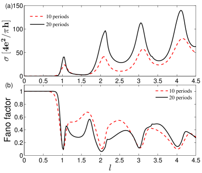
where and are the momenta in the and directions in terms of the Bloch wave. It is not convenient to find the analytical solution of Eq. (18) from Eq. (6); therefore we present the result in Fig. 9 numerically. As stated previously, the Dirac point at exists only when is a positive integer. Figure 9 shows that every time it appears, and . When the Dirac point at vanishes, as increases, the corresponding of the new pair of Dirac points gradually reduces to zero from approximately , and gradually approaches from zero. The cases with , and are shown in Fig. 9; as can be seen, they all have similar characters.
The DOS, the conductivity, and the Fano factor at zero energy are shown in Fig. 11. Brey and Fertig have found conductance resonance in the uniform gapless graphene with the periodic cosine-type potential Brey2009 ; here we observe a similar property as well. From Fig. 11, it can be seen that there are peaks in the conductivity and valleys in the Fano factor when are positive integers, and small values (about 0.1) of the Fano factor suggest the resonance at zero energy. The resonance may be caused by the appearance of the Dirac point at and its zero group velocity along the direction, as the new Dirac point and the character of lead to the strong enhancement of the DOS near zero energy [see Fig. 11(a)]. It can also be seen intuitively from Figs. 8(c), 8(e), and 8(g) that the band at (, ) becomes flat in direction, which results in the enhancement of the DOS. In addition, compared with Fig. 5(b), the conductivity versus in Fig. 11(b) has the same rising tendency if we ignore the resonance, which indicates that the potential (represented by ) enhances the conductivity by generating more Dirac points at zero energy.
Then we consider the effect of the structural disorder on the conductivity and the Fano factor at zero energy. The percentage of the largest width derivation against is up to , and we show the conductivity and the Fano factor under such structural disorder in Fig. 12. Figure 12 explicitly shows that peaks of the conductivity and valleys of the Fano factor still exist, although the shift of these peaks becomes more distinct.
Finally, in experiments, we suggest that our results could be realized on a heterosubstrate such as SiO2/BN substrate , and the conditions are that one part of the inhomogeneous substrate breaks the sublattice symmetry, which leads to a symmetry gap around the Fermi level, and another part does not. In addition, other devices which have a similar principle may be equally valid. For example, graphene with a band gap induced by patterned hydrogen adsorption Balog2010 can take the place of graphene on the BN substrate.
IV Conclusions
In summary, we investigated the band gap around the Fermi level and zero-energy modes of the electronic band structures of D graphene-based superlattices placed on the heterosubstrate with periodic square potentials.
It is found that the band gap’s width can be almost linearly tuned by the proportion of inhomogeneous substrate if equal potentials are applied on the GSLs, and the relation is robust against the effect of the structural disorder. The relation between the band gap and the proportion of an inhomogeneous substrate is exactly like comproportionation comproportionation in chemistry, which will benefit the design of graphene-based electronic devices. Moreover, the scaling law of the band gap is explained by the wave function and the DOS.
For zero-energy modes, the typical case of equal widths of an inhomogeneous substrate was discussed in detail. Although the sublattice symmetry was broken for gapped graphene, we showed that Dirac points emerge at zero energy if asymmetric potentials are applied on the GSLs, but the Dirac point at [ as ] exists only for specific potentials. Once the Dirac point at appears, the resonance occurs with the conductivity having a peak and the shot noise tending to be very low, which indicates that the transport becomes ballistic. Furthermore, we found that the resonance occurs for the strong enhancement of the DOS around zero energy, which is caused by the appearance of a Dirac point at and its zero group velocity in the direction. General cases with unequal widths of the inhomogeneous substrate were also discussed, and part of the zero-energy states was described analytically. Our prediction may be realized on a heterosubstrate such as SiO2/BN, and other devices which obey a similar principle should be equally possible.
V Acknowledgments
T.M. thanks CAEP for partial financial support. This work is supported by NSFC (Grants No. 11274275 and No. 11374034) and the National Basic Research Program of China (Grants No. 2011CBA00108 and No. 2012CB921602). We also acknowledge the support from the Fundamental Research Funds for the Center Universities under Grants No. 2015FZA3002, No. 2016FZA3004 (L.-G.W.), and No. 2014KJJCB26 (T.M.), the HSCC of Beijing Normal University, and the Special Program for Applied Research on Super Computation of the NSFC-Guangdong Joint Fund (the second phase).
References
- (1) K. S. Novoselov, A. K. Geim, S. V. Morozov, D. Jiang, Y. Zhang, S. V. Dubonos, I. V. Grigorieva, and A. A. Firsov, Science 306, 666 (2004).
- (2) C. W. J. Beenakker, Rev. Mod. Phys. 80, 1337 (2008).
- (3) A. H. Castro Neto, F. Guinea, N. M. R. Peres, K. S. Novoselov, and A. K. Geim, Rev. Mod. Phys. 81, 109 (2009).
- (4) S. Das Sarma, S. Adam, E. H. Hwang, and E. Rossi, Rev. Mod. Phys. 83, 407 (2011).
- (5) M. O. Goerbig, Rev. Mod. Phys. 83, 1193 (2011).
- (6) D. N. Basov, M. M. Fogler, A. Lanzara, F. Wang, and Y. Zhang, Rev. Mod. Phys. 86, 959 (2014).
- (7) T. Ma, F. M. Hu, Z. B. Huang, and H.-Q. Lin, Appl. Phys. Lett. 97, 112504 (2010); F. M. Hu, T. Ma, H.-Q. Lin, and J. E. Gubernatis, Phys. Rev. B 84, 075414 (2011);S. Cheng, J. Yu, T. Ma, and N. M. R. Peres, 91, 075410 (2015).
- (8) G.-X. Ni, H.-Z. Yang, W. Ji, S.-J. Baeck, C.-T. Toh, J. H. Ahn, V. M. Pereira, and B. özyilmaz, Adv. Mater. 26, 1081 (2014).
- (9) Y. Zhang, J. W. Tan, H. L. Stormer, and P. Kim, Nature (London) 438, 201 (2005).
- (10) K. S. Novoselov, A. K. Geim, S. V. Morozov, D. Jiang, M. I. Katsnelson, I. V. Grigorieva, S. V. Dubonos, and A. A. Firsov, Nature (London) 438, 197 (2005).
- (11) M. S. Purewal, Y. Zhang, and P. Kim, Phys. Status Solidi B 243, 3418 (2006).
- (12) O. Klein, Z. Phys. 53, 157 (1929).
- (13) M. I. Katsnelson, K. S. Novoselov, and A. K. Geim, Nat. Phys. 2, 620 (2006).
- (14) G.-X. Ni, H. Wang, J. S. Wu, Z. Fei, M. D. Goldflam, F. Keilmann, B.özyilmaz, A. H. Castro Neto, X. M. Xie, M. M. Fogler, and D. N. Basov, Nature Mater. 14, 1217 (2015); M. D Goldflam, G.-X. Ni, K. W Post, Z. Fei, Y. Yeo, J. Tan, A. S Rodin, B. C Chapler, B. özyilmaz, A. H Castro Neto, M. M Fogler, and D.N. Basov, Nano lett. 15, 4973 (2015).
- (15) F. Miao, S. Wijeratne, Y. Zhang, U. C. Coskun, W. Bao, and C. N. Lau, Science 317, 1530 (2007).
- (16) X. Du, I. Skachko, A. Barker, and E. Y. Andrei, Nat. Nanotechnol. 3, 491 (2008).
- (17) A. K. Geim and K. S. Novoselov, Nature Mater. 6, 183 (2007).
- (18) J. Hicks, A. Tejeda, A. Taleb-Ibrahimi, M. S. Nevius, F. Wang, K. Shepperd, J. Palmer, F. Bertran, P. Le Fèvre, J. Kunc, W. A. de Heer, C. Berger, and E. H. Conrad, Nat. Phys. 9, 49 (2013).
- (19) G. Z. Magda, X. Jin, I. Hagymási, P. Vancsó, Z. Osváth, P. Nemes-Incze, C. Hwang, L. P. Biró, and L. Tapasztó, Nature (London) 514, 608 (2014).
- (20) J. Baringhaus, M. Ruan, F. Edler, A. Tejeda, M. Sicot, A. Taleb-Ibrahimi, A.-P. Li, Z. Jiang, E. H. Conrad, C. Berger, C. Tegenkamp, and W. A. de Heer, Nature (London) 506, 349 (2014).
- (21) I. Palacio, A. Celis, M. N. Nair, A. Gloter, A. Zobelli, M. Sicot, D. Malterre, M. S. Nevius, W. A. de Heer, C. Berger, E. H. Conrad, A. T.-Ibrahimi, and A. Tejeda, Nano Lett. 15, 182 (2015).
- (22) Y. W. Son, M. L. Cohen, and S. G. Louie, Phys. Rev. Lett. 97, 216803 (2006).
- (23) Y. W. Son, M. L. Cohen, and S. G. Louie, Nature (London) 444, 347 (2006).
- (24) V. Barone, O. Hod, and G. E. Scuseria, Nano Lett. 6, 2748 (2006).
- (25) M. Y. Han, B. Özyilmaz, Y. Zhang, and P, Kim, Phys. Rev. Lett. 98, 206805 (2007).
- (26) G. Li, A. Luican, and E. Y. Andrei, Phys. Rev. Lett. 102, 176804 (2009).
- (27) G. Giovannetti, P. A. Khomyakov, G. Brocks, P. J. Kelly, and J. Van den Brink, Phys. Rev. B 76, 073103 (2007).
- (28) S. Y. Zhou, G.-H. Gweon A. V. Fedorov, P. N. First, W. A. De Heer, D.-H. Lee, F. Guinea, A. H. Castro Neto, and A. Lanzara, Nature Mater. 6, 770 (2007).
- (29) S. Kim, J. Ihm, H. J. Choi, and Y. W. Son, Phys. Rev. Lett. 100, 176802 (2008).
- (30) R. Balog, G. Jørgensen, L. Nilsson, M. Andersen, E. Rienks, M. Bianchi, M. Fanetti, E. Lægsgaard, A. Baraldi, S. Lizzit, Z. Slizzit, Z. Sljivancanin, F. Besenbacher, B. Hammer, T. G. Pedersen, P. Hofmann, and L. Hornekær, Nature Mater. 9, 315 (2010).
- (31) J. C. W. Song, A. V. Shytov, and L. S. Levitov, Phys. Rev. Lett. 111, 266801 (2013).
- (32) M. Bokdam, T. Amlaki, and P. J. Kelly, Phys. Rev. B 89, 201404(R) (2014).
- (33) J. Jung, A. M. DaSilva, A. H. MacDonald, and S. Adam, Nat. Commun. 6, 6308 (2015).
- (34) P. P. Shinde and V. Kumar, Phys. Rev. B 84, 125401 (2011).
- (35) J.-W. Jiang, J.-S. Wang, and B.-S Wang, Appl. Phys. Lett. 99, 043103 (2011).
- (36) R. Zhao, J. Wang, M. Yang, and Z. Liu, J. Phys. Chem. C 116, 21098 (2012).
- (37) R. Drost, A. Uppstu, F. Schulz, S. K. Hämäläinen, M. Ervasti, A. Harju, and P. Liljeroth, Nano Lett. 14, 5128 (2014).
- (38) T. Gao, X. Song, H. Du, Y. Nie, Y. Chen, Q. Ji, J. Sun, Y. Yang, Y. Zhang, and Z. Liu, Nat. Commun. 6, 6835 (2015).
- (39) M. I. Katsnelson, Eur. Phys. J. B 51, 157 (2006).
- (40) J. Tworzydło, B. Trauzettel, M. Titov, A. Rycerz, and C. W. J. Beenakker, Phys. Rev. Lett. 96, 246802 (2006).
- (41) L. Brey and H. A. Fertig, Phys. Rev. Lett. 103, 046809 (2009).
- (42) C. H. Park, Y. W. Son, L. Yang, M. L. Cohen, and S. G. Louie, Phys. Rev. Lett. 103, 046808 (2009).
- (43) M. Barbier, P. Vasilopoulos, and F. M. Peeters, Phys. Rev. B 81, 075438 (2010).
- (44) C. A. Downing, D. A. Stone, and M. E. P ortnoi, Phys. Rev. B 84, 155437 (2011).
- (45) C. A. Downing, A. R. Pearce, R. J. Churchill, and M. E. P ortnoi, Phys. Rev. B 92, 165401 (2015).
- (46) BD\@slowromancapi@ class is a type of Riemannian symmetric space, and the label was given by Cartan. The label BDI is not an acronym. For more detail, one may refer to R. S. Kulkarni [Bull. Am. Math. Soc., New Ser. 2, 468 (1980)].
- (47) A. Ferreira and E. R. Mucciolo, Phys. Rev. Lett. 115, 106601 (2015).
- (48) P. San-Jose, J. L. Lado, R. Aguado, F. Guinea, and J. Fernández-Rossier, Phys. Rev. X 5, 041042 (2015).
- (49) R. Tsu, Superlattice to Nanoelectronics (Elsevier, Oxford, 2005).
- (50) J. C. Meyer, C. O. Girit, M. F. Crommie, and A. Zettl, Appl. Phys. Lett. 92, 123110 (2008).
- (51) S. Marchini, S. Günther, and J. Wintterlin, Phys. Rev. B 76, 075429 (2007).
- (52) J. Coraux, A. T. N’Diaye, C. Busse, and T. Michely, Nano Lett. 8, 565 (2008).
- (53) L.-G. Wang and S. Y. Zhu, Phys. Rev. B 81, 205444 (2010).
- (54) T. Ma, C. Liang, L.-G. Wang, and H.-Q. Lin, Appl. Phys. Lett. 100, 252402 (2012).
- (55) L.-G. Wang and X. Chen, J. Appl. Phys. 109, 033710 (2011).
- (56) M. Kindermann, B. Uchoa, and D. L. Miller, Phys. Rev. B 86, 115415 (2012). This paper dose not consider the periodic-potential GSLs structure; thus we do no comparisons with it.
- (57) M. Buttiker, J. Phys: Condens. Matter 5, 9361 (1993); T. Christen and M. Buttiker, Phys. Rev. Lett. 77, 143 (1996).
- (58) M. Ramezani Masir, P. Vasilopoulos, and F. M. Pceters, Phys. Rev. B 82, 115417 (2010).
- (59) Y.-L. Song, Y. Zhang, J.-M Zhang, and D.-B. Lu, Appl. Surf. Sci. 256, 6313 (2010).
- (60) For interest, one may see Refs. [Wang2010, -Wang2011, ]; P.-L. Zhao and X. Chen, Appl. Phys. Lett. 99, 182108 (2011). The gap tuned by unequal potentials has properties similar to those in these cases.
- (61) C.-H. Park, L. Yang, Y.-W. Son, M. L. Cohen, and S. G. Louie, Nat. Phys. 4, 213 (2008).
- (62) For the BN substrate, Ref. Giovannetti2007, shows that the Fermi level exactly locates at the center position of the gap, but for the graphite and SiC substrates, Refs. [Li2009, , Zhou2007, ] show that the Fermi level is not inside the gap; thus engeerings like doping holes are needed to move the Fermi level to the center position of the gap.
- (63) Comproportionation is a chemical reaction in which two reactants, each containing the same element but with different oxidation numbers, will form a product in which the elements involved reach the same oxidation number. For example, an element A in the oxidation states and can comproportionate to the state . In our theory, the gapped graphene and the gapless graphene can be regarded as the same element with different oxidation numbers, and the widths of their gaps can be compared to oxidation numbers; similarly, the band of the whole system will have a medium-width gap. For more details about comproportionation, see P. Muller [Pure and Appl. Chem. 66, 1077 (1994)].