Electrically controlled spin-transistor operation in helical magnetic field
Abstract
A proposal of electrically controlled spin transistor in helical magnetic field is presented. In the proposed device, the transistor action is driven by the Landau-Zener transitions that lead to a backscattering of spin polarized electrons and switching the transistor into the high-resistance state (off state). The on/off state of the transistor can be controlled by the all-electric means using Rashba spin-orbit coupling that can be tuned by the voltages applied to the side electrodes.
An application of electron spin to conventional electronic devices is the basic concept lying in the heart of spintronics.Szumniak et al. (2012); Fabian et al. (2007) The special role among the spintronic devices is played by the spin field effect transistor (spin-FET), the concept of which was proposed by Datta and Das.Datta and Das (1990) According to this ideasDatta and Das (1990) the current of spin polarized electrons is injected from the ferromagnetic source into the two-dimensional electron gas (2DEG) and is electrically detected in the ferromagnetic drain. The resistance of the transistor channel depends on the electron spin, which is controlled by the Rashba spin-orbit interaction (SOI) Bychkov and Rashba (1984) generated by the voltage applied to the gate attached close to the channel. Although the coherent manipulation of electron spin in semiconductor have been demonstrated by many experimental groups,Koo et al. (2009); Crooker et al. (2005); Appelbaum et al. (2007) the realization of the functional spin-FET still remains an experimental challenge of spintronics. This is due to the fundamental physical obstacles such as the low spin-injection efficiency from ferromagnet into semiconductor (the resistance mismatch),Schmidt et al. (2000) spin relaxation,Fabian et al. (2007) and the spread of the spin precession angles. All these effects lead to the low electrical signal in the up-to date realized spin-FET.Koo et al. (2009); Wunderlich et al. (2010); Wójcik et al. (2015a)
The current research on the spin-FET is mainly focused on two directions. First, the researchers try to overcome the physical obstacles by using the spin filters based on semiconductors.Wójcik et al. (2013, 2015a) In the very recent experiment,Chuang et al. (2015) the quantum point contacts have been used as the spin injectors and detectors and about times greater conductance oscillations have been observed as compared to the conventional spin-FET.Koo et al. (2009) The second direction involves the proposals of the new spin transistor design, different from that proposed in Ref. Datta and Das, 1990 and free of its physical restrictions.Schliemann et al. (2003); Kunihashi et al. (2012)
Such an alternative spin-transistor design has been recently described by Žutić and Lee Žutic and Lee (2012) and experimentally demonstrated by Betthausen et al. in Ref. Betthausen et al., 2012. In this approach, the spin of electron flowing through the nanostructure is subjected to the combined homogeneous and helical magnetic fields. The latter is generated by ferromagnetic stripes located above the conduction channel. The transistor action is driven by the diabatic Landau-Zener transitions Landau (1932); Zener (1932) induced by the appropriate tuning of the homogeneous magnetic field. For the suitably chosen conditions the spin polarized electrons are scattered back, which gives raise to the increase of the resistance. As shown in Refs. Saarikoski et al., 2012; Betthausen et al., 2012; Wójcik et al., 2015b, by keeping the transport in the adiabatic regime, the proposed design is robust against the scattering on defects, while in the non-adiabatic regime, the additional conductance dips emerge which result from the resonant Landau-Zener transitions. Although this spin-FETBetthausen et al. (2012) seems to be free of the above-mentioned physical obstacles, it requires the application and control of the external homogeneous magnetic field, which is difficult to be applied in the integrated circuit.
Motivated by this experiment,Betthausen et al. (2012) in the present paper, we propose the spin transistor design based on the helical magnetic field, in which the spin transistor action is generated by all-electric means without the external magnetic field. For this purpose we use the Rashba spin-orbit interaction induced by the lateral electric field between electrodes located on either side of the channel.
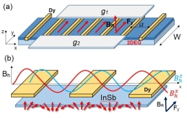
We consider the two-dimensional waveguide (nanowire) in the plane made of InSb, for which the Rashba spin-orbit coupling is reported to be strong.Nadj-Perge et al. (2012) The proposed transistor design (Fig. 1) consists of the two building blocks: (i) ferromagnetic stripes (fabricated from dysprosium, Dy) located periodically above the conduction channel, which generate the helical magnetic field in the 2DEG (this block has been realized in Ref. Betthausen et al., 2012) and (ii) two side gate electrodes ( and ), which generate the lateral electric field . The lateral electric field , controlled by the voltages applied to the side gates, induces the Rashba spin-orbit interaction with the effective magnetic field directed along the -axis. The possibility of using the SOI induced by the lateral electric field in the QPC has been recently reported in many experiments Chuang et al. (2015); Debray et al. (2009); Das et al. (2011). The change in the SOI coupling constant between the two electrodes has been obtained to be meVnm.
The Hamiltonian of the electron is given by
| (1) |
where is the conduction-band electron mass, is the momentum operator, is the identity matrix, is the vector of Pauli matrices, is the effective -factor, is the Bohr magneton, is the Rashba spin-orbit coupling constant and is the helical magnetic field, which has the form
| (2) |
where is the amplitude of the helical field, is the period of the magnetic field modulation determined by the distance between ferromagnetic stripes and is the localization of one of the ferromagnetic stripes. For simplicity, we study the waveguide with length equal to one period of the helical magnetic field modulation and . In the present paper, m.
The behavior of the electron spin in the 2DEG is determined by the superposition of the helical magnetic field generated by the ferromagnetic stripes and the Rashba effective magnetic field induced by the lateral electric field. The effective spin Zeeman energy for the parallel () and antiparallel () spin orientation (with respect to the effective magnetic field) depends on the electron position and is given by
| (3) |
where . Parameter depends on the Rashba
spin-orbit coupling , which can be tuned by changing the voltages applied to the side
electrodes.
For the suitably chosen conditions, in this two level system the diabatic Landau-Zener transitions
can take place with the probability Zener (1932); Landau (1932)
| (4) |
where . Parameter determines how fast these eigenenergies approach each other in the electron rest frame. For our system, takes on the form
| (5) |
where is the Fermi velocity.
According to Eq. (4), the probability of the Landau-Zener transitions
if the subbands crossover, i.e., the energy separation
. In Fig. 2, we present as a function
of the position in the nanowire and wave vector for two different values of .
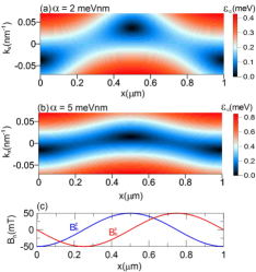
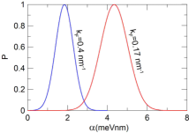
We observe that for electrons with positive wave vector, i.e., flowing from the left to the right, reaches zero for the well-defined , exactly in the middle of the waveguide, i.e. for m, for which . The value of , for which , increases with the decreasing Rashba spin-orbit coupling . Based on these results, we conclude that for the specified Fermi wave vector (Fermi energy), we can tune the Rashba coupling in order to reach the Landau-Zener transition probability . Probability as a function of is depicted in Fig. 3 for two different Fermi wave vectors. Fig. 3 shows that the maximum of the Landau-Zener transition probability shifts towards the higher value of with decreasing Fermi wave vector .
The analysis of the Landau-Zener transition probability presented above is needed to understand the spin-transistor action in the proposed spin-FET. In order to demonstrate this operation in a quantitative manner, we have performed the numerical calculations of the conductance using the scattering matrix method on the square lattice with nm.Groth et al. (2014) We have considered the electron transport for a fixed Fermi energy assuming a small bias between the leads and calculated the conductance , where the summation runs over the transmission probabilities from the subband on the input to the subband in the output channel.
In the calculations, the following values of the parameters have been used: the conduction-band electron mass in InSb, where is the free electron mass, and . We adopt the hard-wall boundary conditions in the direction assuming the width of the conduction channel nm, while the value of the helical magnetic field amplitude has been taken on the basis of the experimental report Betthausen et al. (2012) and is equal to mT.
Fig. 4 presents the conductance as a function of the Rashba spin-orbit coupling calculated for the Fermi energy meV.
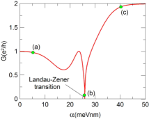
As we can see, in the presence of the spin-orbit interaction the conductance exhibits the sharp distinct dip at certain value of the spin-orbit coupling [point (b)], i.e. the device is switched into the high-resistance state. Since the changes of can be realized by the voltages applied to the side electrodes, this allows us for the full electrical control of the transistor state, i.e. the device can be switched between the high resistance (off state) and the low resistance (on state) states. The appearance of the conductance dip can be explained based on the analysis of the electron conduction subbands, which vary with position in the waveguide. The dispersion relations at the point are determined by combining the Rashba effective magnetic field generated by the lateral electric field and directed along the -axis in the entire nanostructure, and the helical magnetic field, which varies with the position. While the helical magnetic field generates the Zeeman spin splitting of the conduction subbands, the spin-orbit interaction shifts the dispersion relations in the wave vector space, in a manner that depends on the relative alignment of and . In Fig. 5, we present the lowest-energy subbands in the left lead (), in the middle of the waveguide (), where the ferromagnetic stripe is located, and in the right lead (), for different values of the spin-orbit strength marked by the points (a-c) in Fig. 4.
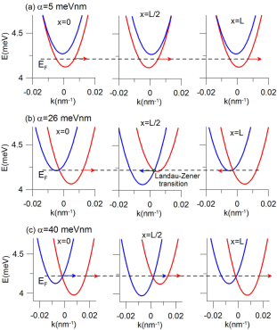
For meVnm the electrons with Fermi energy are injected into the conduction channel from the lowest-energy subband [see Fig. 5(a)]. In this case, the Rashba spin-orbit coupling is so small that the helical magnetic field is much stronger than the Rashba field . Since the Zeeman spin-splitting is only slightly affected by the spin-orbit interaction, the electrons are transmitted through the nanostructures without the scatterings giving raise to the conductance (cf. Fig. 4). For meVnm [Fig. 5(b)] a degeneracy point emerges in the middle of the waveguide, i.e., for . At this point, for the chosen Fermi energy, the Rashba field compensates the helical field and the total magnetic field vanishes. Since the distance between spin-split eigenenergies approaches zero, the Landau-Zener transmission probability . As a result the electrons are transmitted to the upper Zeeman subband [blue curve in Fig. 5 (b)]. However, the energy of this subband, for positive wave vector in the right lead is above the Fermi energy [cf. Fig. 5(b), ], which means that there are no available electronic states in the right lead. This leads to the backscattering of electrons. As a result, the transport is blocked, which gives raise to the conductance dip presented in Fig. 4. The further increase of the Rashba coupling constant causes that the energy minima of both spin-split subbands are below Fermi energy and both the subbands conduct electrons. The conductance increases up to [cf. Fig. 4, point (c)].
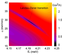
The spin-transistor action in the proposed device is generated by the Landau-Zener transitions between spin-split subbands, which occurs when the Rashba effective field compensates the helical field at some region of the nanostructure. For the fixed Fermi energy this can be realized by applying the appropriate voltages to the side gate electrodes. Nevertheless, the spin-orbit interaction strength depends not only on the electric field but also on the Fermi energy. This means that for different Fermi energies the conditions for the Landau-Zener transitions are fulfilled for different Rashba coupling constant. This dependence is depicted in Fig. 6, which presents the conductance as a function of coupling and Fermi energy . In Fig. 6, we mark the range, in which the Landau-Zener transitions occur. We see that the values of , for which the spin-transistor action is expected, decreases with the increasing Fermi energy .
In summary, we have proposed the electrically controlled spin transistor setup, which is based on the effect of the helical magnetic field generated by the ferromagnetic stripes and the lateral Rashba spin-orbit interaction with the strength tuned by the voltages applied to the side electrodes. We have shown the the appropriate tunning of the Rashba spin-orbit interaction results in the blocking of the electron transport due to the Landau-Zener transition. This allows us for the all-electric control of the device and switching it between the low-resistance (on state) to the high resistance state (off state). It is worth noting that the proposed setup combines the blocks already tested in the recent experiments: the helical magnetic field in 2DEG has been generated by the ferromagnetic stripes used in Ref. Betthausen et al., 2012, while the lateral Rashba spin-orbit interaction in the QPC has been intensively studied as potential spin filters.Debray et al. (2009); Das et al. (2011) Therefore, we expect that the proposed spin transistor can be realized in the near future.
References
- Szumniak et al. (2012) P. Szumniak, S. Bednarek, B. Partoens, and F. M. Peeters, Phys. Rev. Lett. 109, 107201 (2012).
- Fabian et al. (2007) J. Fabian, A. Matos-Abiague, C. Ertler, P. Stano, and I. Zutic, Acta Physica Slovaca 57, 565 (2007).
- Datta and Das (1990) S. Datta and B. Das, Appl. Phys. Lett. 56, 665 (1990).
- Bychkov and Rashba (1984) Y. A. Bychkov and E. I. Rashba, J. Phys. C 17, 6039 (1984).
- Koo et al. (2009) H. C. Koo, J. H. Kwon, J. Eom, J. Chang, S. H. Han, and M. Johnson, Science 325, 1515 (2009).
- Crooker et al. (2005) S. A. Crooker, M. Furis, X. Lou, C. Adelman, D. L. Smith, C. J. Palmstrøm, and P. A. Crowell, Science 309, 2191 (2005).
- Appelbaum et al. (2007) I. Appelbaum, B. Huang, and D. J. Monsma, Nature 447, 295 (2007).
- Schmidt et al. (2000) G. Schmidt, D. Ferrand, L. W. Molenkamp, A. T. Filip, and B. J. van Wees, Phys. Rev. B 62, 4790(R) (2000).
- Wunderlich et al. (2010) J. Wunderlich, P. Byong-Guk, A. C. Irvine, L. P. Zârbo, E. Rozkotová, P. Nemec, V. Novák, J. Sinova, and T. Jungwirth, Science 330, 1801 (2010).
- Wójcik et al. (2015a) P. Wójcik, J. Adamowski, M. Woloszyn, and B. J. Spisak, J. Appl. Phys. 118, 014302 (2015a).
- Wójcik et al. (2013) P. Wójcik, J. Adamowski, M. Woloszyn, and B. J. Spisak, Appl. Phys. Lett. 102, 242411 (2013).
- Chuang et al. (2015) P. Chuang, S. C. Ho, L. W. Smith, F. Sfigakis, M. Pepper, C. H. Chen, J. C. Fan, J. P. Griffiths, I. Farrer, H. E. Beere, G. A. C. Jones, and T. M. Ritchie, D A Chen, Nature Nanotechnology 10, 35 (2015).
- Schliemann et al. (2003) J. Schliemann, J. C. Egues, and D. Loss, Phys. Rev. Lett. 90, 146801 (2003).
- Kunihashi et al. (2012) Y. Kunihashi, M. Kohda, H. Sanada, H. Gotoh, T. Sogawa, and J. Nitta, Appl. Phys. Lett. 100, 113502 (2012).
- Žutic and Lee (2012) I. Žutic and J. Lee, Science 337, 1225219 (2012).
- Betthausen et al. (2012) C. Betthausen, T. Dollinger, H. Saarikoski, V. Kolkovsky, G. Karczewski, T. Wojtowicz, K. Richter, and D. Weiss, Science 337, 1221350 (2012).
- Landau (1932) L. Landau, Physics of the Soviet Union 2, 46 (1932).
- Zener (1932) C. Zener, Proc. R. Soc. Lon. 137, 696 (1932).
- Saarikoski et al. (2012) H. Saarikoski, T. Dollinger, and K. Richter, Phys. Rev. B 86, 165407 (2012).
- Wójcik et al. (2015b) P. Wójcik, J. Adamowski, M. Woloszyn, and B. J. Spisak, Semicond. Sci. Technol. 30, 6 (2015b).
- Nadj-Perge et al. (2012) S. Nadj-Perge, V. S. Pribiag, J. W. G. van den Berg, K. Zuo, S. R. Plissard, E. P. A. M. Bakkers, S. M. Frolov, and L. P. Kouwenhoven, Phys. Rev. Lett. 108, 166801 (2012).
- Debray et al. (2009) P. Debray, R. S. Rahman, S anad Newrock, M. Cahay, A. Ngo, A. T. Ulloa, S. E. Herbert, and M. Muhammad, Nature Nano Technol. 4, 759 (2009).
- Das et al. (2011) P. P. Das, K. Chetry, N. Bhandari, J. Wan, M. Cahay, R. Newrock, and S. T. Herbert, Appl. Phys. Lett. 99, 122105 (2011).
- Groth et al. (2014) C. W. Groth, M. Wimmer, A. R. Akhmerov, and X. Waintal, New J. Phys. 16, 063065 (2014).