Spin Mapping of Surface and Bulk Rashba States in Ferroelectric -GeTe(111) Films
Abstract
A comprehensive mapping of the spin polarization of the electronic bands in ferroelectric -GeTe(111) films has been performed using a time-of-flight momentum microscope equipped with an imaging spin filter that enables a simultaneous measurement of more than 10.000 data points (voxels). A Rashba type splitting of both surface and bulk bands with opposite spin helicity of the inner and outer Rashba bands is found revealing a complex spin texture at the Fermi energy. The switchable inner electric field of GeTe implies new functionalities for spintronic devices.
The strong coupling of electron momentum and spin in low-dimensional structures allows an electrically controlled spin manipulation in spintronic devices Wolf et al. (2001); Zutic et al. (2004); Maekawa (2006); Awschalom and Flatte (2007), e.g. via the Rashba effect Rashba. (1960).
The Rashba effect has first been experimentally demonstrated in semiconductor heterostructures, where an electrical field perpendicular to the layered structure, i.e. perpendicular to the electron momentum, determines the electron spin orientation relative to its momentum Datta and Das (1990); Nitta et al. (1997); Engels et al. (1997). An asymmetric interface structure causes the necessary inversion symmetry breaking and accounts for the special spin-splitting of electron states, the Rashba effect Rashba. (1960), the size of which can be tuned by the strength of the electrical field.
For most semiconducting materials the Rashba effect causes only a quite small splitting of the order of Å-1 and thus requires experiments at very low temperatures Koo et al. (2009); Wunderlich et al. (2010); Betthausen et al. (2012) and also implies large lateral dimensions for potential spintronic applications. A considerably larger splitting has been predicted theoretically Sante et al. (2013) and was recently found experimentally for the surface states of GeTe(111) Liebmann et al. (2015); Krempasky et al. (2015).
GeTe is a ferroelectric semiconductor with a Curie temperature of 700 K. Thus, besides the interface induced Rashba splitting, the ferroelectric properties also imply a broken inversion symmetry within the bulk and thus would allow for the electrical tuning of the bulk Rashba splitting via switching the ferroelectric polarization Sante et al. (2013); Dresselhaus (1955); Zhang et al. (2014). This effect is of great interest for non-volatile spin orbitronics Wunderlich et al. (2010).
For GeTe a bulk Rashba splitting of Å-1 has been predicted theoretically Sante et al. (2013). Experimentally, bulk-Rashba bands are rare and have only been found in the layered polar semiconductors BiTeCl and BiTeI Ishizaka et al. (2011); Lee et al. (2011); C.-R.Wang et al. (2013); Sakano et al. (2013) that, however, are not switchable.
A characterization of the ferroelectric properties and a measurement of the spin polarization of the surface states of GeTe(111) at selected -points has been performed previously by force microscopy Kolobov et al. (2014); Wang et al. (2014) and spin-resolved angular resolved photoemission spectroscopy, respectively Liebmann et al. (2015). A recent experimental and theoretical study revealed that at the Fermi level the hybridization of surface and bulk states causes surface-bulk resonant states resulting in unconventional spin topologies with chiral symmetry Krempasky et al. (2015).
Here, we demonstrate the spin structure of surface and bulk bands of the GeTe(111) surface using the novel photoemission technique of spin-resolved time-of-flight momentum microscopy that allows for an effective parallel spin mapping of the electronic states Schönhense et al. (2015). The previous findings for the spin texture at the Fermi level are confirmed. In addition we reveal a Rashba-type spin texture of the bulk band, too.
Single-domain epitaxial -GeTe(111) films with a thickness of 32 nm are grown by molecular beam epitaxy (MBE) on in-situ prepared Si(111) and are transferred in ultra-high vacuum (UHV) to the spin-resolved time-of-flight momentum microscope. Thus, we are able to probe the pristine surface, which shows an outward ferroelectric polarization. It was previously shown that a metastable inverted polarization state can be written using ex-situ piezo force microscopy. Details of the structural and ferroelectric properties of the samples are reported in Ref. Liebmann et al. (2015).
The photoemission experiment has been performed at the undulator beamline U125-NIM at BESSY II in the single bunch mode, providing vacuum ultraviolet photon pulses (photon energy range 15 eV to 27 eV) of 50 ps duration and a repetition rate of 1.25 GHz. The time-of-flight momentum microscope yields a simultaneous acquisition of the spectral function in the full surface Brillouin zone and several eV energy interval. Details of this instrument are given in Ref. Schönhense et al. (2015). For the present experiment the overall energy and the resolution is 86 meV and 0.03 Å-1. The photon beam shines at an incidence angle of 680 onto the surface parallel to the - direction with linear polarization with the electric field vector parallel to the plane of incidence (p-polarization). Spin detection was achieved by electron reflection at the W(100) spin filter crystal in the [010] azimuth at 450 reflection angle Kolbe et al. (2011); Kutnyakhov et al. (2015). The spin direction parallel to the - direction is probed. Two datasets , , were acquired at scattering energies 26.5 eV and 30.5 eV, respectively. At 26.5 eV the reflection asymmetry is Kutnyakhov et al. (2015) while it is negligibly small at 30.5 eV. The spin polarization is then determined by
| (1) |
where denotes the energy-dependent relative reflection coefficient as described in Ref. Tusche et al. (2013). The energy dependence of was neglected as we analyzed only a narrow energy interval of less than 1 eV.
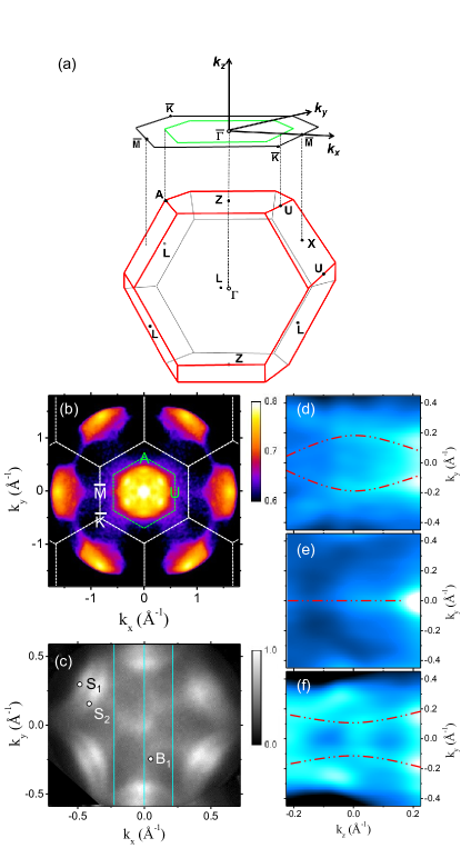
First, we describe experimental results obtained with the straight branch of the instrument without spin detection. Fig. 1(a) shows a sketch of the surface and bulk first Brillouin zone of GeTe(111). The known six-fold symmetric shape of the bulk Rashba band Sante et al. (2013) is displayed on the ZAU hexagonal surface of the bulk Brillouin zone. Fig. 1 (b) presents a constant energy slice at the Fermi level covering the complete first bulk Brillouin zone measured with a photon energy of 18.5 eV. According to Ref. Liebmann et al. (2015) eV probes the bulk bands at in the vicinity of the ZAU plane.
Fig. 1(c) shows a magnified constant energy spectrum at a binding energy eV measured at a photon energy of eV. The splitted surface Rashba bands with a six-fold symmetry a clearly resolved. Additional arcs appear revealing a three-fold symmetry. In order to proof that these arcs are bulk bands we performed the experiment for a number of photon energies from eV to eV in steps of 0.5 eV resulting in the four-dimensional dataset . Each of these sets consisting of 1250 resolved -points and 24 resolved energy-slices took about 15 minutes of acquisition time. From the data we extracted constant energy maps at a binding energy eV with fixed values and Å-1 [Figs. 1(d-f)]. Bulk bands are identified by their dispersion with for Figs. 1(d,f). The symmetric behavior of the dispersion allows the conclusion that the high symmetry point corresponds to a photon energy of 19.5 eV. Using the known radius of the Brillouin zone Å-1 and assuming an excitation into free electron states, we derive an inner potential of eV, agreeing well with theoretical values Liebmann et al. (2015). In contrast, the dispersion-less behavior of the band shown in Fig. 1(e) indicates its nature as a surface or surface-resonant band.


In the following, we discuss the spin polarization of the electronic bands measured after reflection at the W(100) spin filter crystal probing the -component . In order to remove artificial experimental asymmetries we exploit the fact that the (, Z, M)-plane represents a mirror plane of the whole experiment enforcing the condition . From the complete three-dimensional map we present constant energy slices at selected binding energies in Fig. 2(a-g). Each slice integrates over an energy interval of 43 meV. At (Fig. 2(a) ) the spin orientation is oriented clockwise (counter-clockwise) for the outer (inner) surface Rashba band as seen from above the sample surface. The maximum value is observed at the top and bottom of the outer Rashba surface band. The left and right outer Rashba surface bands show a polarization of in agreement with the Rashba-type spin texture, i.e. . Spin polarization for the inner bands are of opposite direction and only slightly smaller. These results confirm previously published data Liebmann et al. (2015); Krempasky et al. (2015).
The constant energy slice at eV shown in Fig. 2(f) also reveals the spin orientation of the bulk band although the Rashba splitting is not resolved in the intensity signal. In order to emphasize the weak spin contrast we present the cuts in Fig. 3(a,b) parallel to ZA for and Å-1, the latter representing a cut through the bulk band. The spin polarization is of opposite sign to the left and right from the bulk band’s maximum intensity. The maximum spin polarization of the bulk band is considerably smaller than that of the surface bands. This can be explained by the smaller Rashba splitting and the corresponding partial overlap of the intensity of inner and outer band. A large perpendicular spin component cannot be excluded from the experiment but seems unlikely in respect to the theoretical predictions Liebmann et al. (2015); Krempasky et al. (2015). The spin direction is mostly perpendicular to the -cut shown in Figs. 3(a,b). The component for the larger absolute of the Rashba splitted band is also parallel to that of the surface band with larger value, which is in agreement with the Rashba-type spin orientation, respective the theoretical predictions for the equilibrium ferroelectric polarization of GeTe Dresselhaus (1955); Krempasky et al. (2015).
In summary, we performed a spin mapping of surface and bulk Rashba states in the complete surface and bulk Brillouin zone of ferroelectric -GeTe(111) films. The theoretical prediction of the Rashba splitting of bulk bands is confirmed. The spin helicity is in line with the prediction for the equilibrium outwards electrical polarization of GeTe(111) connecting it to the ferroelectricity of GeTe. This represents the necessary precondition for application of this material in non-volatile spintronic devices.
The authors gratefully acknowledge financial support from the BMBF (05K13UM1, 05K13PA and 05K13WMA), Deutsche Forschungsgemeinschaft (DFG EL/18-1 within SPP1666 and SFB 917-A3), Center of INnovative Emerging MAterials (CINEMA) and Stiftung Rheinland Pfalz für Innovation (project 1038).
References
- Wolf et al. (2001) S. A. Wolf, D. D. Awschalom, R. A. Buhrmann, J. M. Daughton, S. von Molnar, M. L. Roukes, A. Y. Chtelkanova, and D. M. Treger, Science 2001 294, 1488 (2001).
- Zutic et al. (2004) I. Zutic, J. Fabian, and S. D. Sarma, Rev. Mod. Phys. 76, 323 (2004).
- Maekawa (2006) S. Maekawa, ed., Concepts in Spin Electronics (Oxford University Press, Oxford, UK, 2006).
- Awschalom and Flatte (2007) D. D. Awschalom and M. E. Flatte, Nature Phys. 3, 153 (2007).
- Rashba. (1960) E. Rashba., Sov. Phys. Solid State 2, 1109 (1960).
- Datta and Das (1990) S. Datta and B. Das, Appl. Phys. Lett. 56, 665 (1990).
- Nitta et al. (1997) J. Nitta, T. Akazaki, H. Takayanagi, and T. Enoki, Phys. Rev. Lett. 78, 1335 (1997).
- Engels et al. (1997) G. Engels, J. Lange, T. Schäpers, and H. Lüth, Phys. Rev. B 1997 55, 1958 (1997).
- Koo et al. (2009) H. C. Koo, J. H. Kwon, J. Eom, J. Chang, S. H. Han, and M. Johnson, Science 325, 1515 (2009).
- Wunderlich et al. (2010) J. Wunderlich, B. G. Park, A. C. Irvine, L. P. Zarbo, E. Rozkotova, P. Nemec, V. Novak, J. Sinova, and T. Jungwirth, Science 330, 1801 (2010).
- Betthausen et al. (2012) C. Betthausen, T. Dollinger, H. Saarikoski, V. Kolkovsky, G. Karczewski, T. Wojtowicz, K. Richter, and D. Weiss, Science 337, 324 (2012).
- Sante et al. (2013) D. D. Sante, P. Barone, R. Bertacco, and S. Picozzi, Adv. Mat. 25, 509 (2013).
- Liebmann et al. (2015) M. Liebmann, C. Rinaldi, D. D. Sante, J. Kellner, C. Pauly, R. N. Wang, J. E. Boschker, A. Giussani, S. Bertoli, M. Cantoni, L. Baldrati, I. Vobornik, G. Panaccione, D. Marchenko, J. Sanchez-Barriga, O. Rader, R. Calarco, S. Picozzi, R. Bertacco, and M. Morgenstern, Adv. Mat. , doi:10.1002/adma.201503459 (2015).
- Krempasky et al. (2015) J. Krempasky, H. Volfova, S. Muff, N. Pilet, G. Landolt, M. Radovic, M. Shi, D. Kriegner, V. Holy, J. Braun, H. Ebert, F. Bisti, V. Rogalev, V. Strocov, G. Springholz, J. Minar, and J. H. Dil, arXiv:1503.05004 (2015).
- Dresselhaus (1955) G. Dresselhaus, Phys. Rev. 100, 580 (1955).
- Zhang et al. (2014) X. Zhang, Q. Liu, J. W. Luo, A. J. Freeman, and A. Zunger, Nature Phys. 10, 387 (2014).
- Ishizaka et al. (2011) K. Ishizaka, M. S. Bahramy, H. Murakawa, M. Sakano, T. Shimojima, T. Sonobe, K. Koizumi, S. Shin, H. Miyahara, A. Kimura, K. Miyamoto, T. Okuda, H. Namatame, M. Taniguchi, R. Arita, N. Nagaosa, K. Kobayashi, Y. Murakami, R. Kumai, Y. Kaneko, Y. Onose, and Y. Tokura, Nature Mater. 10, 521 (2011).
- Lee et al. (2011) J. S. Lee, G. A. H. Schober, M. S. Bahramy, H. Murakawa, Y. Onose, R. Arita, N. Nagaosa, and Y. Tokura, Phys. Rev. Lett. 107, 117401 (2011).
- C.-R.Wang et al. (2013) C.-R.Wang, J.-C. Tung, R. Sankar, C.-T. Hsieh, Y.-Y. Chien, G. Y. Guo, F. C. Chou, and W.-L. Lee, Phys. Rev. B 88, 081104 (2013).
- Sakano et al. (2013) M. Sakano, M. S. Bahramy, A. Katayama, T. Shimojima, H. Murakawa, Y. Kaneko, W. Malaeb, S. Shin, K. Ono, S. Kumigashira, R. Arita, N. Nagaosa, H. Y. Hwang, Y. Tokura, and K. Ishizaka, Phys. Rev. Lett. 110, 107204 (2013).
- Kolobov et al. (2014) A. Kolobov, D. Kim, A. Giussani, P. Fons, J. Tominaga, R. Calarco, and A. Gruverman, Appl. Phys. Lett. Mater. 2, 066101 (2014).
- Wang et al. (2014) R. Wang, J. Boschker, E. Bruyer, D. D. Sante, S. Picozzi, K. Perumal, A. Giussani, H. Riechert, and R. Calarco, J. Phys. Chem. C 118, 29724 (2014).
- Schönhense et al. (2015) G. Schönhense, K. Medjanik, and H. Elmers, J. Electr. Spectr. Rel. Phen. 200, 94 (2015).
- Kolbe et al. (2011) M. Kolbe, P. Lushchyk, B. Petereit, H. J. Elmers, G. Schonhense, A. Oelsner, C. Tusche, and J. Kirschner, Phys. Rev. Lett. 107, 207601 (2011).
- Kutnyakhov et al. (2015) D. Kutnyakhov, H. J. Elmers, G. Schönhense, C. Tusche, S. Borek, J. Braun, J. Minar, and H. Ebert, Phys. Rev. B 91, 014416 (2015).
- Tusche et al. (2013) C. Tusche, M. Ellguth, A. Krasyuk, A. Winkelmann, D. Kutnyakhov, P. Lushchyk, K. Medjanik, G. Schönhense, and J. Kirschner, Ultramicroscopy 130, 70 (2013).