Effect of interface geometry on electron tunnelling in Al/Al2O3/Al junctions
Abstract
We investigate how different interface geometries of an Al/Al2O3 junction, a common component of modern tunnel devices, affect electron transport through the tunnel barrier. We study six distinct Al/Al2O3 interfaces which differ in stacking sequences of the metal and the oxide surface atoms and the oxide termination. To construct model potential barrier profiles for each examined geometry, we rely on first-principles density-functional theory (DFT) calculations for the barrier heights and the shapes of the interface regions as well as on experimental data for the barrier widths. We show that even tiny variations in the atomic arrangement at the interface cause significant changes in the tunnel barrier parameters and, consequently, in electron transport properties. Especially, we obtain that variations in the crucial barrier heights and widths can be as large as 2 eV and 5 Å, respectively. Finally, to gain information about the average properties of the measured junction, we fit the conductance calculated within the WKB approximation to the experimental data and interpret the fit parameters with the help of the DFT results.
pacs:
73.40.Gk, 73.40.Rw, 73.30.+yKeywords: Al/Al2O3, metal-oxide interface, electron tunnelling, tunnel barrier, band offset, thin film, MIM junction
1 Introduction
Regardless of numerous experimental and theoretical investigations of metal-oxide interfaces, very little is known about the effect of the interfacial geometry on electron transport. The issue is of paramount importance particularly for metal-insulator-metal (MIM) tunnel junctions where a thin oxide layer creates for electrons a potential barrier between two metals [1, 2]. In particular, despite the vast popularity of Al/Al2O3/Al junctions in modern nanoelectronics and continuous interest in their novel applications, for example, in qubits and Superconducting Quantum Interference Devices (SQUIDs) [3, 4, 5], single-electron transistors (SETs) [6, 7], energy storage [8], infrared sensors [9], to the best of our knowledge, not a single theoretical study about the influence of the interface geometry on electron tunnelling has been performed for these systems. The existing theoretical studies, which are based on fitting the calculated data to the measured current-voltage characteristics (-), usually employ the standard Simmons model for calculating current densities [10]. The model suggests an analytic expression for the current density applicable to any shape of the barrier given that the average barrier height and width are known or represent fit parameters. Following the general model, current-voltage relationships are also deduced for the rectangular barrier including image force effects and considering various voltage ranges.
Usually, the thickness of the realistic insulating layer varies throughout the junction. Therefore, the width of the tunnel barrier (which may differ from the physical thickness of the insulator) also varies. This is of substantial importance because the conductance of the tunnel junction is known to depend exponentially on the barrier width [11]. Non-uniformity of the order of even one atomic layer may cause significant changes in the electron transport properties of the device [1]. To address the non-uniformity in the thickness (and in the oxidation level) of the insulating layer, a double-layer barrier model has been introduced in [12]. In this model, the barrier heights and thicknesses are evaluated by fitting the numerically calculated tunnel probabilities to experimental data assuming a rectangular potential and employing Simmons model for the current density.
The second primary parameter defining the tunnelling properties, i.e., the height of the potential barrier in the junction, may be affected by the metal states penetrating into the oxide gap. Thereby, additional energy levels are introduced for the tunnelling electrons, similarly to the metal-semiconductor junctions [13]. To study the effect of such evanescent states on tunnel transport, the transfer matrix method [14] was applied in [15] together with the Simmons model to calculate - curves for rectangular and side-modified rectangular barriers. A similar method was employed in [16] with an image-force-modified tunnel barrier profile to study the impact of the substrate on electron transport in Al/Al2O3/metal junctions. Based on the Simmons model, extensive analyses of experimental data were presented in [17] and it was concluded that there is a strong correlation between the barrier height and the thickness. Additionally, a discrete distribution of barrier thicknesses with the peak-to-peak distances corresponding to a single oxygen layer was observed.
In all the above-listed studies, the main approach has been the assumption of a certain shape of the barrier, mainly rectangular with possible modifications, and the fitting of the calculated - data to the experimentally measured one in order to find the height and the width of the barrier. Although these studies provide valuable insight into the average barrier or transport properties, they lack the atomic-scale characterization. On the other hand, theoretical studies which are based on atomic modelling involve a single model geometry, leaving aside all the possible interface effects [16, 18]. The goal of this work is to establish a link between the structural properties of the interface and the corresponding barrier parameters (i.e., the height and the width). Since in theory, there is an uncountable number of options to interface the two materials, it is impossible to examine all the potential configurations. Therefore, we study by first-principles electronic structure calculations six representative geometries of the Al/Al2O3 interface to extract the barrier parameters for electron tunnelling. The chosen structures differ in stacking sequences and oxide terminations. On the basis of our first-principles results and the experimental data, we demonstrate in this paper that both the barrier height as well as the thickness are highly dependent on the atomic arrangement and the stoichiometry at the interface. In addition, by fitting the semiclassically calculated conductance to the experimental - curve and comparing the results to those obtained from the density-functional theory (DFT), we predict the average barrier parameters and the most expected geometry of the junction measured in our experiment.
2 Experimental methods
In the following, we describe the fabrication and measurement techniques. Single tunnel junctions are made by electron beam lithography and shadow evaporation technique [19]. Several Al-AlxOy-Al junctions were formed between the fingers and the common electrode. The thickness of all the fingers and the common electrode is 25 nm. The tunnel barrier (AlOx) of the junction was formed in-situ by thermal oxidation before the deposition of the second layer of Al. A close-up of two tunnel junctions is shown in the scanning-electron micrograph (SEM) together with the experimental setup in figure 1.
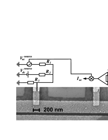
We measure the differential conductance in a liquid helium dipstick at = 4.2 K with a standard lock-in technique. The measurement setup shown in figure 1 consists of dc and ac voltage sources, low noise current preamplifier (DL instruments 1211), and a lock-in amplifier (SR 830). We obtain the differential conductance as , where is the measured ac current through the junction and the applied ac bias voltage calculated according to the voltage division. The dc voltage is .
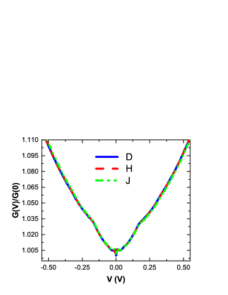
The measured differential conductance curves of three junctions are shown in figure 2 as solid blue (sample D), dashed red (sample H), and dash-dotted green (sample J). The differential conductance has a parabolic shape and a Coulomb blockade dip at zero bias voltage. Parabolic dependence is also the lowest-order result from Simmons model for tunnelling through a rectangular barrier [10]. The zero-bias conductance is determined through the parabolic fit with the - curve and is found to be 1802.17 , 1794.5 and 1765.5 for the three junctions. Coulomb blockade dip is ignored in the fitting.
3 Theoretical methods
3.1 Modelling Al/Al2O3 interfaces
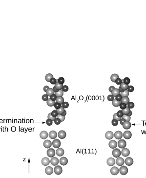
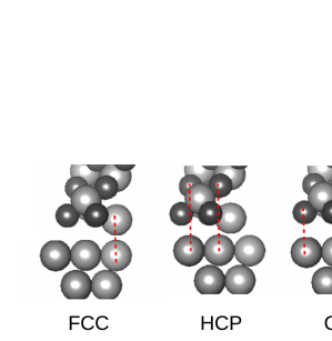
In our first-principles calculations, the model junction consists of a 5-layer substrate for the Al(111) surface and either single Al layer- or O layer-terminated oxide (figure 3). The oxide is represented as the crystalline Al2O3 having hexagonal unit cell and the (0001) surface parallel to the interface. For each termination we examine interface structures with three different stacking sequences: face-centred cubic (FCC), hexagonal closed packed (HCP) and octahedral (OT) (figure 3(b)). Thus, in total, we investigate six different structures. Throughout the paper we label the interfaces as ”1Al FCC”, etc., which read as ”single Al layer-terminated oxide with FCC stacking sequence”, etc. For example, the structures presented in figure 3(a) correspond to the O FCC and 1Al FCC interfaces. To extract barrier parameters, we first relax the chosen structures using DFT with the GPAW code [20, 21]. We carry out calculations with the 4x4x1 Monkhorst-Pack k-point grid and the PBE exchange-correlation functional [22]. The simulation box includes 5 Å vacuum on each side of the slab along the axis. To avoid the artificial electric field due to asymmetry, we apply the dipole correction to the electrostatic potential [23, 24] perpendicularly to the interface, as implemented in GPAW. Further details of the calculation setup and the procedure for selecting the interfaces, as well as a thorough discussion on their mechanical and electronic properties will be provided in a separate paper.
3.2 Extraction of barrier parameters
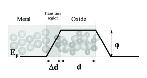
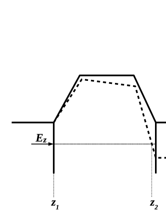
The simplest model for the profile of the tunnel barrier is a one-dimensional rectangular potential wall corresponding to an abrupt transition between the metal and the oxide. However, the importance of accounting for a transition region (along with an electron effective mass for the oxide) has been pointed out in [18]. Hence, we start by assuming a trapezoidal shape for the potential. To construct barrier profiles for our systems, we need to know the barrier heights , transition region widths and the widths of the barriers for each geometry (figure 4). In the following section, we describe the details for determining the three parameters.
3.2.1 Barrier height
The tunnel barrier height is estimated according to the Schottky model [25]:
| (1) |
where is the work function of the metal, i.e., the difference between the Fermi level () of the metal and the vacuum level, and is the electron affinity of the oxide, i.e., the difference between the conduction band minimum (CBM) of the oxide and the vacuum level. Since the definition of is based solely on the properties of the two isolated bulk materials, it neglects the effects of the interface formed between them. In particular, due to the charge transfer across the interface, a dipole barrier is exerted in this region which may be different for different interface geometries and chemical compositions. On the other hand, because of the long-range character of the Coulomb interaction the band alignment between the adjacent metal and the oxide is determined, in addition to the bulk properties, by the electronic distribution at the interface. As a consequence, to apply (1) to the interface, one needs to know the position of the oxide CBM inside the junction. Since PBE is known to underestimate band gaps, instead of using the theoretical value for CBM, it is more convenient to first find the valence band minimum (VBM) of the oxide. Next, CBM can be obtained by adding the experimental value of the oxide band gap () to the VBM found from DFT. For the experimental band gap we use a value of 8.8 eV [26]. Thus (1) is equivalent to:
| (2) |
or,
| (3) |
where VBO is the valence band offset relative to the Al Fermi level. Thus, the problem maps to finding the VBO for the interface. For this purpose we use the macroscopic average technique which was first developed for finding valence band offsets in lattice-matched metal-semiconductor heterojunctions and was further extended to the lattice-mismatched case [27, 28, 29]. According to the method the valence band offset reads as:
| (4) |
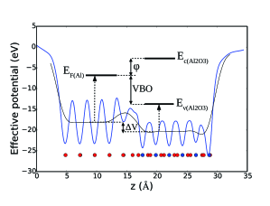
where is the band-structure term and is the potential line-up. is defined as the difference between the VBM of the oxide and the Fermi level of the metal, both measured with respect to the macroscopic average electrostatic potentials in the corresponding bulk materials. Therefore, is independent of the interface and is defined by the bulk band structure, only. In contrast, is an interface-dependent term and represents the difference between the macroscopic average electrostatic potentials in the bulk-like regions of the interfaced materials. Figure 5 illustrates the calculation procedure for the barrier heights on the example of 1Al FCC interface.
| Geometry | 1Al FCC | 1Al HCP | 1Al OT | O FCC | O HCP | O OT |
|---|---|---|---|---|---|---|
| VBO(eV) | ||||||
| (eV) | 1.15 | 3.15 | 2.65 | 1.25 | 1.25 | 1.75 |
Since the junction is lattice-mismatched and, correspondingly, the periodicity of is different in the metal and in the oxide bulk regions, the macroscopic averaging of the potential is done twice successively: first with the window size matched with the periodicity of the bulk Al, next - with the periodicity of the bulk Al2O3.
The Schottky barrier heights obtained for various interfaces are summarized in table 1. Our results show that the geometry of the interface highly influences the tunnelling properties as the difference in the barrier heights can be as large as 2 eV, against the average value of 1.87 eV. On the other hand, it is gratifying to note that the barrier heights derived based on experimental data are reported to be approximately 2 eV [16]. The barrier heights for the Al-terminated interfaces are, on average, higher than those of the O-terminated interfaces, with the mean heights being 2.32 eV and 1.42 eV, respectively. This gives rise to an about 1 eV difference between the average heights of the two different terminations.
3.2.2 Transition region width
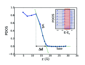
Assuming that the local density of states follows the shape of the barrier along the coordinate perpendicular to the interface [16, 18], we extract the width of the transition region between the metal and the oxide from the projected density of states (PDOS) for atomic layers at the interface. For this reason, we perform linear fittings for the base and the leg of the trapezoid separately (figure 6). The layer-projected densities of states are plotted as a function of the coordinate, and averaged over an energy window centred at the Fermi level (inset in the upper right corner).
The obtained results are summarized in table 2. Interestingly, the transition widths of both the Al- and O-terminated interfaces follow the same trend: FCC, HCP, and OT in the order of decreasing width. The significant magnitude of indicates a pronounced deviation from the square barrier assumption, where an abrupt transition between the metal and the oxide is assumed. It must be noted that the presence of the transition region lowers the average height of the zero-bias barrier by a factor of compared to the rectangular barrier, since , and at . This suggests that the barrier heights determined by fitting the rectangular barrier models (such as the widely used Simmons model [10]) with the experimental - curves should be expected, in fact, to be higher by a factor of for symmetrical barriers.
| Geometry | 1Al FCC | 1Al HCP | 1Al OT | O FCC | O HCP | O OT |
|---|---|---|---|---|---|---|
| (Å) | 5.83 | 2.78 | 2.62 | 3.34 | 3.15 | 2.05 |
3.2.3 Barrier width
The last parameter of our tunnel barrier model is the width . To analyse the experimental structures, we assume that the interface studied in the experiment is mainly composed of one of the modelled structures. For each case we fit the width with the measured zero-bias conductance. According to reference [18] the conductance through our model barrier is:
| (5) |
where
| (6) |
and
| (7) |
The above expression has been derived following the Simmons model adopted for the trapezoidal barrier profile and taking into account the contribution of the electrons to tunnelling only from the states close to the Fermi energy. We calculate the effective electron mass from the DFT band structure of the bulk oxide. Our obtained value, 0.38 , is in a perfect agreement with earlier experimental and theoretical works [30, 31]. The obtained widths are displayed in table 3.
| Geometry | 1Al FCC | 1Al HCP | 1A OT | O FCC | O HCP | O OT |
|---|---|---|---|---|---|---|
| (Å) | 8.89 | 6.77 | 7.54 | 10.34 | 10.48 | 9.70 |
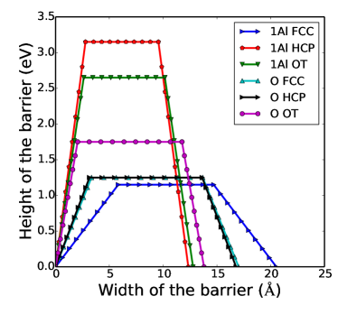
Our results demonstrate that O-terminated interfaces exhibit wider barriers compared to the Al-terminated counterparts, with average values of 7.73 Å and 10.17 Å, respectively. Based on the data in tables 1-3, resulted barrier profiles are visualized in figure 7.
4 Analysis of the experimental data
Since the widths were extracted by fitting to a single point, the zero-bias conductance, this way, we obtain the picture only about the relative widths of the different barriers with respect to each other. In addition, the electron effective mass of the oxide, which was fixed at the bulk value, might differ for each interface. Furthermore, we assumed that the interface measured in the experiment was composed of only one of the discussed interfaces, which might not be the case in the real junction. Therefore, to explain the experimental data, we extend our analyses beyond the zero bias. We make an average evaluation of the barrier parameters, and of the effective mass, using the WKB approximation by fitting the conductance to the experimental - curve. , , and are left as free parameters. The tunnel probability along the direction within the WKB approximation is calculated with the following expression:
| (8) |
And the ensuing current density is:
| (9) | |||
where is the effective electron mass, is the energy of the incident electron, and and are the classical turning points at the given energy (figure 8).
As it is shown in figure 2, the experimental curve exhibits a kink at about 0.17 V. The behaviour above this point has not been explained consistently in the existing studies, although, it has been suggested earlier to be the result of electron-phonon scattering [32]. Therefore, we consider only the bias range below 0.17 V as the WKB approximation does not account for inelastic effects. We apply a tilt in a form of a linear potential to the trapezoid as a modification caused by the bias voltage (figure 8). Unlike for a rectangle, the width of the trapezoid is now reduced due to the tilt and it is dependent on . The fitting, which reproduces essentially the parabolic - dependence, results in a barrier height of 2.56 eV, a transition region width of 1.70 Å, and a barrier width of 8.43 Å. The obtained barrier height is significantly higher than the barrier height corresponding to any O-terminated interface found from the DFT calculations. In contrast, it is closest to that of the 1Al OT configuration with the error of only 3. The second best agreement between the ab-initio and fitted values is found for the 1Al HCP configuration with the error of 18. This indicates that the measured junction (mainly) consists of the Al-terminated interfaces. However, this reasoning cannot totally exclude the presence of O-terminated interfaces. The transition region width is underestimated compared to those obtained using DFT, with the biggest errors for the 1Al FCC, O FCC and O HCP geometries. Concentrating on the Al-terminated cases, the best agreement is found, again, for the 1Al OT and 1Al HCP interfaces, what further supports our previous prediction. The fitted and the DFT values of agree by 35 and 39 for 1Al OT and 1Al HCP, respectively. Taking into account that in our first-principles calculations our model crystalline geometries are idealistic approximations to the real junction geometry, which in fact, is amorphous, we consider the agreement between the two methods rewarding.
The electron effective mass derived from fitting, 0.29 , is smaller than the calculated bulk value.
5 Summary
In conclusion, by combining first-principles density-functional and classical methods, we have extracted the tunnel barrier profiles for six possible interface geometries of the Al/Al2O3 interface. Variations in the obtained barrier heights, the barrier widths and the widths of the transition regions demonstrate that the electron transport properties of the junctions are highly sensitive specifically to the geometry of the interface. We obtained that the O-terminated interfaces exhibit on average 0.9 eV lower and 2.44 Å wider barriers compared to the Al-terminated ones. The resulted transition region widths suggest that the real barriers are better represented by the trapezoid. In addition, by fitting the semiclassical model to the experimental - curve, we have obtained information about the average barrier properties in a real junction. When compared with our DFT-based results the fitting predicts that the interfaces are Al-terminated and are best described by the octahedral stacking. The gained information is important for understanding electron transport through tunnel barriers on the atomistic level.
References
References
- [1] V. F. Maisi, O.-P. Saira, Yu. A. Pashkin, J. S. Tsai, D. V. Averin, and J. P. Pekola. Real-time observation of discrete andreev tunneling events. Phys. Rev. Lett., 106:217003, May 2011.
- [2] John M. Martinis and Megrant A. UCSB final report for the CSQ program: Review of decoherence and materials physics for superconducting qubits.
- [3] DanDan Shen, Ran Zhu, WeiWei Xu, JunJie Chang, ZhengMing Ji, GuoZhu Sun, ChunHai Cao, and Jian Chen. Character and fabrication of Al/Al2O3/Al tunnel junctions for qubit application. Chinese Science Bulletin, 57(4):409–412, 2012.
- [4] T. A. Palomaki, S. K. Dutta, Hanhee Paik, H. Xu, J. Matthews, R. M. Lewis, R. C. Ramos, K. Mitra, Philip R. Johnson, Frederick W. Strauch, A. J. Dragt, C. J. Lobb, J. R. Anderson, and F. C. Wellstood. Initializing the flux state of multiwell inductively isolated Josephson junction qubits. Phys. Rev. B, 73:014520, Jan 2006.
- [5] Michio Watanabe. Single-electron transistors in electromagnetic environments. Phys. Rev. B, 69:094509, Mar 2004.
- [6] Y. Nakamura, D. L. Klein, and J. S. Tsai. Al/Al2O3/Al single electron transistors operable up to 30 K utilizing anodization controlled miniaturization enhancement. Applied Physics Letters, 68(2), 1996.
- [7] M. Kenyon, A. Amar, D. Song, C. J. Lobb, and F. C. Wellstood. Behavior of Al-Al2O3-Al single-electron transistors from 85 mK to 5 K. Applied Physics Letters, 72(18), 1998.
- [8] F. Behzadi, M. Moradi, H.R. Karimi-Alavijeh, and A. Gharavi. The effect of anodization voltage and surface morphology on the capacitance properties of Al-Al2O3-Al nanocapacitors. Vacuum, 99:204 – 210, 2014.
- [9] Thang Duy Dao, Kai Chen, Satoshi Ishii, Akihiko Ohi, Toshihide Nabatame, Masahiro Kitajima, and Tadaaki Nagao. Infrared perfect absorbers fabricated by colloidal mask etching of Al-Al2O3-Al trilayers. ACS Photonics, 2(7):964–970, 2015.
- [10] John G. Simmons. Generalized formula for the electric tunnel effect between similar electrodes separated by a thin insulating film. Journal of Applied Physics, 34(6):1793–1803, 1963.
- [11] J. C. Fisher and I. Giaever. Tunneling through thin insulating layers. Journal of Applied Physics, 32(2), 1961.
- [12] N. Arakawa, Y. Otaka, and K. Shiiki. Evaluation of barrier height and thickness in tunneling junctions by numerical calculation on tunnel probability. Thin Solid Films, 505(1–2):67 – 70, 2006.
- [13] J. Tersoff. Schottky barrier heights and the continuum of gap states. Phys. Rev. Lett., 52:465–468, Feb 1984.
- [14] R. Tsu and L. Esaki. Tunneling in a finite superlattice. Applied Physics Letters, 22(11), 1973.
- [15] Jungmun Jung, Yongmin Kim, and Hyunsik Im. Tunneling transport simulation in asymmetric junction devices with evanescent states at a junction interface. Journal of the Korean Physical Society, 55(6):2512–2516, 2009.
- [16] Hyuntae Jung, Yongmin Kim, Kyooho Jung, Hyunsik Im, Yu. A. Pashkin, O. Astafiev, Y. Nakamura, Hosik Lee, Y. Miyamoto, and J. S. Tsai. Potential barrier modification and interface states formation in metal-oxide-metal tunnel junctions. Phys. Rev. B, 80:125413, Sep 2009.
- [17] K Gloos, P J Koppinen, and J P Pekola. Properties of native ultrathin aluminium oxide tunnel barriers. Journal of Physics: Condensed Matter, 15(10):1733, 2003.
- [18] M. Zemanová Diešková, A. Ferretti, and P. Bokes. Tunneling through Al/AlOx/Al junction: Analytical models and first-principles simulations. Phys. Rev. B, 87:195107, May 2013.
- [19] T. A. Fulton and G. J. Dolan. Observation of single-electron charging effects in small tunnel junctions. Phys. Rev. Lett., 59:109–112, Jul 1987.
- [20] J Enkovaara, C Rostgaard, J J Mortensen, J Chen, M Dułak, L Ferrighi, J Gavnholt, C Glinsvad, V Haikola, H A Hansen, H H Kristoffersen, M Kuisma, A H Larsen, L Lehtovaara, M Ljungberg, O Lopez-Acevedo, P G Moses, J Ojanen, T Olsen, V Petzold, N A Romero, J Stausholm-Møller, M Strange, G A Tritsaris, M Vanin, M Walter, B Hammer, H Häkkinen, G K H Madsen, R M Nieminen, J K Nørskov, M Puska, T T Rantala, J Schiøtz, K S Thygesen, and K W Jacobsen. Electronic structure calculations with GPAW: a real-space implementation of the projector augmented-wave method. Journal of Physics: Condensed Matter, 22(25):253202, 2010.
- [21] J. J. Mortensen, L. B. Hansen, and K. W. Jacobsen. Real-space grid implementation of the projector augmented wave method. Phys. Rev. B, 71:035109, Jan 2005.
- [22] John P. Perdew, Kieron Burke, and Matthias Ernzerhof. Generalized gradient approximation made simple. Phys. Rev. Lett., 77:3865–3868, Oct 1996.
- [23] Jörg Neugebauer and Matthias Scheffler. Adsorbate-substrate and adsorbate-adsorbate interactions of Na and K adlayers on Al(111). Phys. Rev. B, 46:16067–16080, Dec 1992.
- [24] Lennart Bengtsson. Dipole correction for surface supercell calculations. Phys. Rev. B, 59:12301–12304, May 1999.
- [25] W. Schottky. Vereinfachte und erweiterte theorie der randschicht-gleichrichter. Zeitschrift für Physik, 118(9-10):539–592, 1942.
- [26] Roger H. French. Electronic band structure of Al2O3, with comparison to Alon and AIN. Journal of the American Ceramic Society, 73(3):477–489, 1990.
- [27] Alfonso Baldereschi, Stefano Baroni, and Raffaele Resta. Band offsets in lattice-matched heterojunctions: A model and first-principles calculations for GaAs/AlAs. Phys. Rev. Lett., 61:734–737, Aug 1988.
- [28] L. Colombo, R. Resta, and S. Baroni. Valence-band offsets at strained Si/Ge interfaces. Phys. Rev. B, 44:5572–5579, Sep 1991.
- [29] M Peressi, N Binggeli, and A Baldereschi. Band engineering at interfaces: theory and numerical experiments. Journal of Physics D: Applied Physics, 31(11):1273, 1998.
- [30] T.V. Perevalov, A.V. Shaposhnikov, V.A. Gritsenko, H. Wong, J.H. Han, and C.W. Kim. Electronic structure of -Al2O3: Ab initio simulations and comparison with experiment. JETP Letters, 85(3):165–168, 2007.
- [31] Julia E. Medvedeva, Emily N. Teasley, and Michael D. Hoffman. Electronic band structure and carrier effective mass in calcium aluminates. Phys. Rev. B, 76:155107, Oct 2007.
- [32] J. C. Lau and R. V. Coleman. Ag versus Pb electrodes in inelastic-electron-tunneling spectroscopy. Phys. Rev. B, 24:2985–2995, Sep 1981.