Current address: ]Université de Genève, GAP-Biophotonics, Chemin de Pinchat 22, CH-1211 Geneva 4, Switzerland
Effects of the electrostatic environment on the Majorana nanowire devices
Abstract
One of the promising platforms for creating Majorana bound states is a hybrid nanostructure consisting of a semiconducting nanowire covered by a superconductor. We analyze the previously disregarded role of electrostatic interaction in these devices. Our main result is that Coulomb interaction causes the chemical potential to respond to an applied magnetic field, while spin-orbit interaction and screening by the superconducting lead suppress this response. Consequently, the electrostatic environment influences two properties of Majorana devices: the shape of the topological phase boundary and the oscillations of the Majorana splitting energy. We demonstrate that both properties show a non-universal behavior, and depend on the details of the electrostatic environment. We show that when the wire only contains a single electron mode, the experimentally accessible inverse self-capacitance of this mode fully captures the interplay between electrostatics and Zeeman field. This offers a way to compare theoretical predictions with experiments.
pacs:
73.20.At, 73.63.Nm, 74.45.+c, 74.78.NaI Introduction
Majorana zero modes are non-Abelian anyons that emerge in condensed-matter systems as zero-energy excitations in superconductors Fu and Kane (2008); Alicea (2012); Beenakker (2013). They exhibit non-Abelian braiding statistics Alicea et al. (2011) and form a building block for topological quantum computation Nayak et al. (2008). Following theoretical proposalsOreg et al. (2010); Lutchyn et al. (2010), experiments in semiconducting nanowires with proximitized superconductivity report appearance of Majorana zero modes signatures Mourik et al. (2012); Das et al. (2012); Deng et al. (2012); Churchill et al. (2013); Deng et al. (2014). These “Majorana devices” are expected to switch from a trivial to a topological state when a magnetic field closes the induced superconducting gap. A further increase of the magnetic field reopens the bulk gap again with Majorana zero modes remaining at the edges of the topological phase.
Inducing superconductivity requires close proximity of the nanowire to a superconductor, which screens the electric field created by gate voltages. Another source of screening is the charge in the nanowire itself that counteracts the applied electric field. Therefore, a natural concern in device design is whether these screening effects prevent effective gating of the device. Besides this, screening effects and work function differences between the superconductor and the nanowire affect the spatial structure of the electron density in the wire. The magnitude of the induced superconducting gap reduces when charge localizes far away from the superconductor, restricting the parameter range for the observation of Majorana modes.
To quantitatively assess these phenomena, we study the influence of the electrostatic environment on the properties of Majorana devices. We investigate the effect of screening by the superconductor as a function of the work function difference between the superconductor and the nanowire, and we study screening effects due to charge. We focus on the influence of screening on the behavior of the chemical potential in the presence of a magnetic field in particular, because the chemical potential directly impacts the Majorana signatures.
The zero-bias peak, measured experimentally in Refs. Mourik et al., 2012; Das et al., 2012; Deng et al., 2012; Churchill et al., 2013; Deng et al., 2014, is a non-specific signature of Majoranas, since similar features arise due to Kondo physics or weak anti-localization Bagrets and Altland (2012); Pikulin et al. (2012). To help distinguishing Majorana signatures from these alternatives, we focus on the parametric dependence of two Majorana properties: the shape of the topological phase boundary Stanescu et al. (2012); Fregoso et al. (2013) and the oscillations in the coupling energy of two Majorana modes Cheng et al. (2009, 2010); Prada et al. (2012); Das Sarma et al. (2012); Rainis et al. (2013).
Both phenomena depend on the response of the chemical potential to a magnetic field, and hence on electrostatic effects. Majorana oscillations were analyzed theoretically in two extreme limits for the electrostatic effects: constant chemical potential Prada et al. (2012); Das Sarma et al. (2012); Rainis et al. (2013) and constant density Das Sarma et al. (2012) (see App. A for a summary of these two limits). In particular, Ref. Das Sarma et al., 2012 found different behavior of Majorana oscillations in these two extreme limits. We show that the actual behavior of the nanowire is somewhere in between, and depends strongly on the electrostatics.
II Setup and methods
II.1 The Schrödinger-Poisson problem
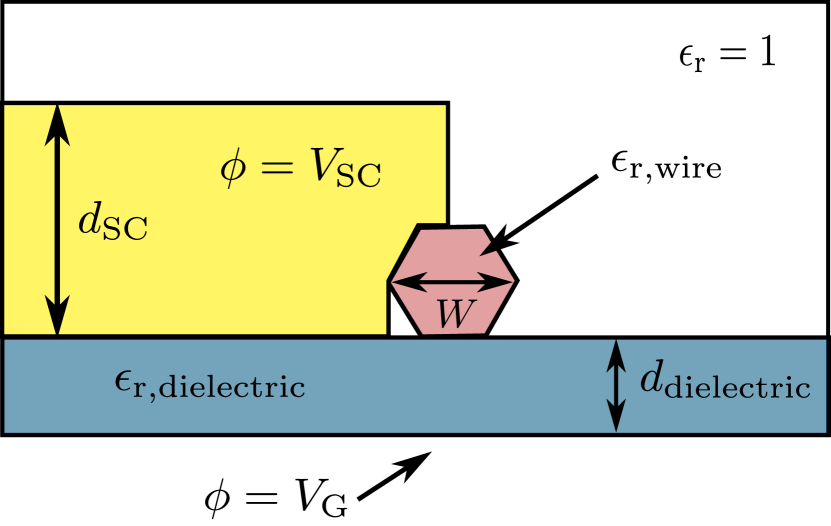
We discuss electrostatic effects in a device design as used by Mourik et al Mourik et al. (2012), however our methods are straightforward to adapt to similar layouts (see App. B for a calculation using a different geometry). Since we are interested in the bulk properties, we require that the potential and the Hamiltonian terms are translationally invariant along the wire axis and we consider a 2D cross section, shown in Fig. 1. The device consists of a nanowire with a hexagonal cross section of diameter on a dielectric layer with thickness . A superconductor with thickness covers half of the wire. The nanowire has a dielectric constant (InSb), the dielectric layer has a dielectric constant (Si3N4). The device has two electrostatic boundary conditions: a fixed gate potential set by the gate electrode along the the lower edge of the dielectric layer and a fixed potential in the superconductor, which we model as a grounded metallic gate. We set this potential to either , disregarding a work function difference between the NbTiN superconductor and the nanowire, or we assume a small work function difference Haneman (1959); Wilson (1966) resulting in .
We model the electrostatics of this setup using the Schrödinger-Poisson equation. We split the Hamiltonian into transverse and longitudinal parts. The transverse Hamiltonian reads
| (1) |
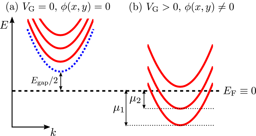
with the transverse directions, the effective electron mass in InSb (with the electron mass), the electron charge, and the electrostatic potential. We assume that in the absence of electric field the Fermi level in the nanowire is in the middle of the semiconducting gap , with for InSb (see Fig. 2(a). We choose the Fermi level as the reference energy such that .
The longitudinal Hamiltonian reads
| (2) |
with the direction along the wire axis, the spin-orbit coupling strength, the Zeeman energy and the Pauli matrices. The orientation of the magnetic field is along the wire in the direction. In this separation, we have assumed that the spin-orbit length is larger or comparable to the wire diameter, . Scheid et al. (2009); Diez et al. (2012) Furthermore, we neglect the explicit dependence of the spin-orbit strength on the electric field. We ignore orbital effects of the magnetic field, Nijholt and Akhmerov (2015) since the effective area of the transverse wave functions is much smaller than the wire cross section due to screening by the superconductor, as we show in Sec. III.
Since the Hamiltonian is separable in the limit we are using, the charge density in the transverse direction is:
| (3) |
with the transverse wave function and the subband energy of the -th electron mode defined by . Further, is the 1D electron density, which we calculate in closed form from the Fermi momenta of different bands in App. C. The subband energies depend on the electrostatic potential , and individual subbands are occupied by “lowering” subbands below (shown schematically in Fig. 2(b)). 111Note that agrees with the subband bottom only if and =0. See App. C for details on the subband occupation in the general case.
The Poisson equation that determines the electrostatic potential has the general form:
| (4) |
with the dielectric permittivity. Since the charge density of Eq. (3) depends on the eigenstates of Eq. (1), the Schrödinger and the Poisson equations have a nonlinear coupling.
We calculate the eigenstates and eigenenergies of the Hamiltonian of Eq. (1) in tight-binding approximation on a rectangular grid using the Kwant package Groth et al. (2014). We then discretize the geometry of Fig. 1 using a finite element mesh, and solve Eq. (4) numerically using the FEniCS package Logg et al. (2012).
Eqs. (1) and (3) together define a functional , yielding a charge density from a given electrostatic potential . Additionally, Eq. (4) defines a functional , giving the electrostatic potential produced by a charge density . The Schrödinger-Poisson equation is self-consistent when
| (5) |
We solve Eq. (5) using an iterative nonlinear Anderson mixing method Eyert (1996). We find that this method prevents the iteration process from oscillations and leads to a significant speedup in computation times compared to other nonlinear solver methods (see App. E). We search for the root of Eq. (5) rather than for the root of
| (6) |
since we found Eq. (5) to be better conditioned than Eq. (6). The scripts with the source code as well as resulting data are available online as ancillary files for this manuscript.
II.2 Majorana zero modes in superconducting nanowires
Having solved the electrostatic problem for the normal system, i.e. taking into account only the electrostatic effects of the superconductor, we then use the electrostatic potential in the superconducting problem. To this end, we obtain the Bogoliubov-de Gennes Hamiltonian by summing and and adding an induced superconducting pairing term:
| (7) |
with the Pauli matrices in electron-hole space and the superconducting gap.
The three-dimensional BdG equation (7) is still separable and reduces for every subband with transverse wave function to an effective one-dimensional BdG Hamiltonian:
| (8) |
where and we defined (see Fig. 2(b). Since the different subbands are independent, can be interpreted as the chemical potential determining the occupation of the -th subband.
While the Fermi level is kept constant by the metallic contacts, the chemical potential of each subband does depend on the system parameters: . Most of the model Hamiltonians for Majorana nanowires used in the literature are of the form of Eq. (8) (or a two-dimensional generalization) using one chemical potential . To make the connection to our work, should be identified with , and not be confused with the constant Fermi level . For example, the constant chemical potential limit of Ref. Das Sarma et al., 2012 refers to the special case that is independent of , and it is not related to being always constant. 222Using the notion of a variable chemical potential is natural when energies are measured with respect to a fixed band bottom, i.e. in a single-band situation. For us, different subbands react differently on changes in and it is more practical to keep the Fermi level fixed.
Properties of Majorana modes formed in the -th subband only depend on the value of (or equivalently ). In the following we thus determine the effect of the electrostatics on before we finally turn to Majorana bound states.
III Screening effects on charge density and energy levels
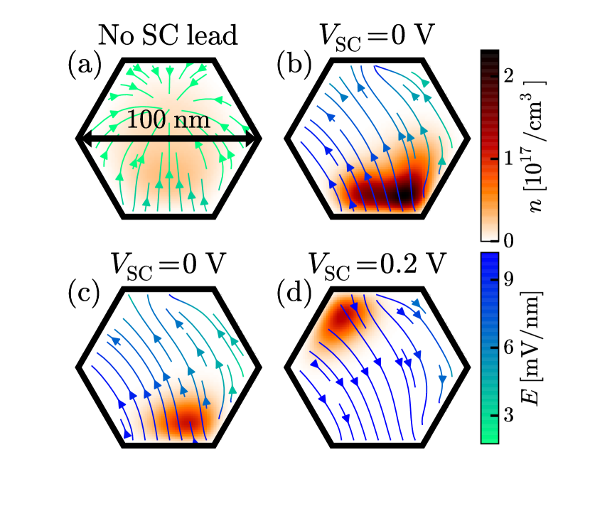
We begin by investigating the electrostatic effects in absence of Zeeman field and a spin-orbit strength with , negligible for the electrostatic effects. We solve the Schrödinger-Poisson equation for a superconductor with and a superconductor with , and compare the solutions to two benchmarks: a nanowire without a superconducting lead, and a nanowire in which we ignore screening by charge. Specifically, we compute the influence of screening by the superconductor and by charge on the field effect on the lowest energy levels and charge densities. To evaluate the role of screening by charges in the wire, we compare the full solutions of the Poisson equation (4) to its solution with the right-hand side set to zero. Our results are summarized in Fig. 3 showing the dispersion of and Fig. 4 showing the charge density for the same situations and the values of marked in Fig. 3.
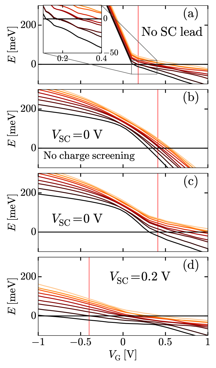
The approximate rotational symmetry of the wire leads to almost doubly degenerate bands with opposite angular momenta when electric field is negligible—a situation realized either in absence of the superconductor [Fig. 3(a)] or when [Fig. 3(b), (c), (d)]. However in most cases, presence of the superconductor leads to a large required to induce a finite charge density in the wire, and the degeneracy is strongly lifted.
The lever arm of the gate voltage on the energies , reduces from the optimal value of , at by approximately a factor of due to charge screening alone [Fig. 3(a)]. Screening by the superconductor leads to an additional comparable suppression of the lever arm, however its effect is nonlinear in due to the transverse wave functions being pulled closer to the gate at positive . Comparing panels (b) and (c) of Fig. 3 we see that screening by the superconductor does not lead to a strong suppression of screening by charge when : the field effect strongly reduces as soon as charge enters the wire when we take charge screening into account. This lack of interplay between the screening by superconductor and by charge can be understood by looking at the charge density distribution in the nanowire [Fig. 4(b), (c)]. Since a positive gate voltage is required to induce a finite charge density, the charges are pulled away from the superconductor, and the corresponding mirror charges in the superconductor area located at a distance comparable to twice the wire thickness. On the contrary, a positive requires a compensating negative to induce comparable charge density in the wire, pushing the charges closer to the superconductor [Fig. 4(d)]. In this case, the proximity of the electron density to the superconductor leads to the largest suppression of the lever arm, and proximity of image charges almost completely compensates the screening by charge.
The Van Hove singularity in the density of states leads to an observable kink in each time an extra band crosses the Fermi level [inset in Fig. 3(a)]. However, we observe that the effect is weak on the scale of level spacing and cannot guarantee strong pinning of the Fermi level to a band bottom.
IV Electrostatic response to the Zeeman field
IV.1 Limit of large level spacing
The full self-consistent solution of the Schrödinger-Poisson equation is computationally expensive and also hard to interpret due to a high dimensionality of the space of unknown variables. We find a simpler form of the solution at a finite Zeeman field relying on the large level spacing in typical nanowires. It ensures that the transverse wave functions stay approximately constant, i.e. up to magnetic fields of . In this limit we may apply perturbation theory to compute corrections to the chemical potential for varying .
We write the potential distribution for a given in the form
| (9) |
where is the potential obeying the boundary conditions set by the gate and the superconducting lead, and solves the Laplace equation
| (10) |
The corrections to this potential due to the charge contributed by the -th mode out of the modes below the Fermi level then obeys a Poisson equation with Dirichlet boundary conditions (zero voltage on the gates):
| (11) |
where we write the chemical potential at a finite value of as where is the chemical potential in the absence of a field.
We now define a magnetic field-independent reciprocal capacitance as
| (12) |
which solves the Poisson equation
| (13) |
Having solved the Schrödinger-Poisson problem numerically for , we define and . The correction to the subband energy is then given in first order perturbation as
| (14) |
Using Eqs. (12), (14) and we then arrive at:
| (15) |
with the elements of the reciprocal capacitance matrix given by
| (16) |
Solving the Eq. (15) self-consistently, we compute corrections to the initial chemical potentials . The Eq. (15) has a much lower dimensionality than Eq. (5) and is much cheaper to solve numerically. Further, all the electrostatic phenomena enter Eq. (15) only through the reciprocal capacitance matrix Eq. (16).
IV.2 Single- and multiband response to the magnetic field
We start by computing the electrostatic response to changes in the magnetic field when the Fermi level is close to the band bottom for a single band (, and we write the index for brevity). We study the influence of the electrostatic environment and assess whether the device is closer to a constant charge density or constant chemical potential situation (using the nomenclature of Ref. Das Sarma et al., 2012 explained in App. A).
The top panel of Fig. 5 shows the chemical potential response to Zeeman field. Without a superconducting contact, the electron-electron interactions in the nanowire are screened the least, and the Coulomb effects are the strongest, counteracting density changes in the wire. In agreement with this observation, we find the change in chemical potential comparable to the change in . Hence, in this case the system is close to a constant-density regime.
A superconducting contact close to the nanowire screens the electron-electron interaction in the wire due to image charges. The chemical potential is then less sensitive to changes in magnetic field. We find that this effect is most pronounced for a positive work function difference with the superconductor , when most of the electrons are pulled close to the superconducting contact. Then, the image charges are close to the electrons and strongly reduce the Coulomb interactions. In this case the system is close to a constant chemical potential regime. For screening from the superconducting contact is less effective, since electric charges are further away from the interface with the superconductor. Therefore in this case, we find a behavior intermediate between constant density and constant chemical potential.
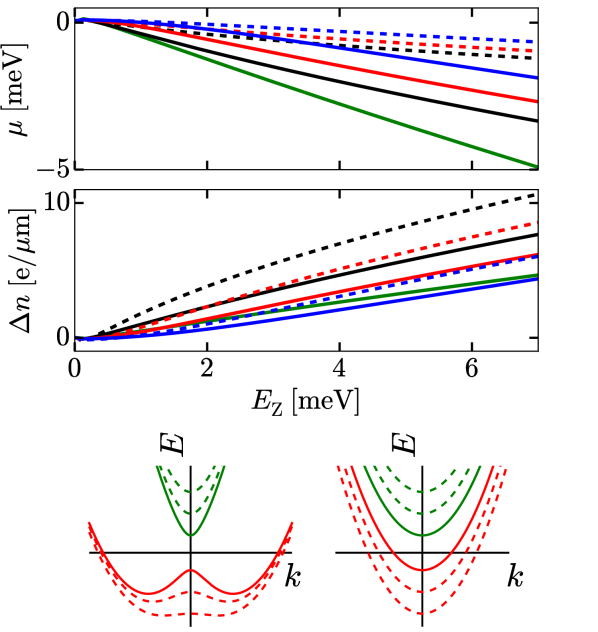
Besides the dependence on the electrostatic surrounding, the magnetic field response of the chemical potential depends on the spin-orbit strength. Specifically, the chemical potential stays constant over a longer field range when the spin-orbit interaction is stronger. 333Although we decrease the spin-orbit length to , which is smaller than the wire diameter of , we assume separable wave functions. Screening by the superconductor strongly localizes the wave functions, such that the confinement is still smaller than the spin-orbit length. The bottom panel of Fig. 5 explains this: when the spin-orbit energy , the lower band has a W-shape (bottom left). A magnetic-field increase initially transforms the lower band back from a W-shape to a parabolic band, as indicated by the dashed red lines. During this transition, the Fermi wavelength is almost constant. Since the electron density is proportional to the Fermi wavelength, this means that both the density and the chemical potential change very little in this regime. We thus identify the spin-orbit interaction as another phenomenon driving the system closer to the constant chemical potential regime, similar to the screening of the Coulomb interaction by the superconductor.
At large Zeeman energies , the spin-down band becomes parabolic (bottom right of Fig. 5). This results in the slope of becoming independent of the spin-orbit coupling strength, as seen in the top panel of Fig. 5 at large values of .
Close to the band bottom and when spin-orbit interaction is negligible, we study the asymptotic behavior of and by combining the appropriate density expression Eq. 28 with the corrections in the chemical potential Eq. 15. In that case, the chemical potential becomes
| (17) |
We associate an energy scale with the reciprocal capacitance , given by
| (18) |
and study the two limits and . In the strong screening limit we find the asymptotic behavior , corresponding to a constant-density regime. The opposite limit yields , close to a constant chemical potential regime. We computed explicitly for the chemical potential variations as shown in the top panel of Fig. 5. For a nanowire without a superconducting lead, we find an energy , indicating a constant-density regime. Using the classical approximation of a metallic cylinder above a metallic plate, we find an energy of the same order of magnitude. For a nanowire with an attached superconducting lead at , we get , intermediate between constant density and constant chemical potential. Finally, a superconducting lead at yields , indicating a system close to the constant chemical potential regime.
Since integrating over density-of-states measurements yields , the inverse self-capacitance can be inferred from experimental data by fitting the density variation curves to the theoretical dependence . This allows to experimentally measure the effect of the electrostatic environment, knowing the remaining Hamiltonian parameters.
We compare the response to Zeeman field in the multi-band case for and to the single band behavior in Fig. 6. We observe that presence of extra charges further reduces the sensitivity of the chemical potential to the magnetic field. We interpret the non-monotonous behavior of the chemical potential (most pronounced for in Fig. 6, but in principle present for all ) as being due to a combination of the Van Hove singularities in the density of states and screening by charges. For a fixed chemical potential, the upper band, moving up in energy due to the magnetic field, loses more states than the lower band acquires, since it approaches the Van Hove singularity in its density of states. To keep the overall density fixed, the chemical potential increases. Once the density in the lower band equals the initial density, the upper band is empty and the chemical potential starts dropping again. In the limit of constant density and a single mode the magnetic field dependence of the chemical potential can be solved analytically, reproducing the non-monotonicity and kinks (see App. D).
Relating the variation in to density measurements is experimentally inaccessible for , since corrections to depend on the density changes of each individual mode, as expressed in Eq. (15).
V Impact of electrostatics on Majorana properties
V.1 Shape of the Majorana phase boundary
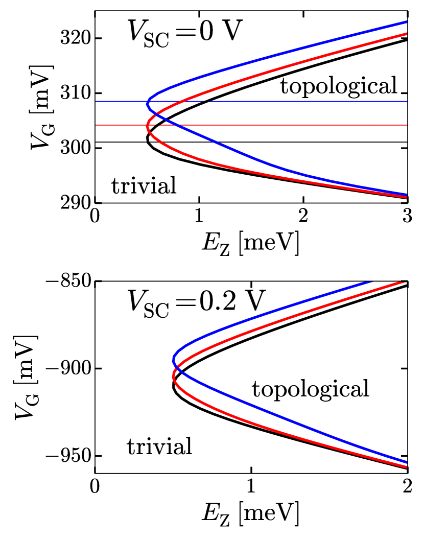
The nanowire enters the topological phase when the bulk energy gap closes at a Zeeman energy of . The electrostatic effects affect the shape of the topological phase boundary through the dependence of on . To find the topological phase boundary as a function of both experimentally controllable parameters and , we perform a full self-consistent simulation at . We then compute corrections to the resulting chemical potential at arbitrary using Eq. (15), and find topological phase boundary by recursive bisection.
Figure 7 shows the resulting phase boundary corresponding to . The phase boundary has a non-universal shape due to the interplay between electrostatics and magnetic field. In agreement with our previous conclusions, the electrostatic effects are the strongest with absent work function difference (top panel of Fig. 7) when the nanowire is intermediate between constant density and constant chemical potential. 444The presence of a superconductor is essential for Majorana fermions, but inevitably leads to screening. For the geometries of our calculations we thus do not have a situation close to constant density. Close to the band bottom, the charge screening reduces changes in density, and thus lowers the chemical potential by an amount that is similar to . Hence, the lower phase boundary (at smaller ) has a weaker slope than the upper phase boundary (at larger ). Note that in the limit of constant density, the lower phase boundary would be a constant independent of (see App. D).
For a work function difference , the system is closer to the constant chemical potential regime. In this regime, changes linearly with , yielding a hyperbolic phase boundary with symmetric upper and lower arms and its vertex at . When spin-orbit interaction is strong, a transition in the lower arm of the phase boundary from constant chemical potential (hyperbolic phase boundary) to constant density (more horizontal lower arm) occurs, resulting in a ‘wiggle’ which is most pronounced for and . This feature is less pronounced for due to the screening by the superconductor suppressing the Coulomb interactions.
V.2 Oscillations of Majorana coupling energy
The wave functions of the two Majorana modes at the endpoints of a finite-length nanowire have a finite overlap that results in a finite nonzero energy splitting of the lowest Hamiltonian eigenstates Cheng et al. (2009, 2010); Prada et al. (2012); Das Sarma et al. (2012); Rainis et al. (2013). This splitting oscillates as a function of the effective Fermi wave vector as Das Sarma et al. (2012). We investigate the dependency of the oscillation frequency, or the oscillation peak spacing on magnetic field and the electrostatic environment.
A peak in the Majorana splitting energy occurs when Majorana wave functions constructively interfere, or when the Fermi momentum equals , with the peak number and the nanowire length. The momentum difference between two peaks is
| (19) |
where is the Zeeman energy corresponding to the -th oscillation peak. In the limit of small peak spacing, we expand to first order in :
| (20) |
yielding the peak spacing
| (21) |
Since , we substitute
| (22) |
We obtain the values of and from the analytic expression for , presented in App. C. The value results from the dependence shown in Fig. 5.
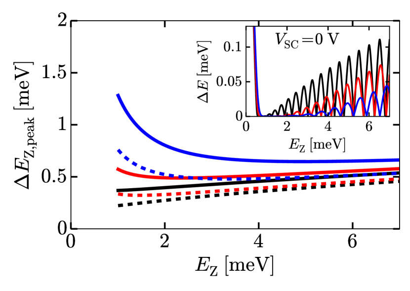
Fig. 8 shows the peak spacing as a function of for a nanowire of length . Stronger screening reduces the peak spacing (i.e. increases the oscillation frequency) by reducing the sensitivity of the chemical potential to the magnetic field, as discussed in Sec. IV. In addition, spin-orbit strength has a strong influence on the peak spacing, since for the density and thus stay constant. This results in a lower oscillation frequency and hence a larger peak spacing. Correspondingly, we find that the peak spacing may increase, decrease, or roughly stay constant as a function of the magnetic field.
Similarly to the shape of the Majorana transition boundary, Fig. 8 shows that the peak spacing does not follow a universal law, in contrast to earlier predictions Rainis et al. (2013). In particular, our findings may explain the zero-bias oscillations measured in Ref. Churchill et al., 2013, exhibiting a roughly constant peak spacing.
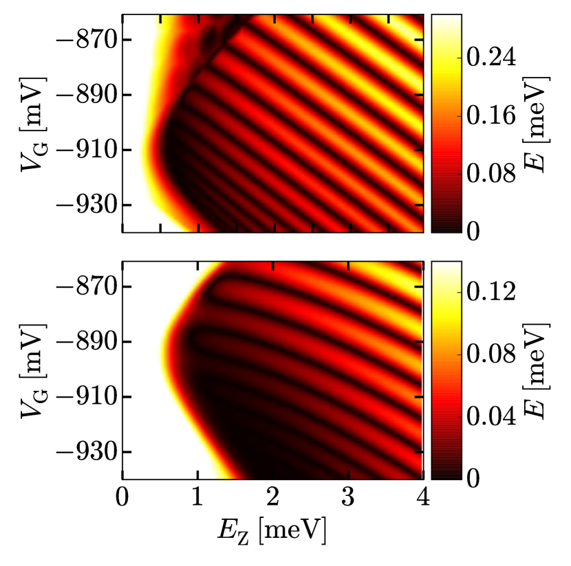
Fig. 9 shows Majorana energy oscillations as a function of both gate voltage and magnetic field strength for , with to increase the Majorana coupling. The diagonal ridges are lines of constant chemical potential. The difference in slope between the ridges of both plots indicates a difference in the equilibrium situation: closer to constant density for weak spin-orbit coupling, closer to constant chemical potential for strong spin-orbit coupling. The bending of the constant chemical potential lines in the lower panel indicates a transition from the latter mechanism to the former mechanism, due to the increase of magnetic field, as explained in Sec. IV.
VI Summary
We have studied the effects of the electrostatic environment on the field control of Majorana devices and their properties. Screening by charge and by the superconductor strongly reduce the field effect of the gates. Furthermore, screening by the superconductor localizes the charge and induces a large internal electric field. When we assume the superconductor to have a zero work function difference with the nanowire, charge localizes at the bottom of the wire, which reduces the induced superconducting gap.
Coulomb interaction causes the chemical potential to respond to an applied magnetic field, while screening by the superconductor and spin-orbit interaction suppress this effect. If a superconductor is attached, the equilibrium regime is no longer close to constant density, but either intermediate between constant density and constant chemical potential for a superconductor with zero work function difference, or close to constant chemical potential for a superconductor with a positive work function difference. An increasing spin-orbit interaction also reduces the response of the chemical potential.
Due to this transition in equilibrium regime for increasing screening and spin-orbit interaction, the shape of the Majorana phase boundary and the oscillations of Majorana splitting energy, depend on device parameters instead of following a universal law.
We have shown how to relate the measurement of density variations to the chemical potential response. Since the Majorana signatures directly depend on this response, our work offers a way to compare direct experimental observations of both signatures with theoretical predictions, and to remove the uncertainty caused by the electrostatic environment.
Our Schrödinger-Poison solver, available in the supplementary files for this manuscript, can be used to compute lever arms and capacities for different device dimensions and geometries, providing practical help for the design and control of experimental devices.
Acknowledgements.
We thank R. J. Skolasiński for reviewing the code, T. Hyart and P. Benedysiuk for valuable discussion. This research was supported by the Foundation for Fundamental Research on Matter (FOM), Microsoft Corporation Station Q, the Netherlands Organization for Scientific Research (NWO/OCW) as part of the Frontiers of Nanoscience program, and an ERC Starting Grant.Appendix A Nomenclature – constant density and constant chemical potential
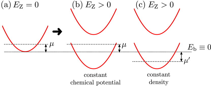
In Ref. Das Sarma et al., 2012 Das Sarma et al. considered Majorana oscillations as a function of magnetic field. The authors considered there two extreme electrostatic situations that they refer to as constant chemical potential and constant density.
In particular, Ref. Das Sarma et al., 2012 considers a one-dimensional nanowire BdG Hamiltonian as in Eq. (8), with being denoted as . In this model, the subband energy is fixed and set to . The electron density is changed by adjusting (shown for the case in Fig. 10(a).
For fixed in Eq. (8) electron density will change upon changing . For example, if , electron density will increase monotonically as is increased (see Fig. 10(b). This constant chemical potential situation is realized in the limit of vanishing Coulomb interaction, as then density changes do not influence the electrostatic potential. The same assumption is used in Refs. Prada et al., 2012; Rainis et al., 2013.
Appendix B Lever arms in an InAs-Al nanowire
Another promising set of devices for the creation of Majorana zero modes is an epitaxial InAs-Al semiconductor–superconductor nanowire. These systems exhibit a hard superconducting gap and a high interface quality due to the epitaxial growth of the Al superconductor shell Chang et al. (2015).
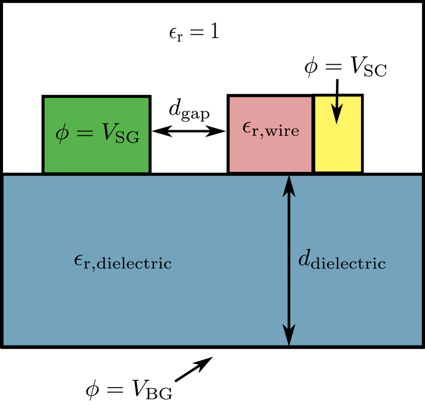
Figure 11 shows a cross section of the device. The nanowire (InAs) lies on an dielectric layer (SiO2) of thickness and is connected on one side to an Al superconducting shell. The device has two gates: a global back-gate with a gate potential , and a side gate with a potential , separated by a vacuum gap of width . We model the superconductor again as a metal with a fixed potential . These three potentials form the boundary conditions of the system.
We estimate the dependence of the lever arm of the side date on using the self-consistent Schrödinger-Poisson simulations. We set the back gate to , and choose the work function difference of the Al shell equal to , such that one electron mode is present at a side gate voltage of , with , as was observed in experiments Deng (2015). We use the band gap for InAs.
Our results are shown in Fig. 12, and allow to translate the gate voltages into the nanowire chemical potential. The work for the InAs-Al device shows that our numerical algorithm is easily adjusted to different device geometries, as long as the nanowire stays translationally invariant.
Appendix C Electron density in a nanowire
Integration over the 1D density of states yields the electron density , related to the charge density by Eq. (3). To derive the density of states, we start from the nanowire Hamiltonian, consisting of the transverse Hamiltonian of Eq. (1) and the longitudinal Hamiltonian of Eq. (2):
| (23) |
Assuming that the wave function has the form of a plane wave in the longitudinal direction, and quantized transverse modes with corresponding energies in the transverse direction (where denotes the transverse mode number), the energies of the Hamiltonian are
| (24) |
yielding the dispersions of the upper and the lower spin band. Converting Eq. (24) to momentum as a function of energy yields
| (25) |
where , , , and are in units of . The relation between the density of states and is
| (26) |
We obtain the density by integrating the density of states up to the Fermi level . The Zeeman field opens a gap of size between the upper and the lower spin band. Due to the W-shape of the lower spin band, induced by the spin-orbit interaction, we distinguish three energy regions in integrating up to . If , both spin bands are occupied and the integration yields
| (27) |
If , only the lower band is occupied, and the dispersion has two crossings with the Fermi level, yielding a density
| (28) |
For a nonzero spin-orbit strength, we have four crossings of the lower spin band with if (see Fig. 5, bottom panel). Since only the interval contributes to the density, integration of the density of states yields
| (29) |
Appendix D Response to the Zeeman field in the constant density limit and for small spin-orbit
The limit of small spin-orbit interaction and constant electron density in the nanowire independent of Zeeman field allows for an analytic solution the magnetic field dependence of the chemical potential, . In particular, we have from Eqs. (27) and (29) for :
| (30) |
where is the Heaviside step function. This is readily solved as
| (31) |
Hence, the chemical potential first increases with increasing until the upper spin-band is completely depopulated. Then the chemical potential decreases linearly with . At the cross-over point the dependence of the chemical potential is not smooth but exhibits a kink, also seen for example in the numerical results of Fig. 6.
In the constant density limit we can also compute the asymptotes of the topological phase in --space. For , the topological phase coincides with the chemical potential range where only one spin subband is occupied. From Eq. (31) we find the two asymptotes thus as and . Hence, in the constant density limit, the phase boundary that corresponds to depleting the wire becomes magnetic field independent.
Appendix E Benchmark of nonlinear optimization methods
We apply the Anderson mixing scheme to solve the coupled nonlinear Schrödinger-Poisson equation:
| (32) |
Optimization methods find the root of the functional form of Eq. (32), as given in Eq. (5). As opposed to other methods, the Anderson method uses the output of last rounds as an input to the next iteration step instead of only the output of the last round. Eyert (1996) The memory of the Anderson method prevents the iteration scheme from oscillations and causes a significant speedup in computation times in comparison to other methods, and in particular the simple under-relaxation method often used in nanowire simulations.Wang et al. (2006); Chin et al. (2009)
As a test system, we take a global back gate device, consisting of a hexagonal InSb nanowire on an dielectric layer (SiO2) of thickness , without a superconducting lead. Due to the thick dielectric layer in comparison to the Majorana device, this device is more sensitive for charge oscillations (a different number of electron modes in the system between two adjacent iteration steps). This makes the device well-suited for a performance benchmark. We compare the Anderson method to three other nonlinear optimization methods: Broyden’s First and Second method Broyden (1965) and a method implementing a Newton-Krylov solver (BiCG-stab) Knoll and Keyes (2004).
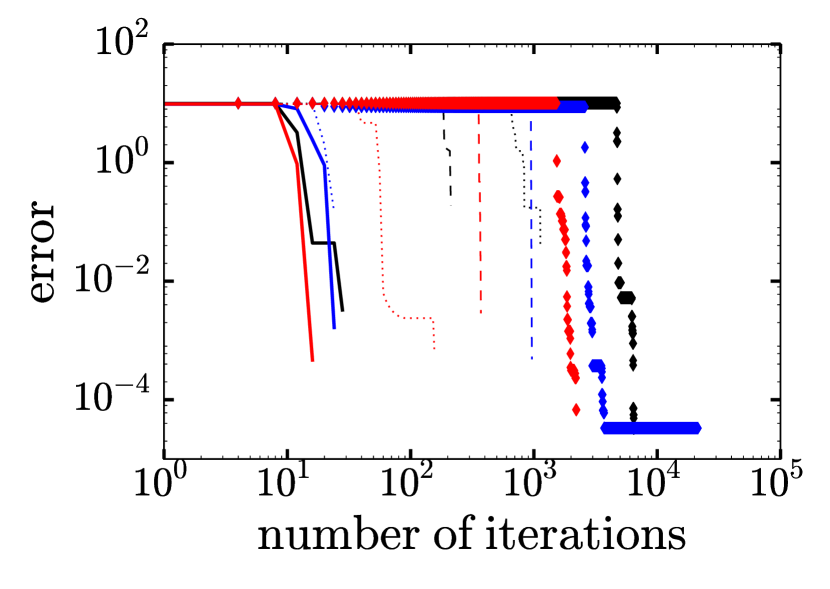
Fig. 13 shows the results. In this plot, we show the cumulative minimum of the error. Plateaus in the plot correspond to regions of error oscillations. The figure shows that the Anderson method generally converges quickly and is not affected by error oscillations. However, the three other methods show oscillatory behavior of the error over a large range of iterations. Both Broyden’s methods perform worse than the Anderson method, but generally converge within iterations. The Newton-Krylov method performs the worst, having a large region of oscillations up to iterations. Due to its robustness against error oscillations, the Anderson method is the most suited optimization method for the Schrödinger-Poisson problem. For a much thinner dielectric layer, such as the 30 nm layer in the Majorana device, the iteration number is typically for all four tested optimization methods.
In our approach, we choose not to use a predictor-corrector approachTrellakis et al. (1997); Curatola and Iannaccone (2003) that can also be used together with a more advanced nonlinear solver such as the Anderson method.Wang et al. (2009) The advantage of the direct approach used here is its simplicity, without a significant compromise in stability and efficiency.
References
- Fu and Kane (2008) L. Fu and C. L. Kane, Phys. Rev. Lett. 100, 096407 (2008).
- Alicea (2012) J. Alicea, Rep. Prog. Phys. 75, 076501 (2012).
- Beenakker (2013) C. Beenakker, Annu. Rev. Con. Mat. Phys. 4, 113 (2013).
- Alicea et al. (2011) J. Alicea, Y. Oreg, G. Refael, F. von Oppen, and M. P. A. Fisher, Nat. Phys. (2011).
- Nayak et al. (2008) C. Nayak, S. H. Simon, A. Stern, M. Freedman, and S. Das Sarma, Rev. Mod. Phys. 80, 1083 (2008).
- Oreg et al. (2010) Y. Oreg, G. Refael, and F. von Oppen, Phys. Rev. Lett. 105, 177002 (2010).
- Lutchyn et al. (2010) R. M. Lutchyn, J. D. Sau, and S. Das Sarma, Phys. Rev. Lett. 105, 077001 (2010).
- Mourik et al. (2012) V. Mourik, K. Zuo, S. M. Frolov, S. R. Plissard, E. P. A. M. Bakkers, and L. P. Kouwenhoven, Science 336, 1003 (2012).
- Das et al. (2012) A. Das, Y. Ronen, Y. Most, Y. Oreg, M. Heiblum, and H. Shtrikman, Nat. Phys. 8, 887 (2012).
- Deng et al. (2012) M. T. Deng, C. L. Yu, G. Y. Huang, M. Larsson, P. Caroff, and H. Q. Xu, Nano Lett. 12, 6414 (2012).
- Churchill et al. (2013) H. O. H. Churchill, V. Fatemi, K. Grove-Rasmussen, M. T. Deng, P. Caroff, H. Q. Xu, and C. M. Marcus, Phys. Rev. B 87, 241401 (2013).
- Deng et al. (2014) M. Deng, C. Yu, G. Huang, M. Larsson, P. Caroff, and H. Xu, Sci. Rep. 4, 7621 (2014).
- Bagrets and Altland (2012) D. Bagrets and A. Altland, Phys. Rev. Lett. 109, 227005 (2012).
- Pikulin et al. (2012) D. I. Pikulin, J. P. Dahlhaus, M. Wimmer, H. Schomerus, and C. W. J. Beenakker, New J. Phys. 14, 125011 (2012).
- Stanescu et al. (2012) T. Stanescu, S. Tewari, J. Sau, and S. Das Sarma, Phys. Rev. Lett. 109, 266402 (2012).
- Fregoso et al. (2013) B. Fregoso, A. Lobos, and S. Das Sarma, Phys. Rev. B 88, 180507(R) (2013).
- Cheng et al. (2009) M. Cheng, R. Lutchyn, V. Galitski, and S. Das Sarma, Phys. Rev. Lett. 103, 107001 (2009).
- Cheng et al. (2010) M. Cheng, R. Lutchyn, V. Galitski, and S. Das Sarma, Phys. Rev. B 82, 094504 (2010).
- Prada et al. (2012) E. Prada, P. San-Jose, and R. Aguado, Phys. Rev. B 86, 180503 (2012).
- Das Sarma et al. (2012) S. Das Sarma, J. D. Sau, and T. D. Stanescu, Phys. Rev. B 86, 220506 (2012).
- Rainis et al. (2013) D. Rainis, L. Trifunovic, J. Klinovaja, and D. Loss, Phys. Rev. B 87, 024515 (2013).
- Haneman (1959) D. Haneman, J. Phys. Chem. Solids 11, 205 (1959).
- Wilson (1966) R. G. Wilson, J. Appl. Phys. 37, 3170 (1966).
- Scheid et al. (2009) M. Scheid, İnanç Adagideli, J. Nitta, and K. Richter, Semicond. Sci. Tech. 24, 064005 (2009).
- Diez et al. (2012) M. Diez, J. P. Dahlhaus, M. Wimmer, and C. W. J. Beenakker, Phys. Rev. B 86, 094501 (2012).
- Nijholt and Akhmerov (2015) B. Nijholt and A. R. Akhmerov, (2015), arXiv:1509.02675 [cond-mat.mes-hall] .
- Note (1) Note that agrees with the subband bottom only if and =0. See App. C for details on the subband occupation in the general case.
- Groth et al. (2014) C. Groth, M. Wimmer, A. Akhmerov, and X. Waintal, New J. Phys. 16, 063065 (2014).
- Logg et al. (2012) A. Logg, K. Mardal, and G. Wells, Automated Solution of Differential Equations by the Finite Element Method (Springer, 2012).
- Eyert (1996) V. Eyert, J. Comp. Phys. 124, 271 (1996).
- Note (2) Using the notion of a variable chemical potential is natural when energies are measured with respect to a fixed band bottom, i.e. in a single-band situation. For us, different subbands react differently on changes in and it is more practical to keep the Fermi level fixed.
- Note (3) Although we decrease the spin-orbit length to , which is smaller than the wire diameter of , we assume separable wave functions. Screening by the superconductor strongly localizes the wave functions, such that the confinement is still smaller than the spin-orbit length.
- Note (4) The presence of a superconductor is essential for Majorana fermions, but inevitably leads to screening. For the geometries of our calculations we thus do not have a situation close to constant density.
- Chang et al. (2015) W. Chang, S. Albrecht, T. Jespersen, F. Kuemmeth, P. Krogstrup, J. Nygård, and C. Marcus, Nat. Nanotechnol. 10, 232 (2015).
- Deng (2015) M. Deng, private communication (2015).
- Wang et al. (2006) L. Wang, D. Wang, and P. M. Asbeck, Solid-State Electron. 50, 1732 (2006).
- Chin et al. (2009) S. Chin, V. Ligatchev, S. Rustagi, H. Zhao, G. Samudra, N. Singh, G. Lo, and D.-L. Kwong, IEEE Trans. Electron Dev. 56, 2312 (2009).
- Broyden (1965) C. Broyden, Math. Comp. 19, 577 (1965).
- Knoll and Keyes (2004) D. Knoll and D. Keyes, J. Comp. Phys. 193, 357 (2004).
- Trellakis et al. (1997) A. Trellakis, A. Galick, A. Pacelli, and U. Ravaioli, J. Appl. Phys. 81, 7880 (1997), cited By 177.
- Curatola and Iannaccone (2003) G. Curatola and G. Iannaccone, Comput. Mater. Sci. 28, 342 (2003).
- Wang et al. (2009) H. Wang, G. Wang, S. Chang, and Q. Huang, Micro Nano Lett. 4, 122 (2009).