Charge Trap Memory Based on Few-Layered Black Phosphorus
Atomically thin layered two-dimensional materials, including transition-metal dichacolgenide (TMDC) and black phosphorus (BP), (?) have been receiving much attention, because of their promising physical properties and potential applications in flexible and transparent electronic devices . Here, for the first time we show non-volatile charge-trap memory devices, based on field-effect transistors with large hysteresis, consisting of a few-layer black phosphorus channel and a three dimensional (3D) Al2O3 /HfO2 /Al2O3 charge-trap gate stack. An unprecedented memory window exceeding 12 V is observed, due to the extraordinary trapping ability of HfO2. The device shows a high endurance and a stable retention of 25 charge loss after 10 years, even drastically lower than reported MoS2 flash memory. The high program/erase current ratio, large memory window, stable retention and high on/off current ratio, provide a promising route towards the flexible and transparent memory devices utilising atomically thin two-dimensional materials. The combination of 2D materials with traditional high- charge-trap gate stacks opens up an exciting field of nonvolatile memory devices.
Introduction
Nonvolatile memory cells, which are essential components for digital, portable and self-standing electronics, attract more and more attention, since the miniaturization, low power consumption and reliable data storage are highly desirable to solve the problem of large data capacity, integration density. Memories based on ultrathin layered two-dimensional (2D) materials like graphene and transition-metal dichalcogenides (TMDCs), such as MoS2, even graphene-oxide which can act as field effect transistor (FET) channel, charge-trapping layer or electrode, have been demonstrated and considered to be promising candidates, due to their fantastic electronic properties and potential applications (?, ?, ?, ?, ?, ?, ?, ?). It was shown that the large hysteresis in the gate characterization curves of FETs can be applied for memory devices operation. Despite the extremely high mobility in graphene, the absence of a band gap hinders the achievement of a high ON/OFF ratio (?, ?). This has led to intensive research in other 2D materials that have an intrinsic band gap. Among them, TMDCs, such as MoS2 and WS2, which have finite band gaps, not only have enabled the fabrication of high-performance field-effect transistor (FET) devices but have also paved the way for the realization of novel optoelectronic and valleytronic devices (?, ?, ?, ?, ?, ?). Recently, black phosphorus monolayer, as well as its multilayers have been extensively studied (?, ?, ?, ?, ?, ?, ?, ?, ?). Comparing with TMDCs which have relatively low mobility, black phosphorus (BP) becomes an outstanding new element 2D layered material, with high mobility value of 1000 cm2V-1s-1 and 3900 cm2V-1s-1 at room temperature and low temperature, respectively (?, ?). BP is a van der waals type semiconducting layered material with a direct band gap of 0.3eV (bulk) to 2eV (monolayer), depending on the number of layers (?). The superior ambipolar property, higher mobility than TMDCs, comparable drain current modulation up to 105 with TMDCs, promise black phosphorus as a good candidate for memory devices (?, ?, ?, ?, ?). Moreover, nonvolatile memory based on black phosphorus also hold great promise for future flexible and transparent devices because of the mechanical flexible and tunable electronic properties of black phosphorus (?, ?, ?).
The selection of charge trapping layer and dielectrics is also significant because the applications of nonvolatile memory are still constrained by low charge retention and high operating voltage. In recent years, different structures of the memory devices have been investigated, by using graphene, MoS2 or high- oxide dielectric such as HfO2, HfAlO, HfON and TiO2 as the trapping layer (?, ?, ?, ?, ?, ?, ?). The related works indicate the high efficiency and potential application of HfO2 used as charge trapping layer (?, ?, ?, ?). Meanwhile, a high quality dense tunneling dielectric and high- blocking layer can provide low charge leakage and reduce the operating voltage as well as power consumption, respectively. Therefore, thanks to the high- HfO2 as the trapping layer while the Al2O3 of different thickness as the tunneling and blocking layer, the structure of Al2O3/HfO2/Al2O3 (AHA) gate stack can be utilised effectively in nonvolatile memory to obtain devices with excellent properties, such as good trap ability, low power consumption and outstanding thermal stability (?, ?, ?). However, to our knowledge, there is no black phosphorus involved nonvolatile memory device being reported yet. We expect to enhance the performance of memory devices by combining the few-layer black phosphorus with conventional Al2O3/HfO2/Al2O3 gate stack.
In this paper, we demonstrate memory devices fabricated from black phosphorus and high- HfO2. As expected, the device shows a significant hysteresis and a substantial memory window thanks to the superior trap capacity of the Al2O3/HfO2/Al2O3 (AHA) gate stack. Meanwhile, a robust charge retention of 70% retain after 10 years and stable endurance of more than 1200s and 120 cycles are obtained. The application of the conventional Al2O3/HfO2/Al2O3 gate stack renders a possibility for a massive production of high-performance of black phosphorus-based 2D memory devices.
Results and discussion
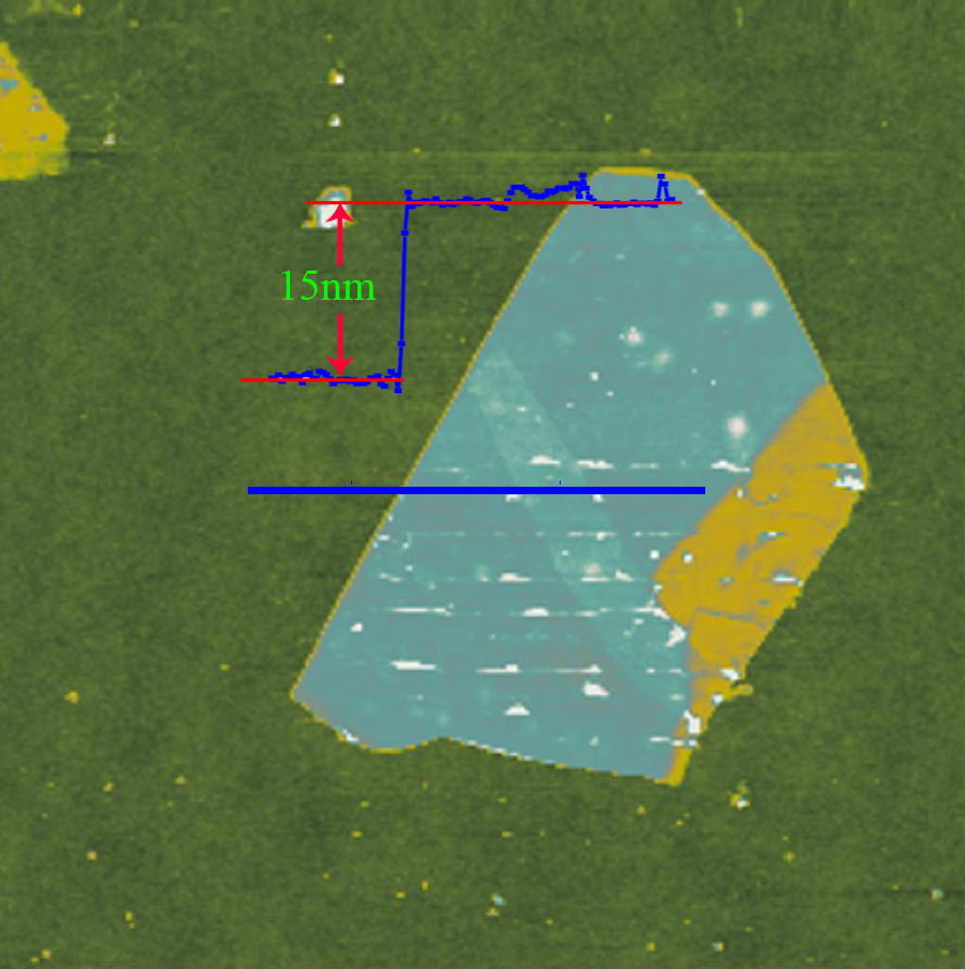
Few-layer black phosphorus is obtained through mechanical exfoliation from black phosphorus bulk crystals onto prepatterned SiO2/Si++ substrates with the thickness of SiO2 of 300 nm (?). We chose the particular flake with a thickness of 15 nm, as confirmed by atomic force microscopy, as extremely thin flakes ( 5 nm) have a low mobility of 10 cm2V-1s-1 (?, ?). Source and drain contacts of 5 nm/85 nm Ti/Au were deposited thermal evaporation. Subsequently, the Al2O3/HfO2/Al2O3 (AHA) gate stack was grown an atomic layer deposition (ALD) system with layer thickness of 5/8/35 nm, respectively. More details of device fabrication process can be found in the Methods.
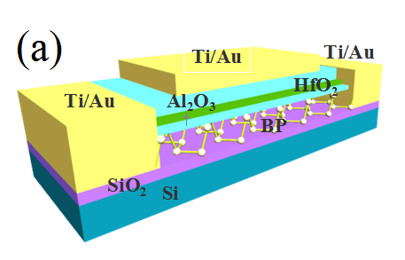

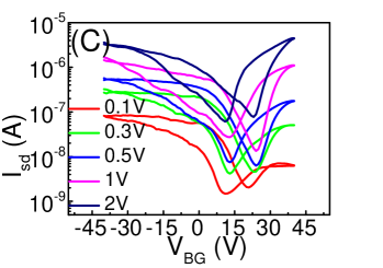
A typical device schematic is shown in Fig.1(a). The non-Ohmic contact was indicated in Fig.1(b) and sublinear dependence of Isd was clear in the small range as shown in the inset. An applied top-gate voltage (VTG) modulates the amount of charge stored in the HfO2 charge-trap layer, causing the variation of the conductivity of the BP channel. A back-gate voltage (VBG) was applied to the degenerately doped silicon substrate to tune the memory characteristics by systematically shifting the Fermi level of black phosphorus. We noted that through the ALD deposition process the device performance can be significantly improved because of the thermal annealing under vacuum (?, ?). Also, the encapsulation of black phosphorus in a high- dielectric environment will reduce the Coulomb scattering and modify the phonon dispersion in few-layer black phosphorus. Moreover, the oxide capping would protect the BP from ambient degradation (?, ?). The black phosphorus in our device is measured to be about 15 layers by atomic force microscopy. The transfer curve (IDS-VTG) of the device can be obtained by sweeping VTG while keeping the back gate grounded. When VBG is swept between -40 to +40 V, the appearance of the hysteresis between the forward and backward sweep curves indicates the interface effect from SiO2 and the black phosphorus channel, as shown in Fig.1(c).
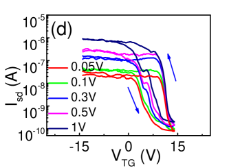
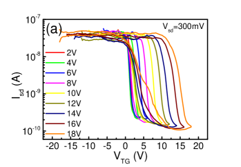
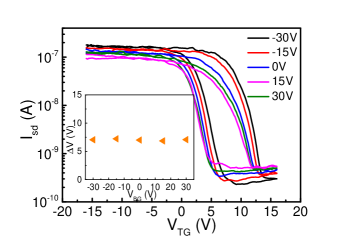
The transfer characteristics were explored to probe the storage capability of the black phosphorus memory device. As shown in Figure 1(d), with VBG = 0 V and different Vsd between 50mV and 1V, the transfer characteristic curves were obtained by sweeping VTG from -15V to +15V, then back to -15V, and a maximal on/off ratio about 104 was acquired. A large memory window of about 12 V was observed, primarily originated from a large amount of electrons and holes stored in the charge-trap layer of HfO2. The mobility degradation is likely due to the thickness of 15 nm of BP. When different voltage sweep rates are applied, negligible appreciable differences are noted in transfer curves. It indicates that the hysteresis of the transfer curve is not caused by the captured molecules, such as a thin layer of water, at the interface of BP/Al2O3 (?). The observed large gate hysteresis can be utilized for a nonvolatile memory device operation employing the BP layer as the channel.
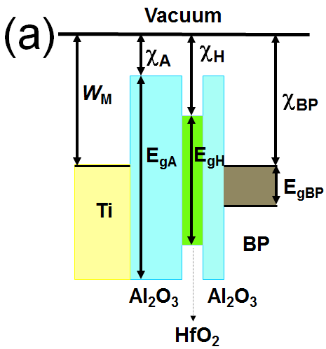
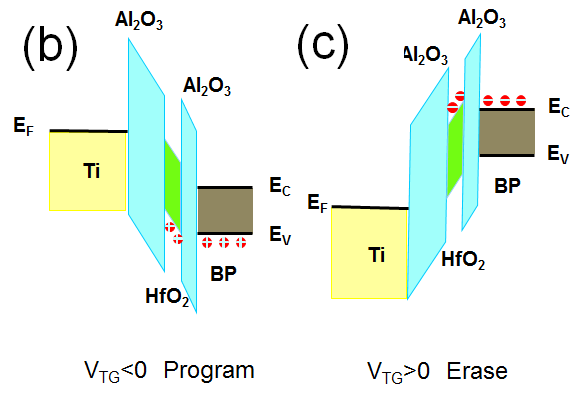
The band diagram of the BP CTM with the AHA stack is shown in Figure 2. The electron affinity of Al2O3 and HfO2 are 1eV and 2.5 eV, and the band gap are 7.7 eV and 4.9 eV, respectively (as shown in Fig.2(a)). The electron affinity of BP is about 4.4 eV and the band gap of bulk and monolayer BP are 0.3 eV and about 1.0 eV, respectively. In this situation, electron and hole potential well will be formed in the AHA stack layers structure, which can trap electrons and holes. In consideration of the 5 nm thick Al2O3, electrons can tunnel through the Al2O3 barrier by means of the mechanism of Fowler-Nordeim tunneling (?). In the device, the 5nm Al2O3-layer acts as tunnel layer, while 8nm HfO2-layer acts as trap layer.
As presented in Fig.2(b,c), negative and positive gate voltage applied to the top gate correspond to the program and erase states in the device operation process, respectively. In the program process, the shape of the energy band changes as shown in Fig.2 and the barrier of the tunneling oxide layer which is close to the BP film becomes thin enough for tunneling; hence, holes in BP layer can be pulled and transferred to HfO2-layer through the Al2O3 tunnel layer as a result of the Fowler-Nordeim tunneling effect (see Fig.2). The resultant accumulation of holes in HfO2 will shift the threshold voltage (Vth) to the negative direction, since this accumulation of holes in the HfO2 layer would screen the top-gate electric field effect. When the gate voltage is swept toward a higher positive value, the holes in trap layer will be pushed back to the BP channel; meanwhile, the electrons in conduction band of BP will be pulled into the trap layer which also can screen the top-gate electric field and cause the threshold voltage shifted to the positive direction (see Fig.2). Then, an appreciable memory window can be obtained in the transfer characteristic curve as a result of the capability of electron and hole trapping from AHA stack. As the top-gate voltage changes from positive to negative, the memory cell works in the program state, while as the top-gate voltage changes from negative to positive, the memory cell works in the erase state.
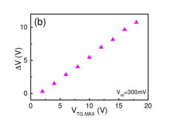
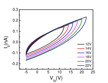
The amount of charge stored in the charge-trap layer can be modulated by gradually changing the maximum (+VTG.MAX) and minimum (-VTG.MIN) voltage applied on the top gate. Figure 3(a) shows the enlarged hysteresis window when becomes larger. The shift of the threshold voltage toward negative and positive direction corresponds to the hole and the electron trapping, respectively. The increased threshold voltage shift () as a function of VTG.MAX is summarized in Figure 3(b). The amount of charge stored in the charge-trap layer can be estimated from the expression:
| (1) |
where is the electron charge, is the threshold voltage shift toward the negative or the positive direction compare to the original transfer curve (?). According to Figure 3(a), the hysteresis window of the sweep between -2 and +2 V is close to zero, thus it can be defined as the original transfer curve, corresponding to no tunneled electrons or holes existing in the charge-trap layer. is the capacitance between the HfO2 charge-trap layer and the top gate, where is the vacuum permittivity, and are the relative dielectric constant ( 8) and thickness (35 nm) of the Al2O3 blocking layer, respectively.
Here, we define V =Vh + Ve , where Vh and Ve are the threshold voltage shift toward the negative and positive direction compare to the original transfer curve, corresponding to the density of stored holes and electrons, respectively. The calculated density of stored electrons and holes under —VTG.MAX— of 18V is on the order of 1014 and 1013 cm-2, respectively, which is in agreement with previously reported memory devices using graphene or graphene oxide as charge-trap layers (?, ?, ?). The lower tunneling barrier height of electrons than holes is accounted for the high trap density of electrons.
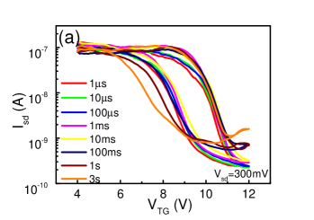

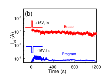
To study the dynamic transition rate of the black phosphorus memory device, a positive pulse (+16 V, duration of 3s) was applied to the top gate () to set the device in the erase state, followed by a -16 V pulse with different duration time. The reading procedure was performed by sweeping IDS-VTG in a very small range (+4 to +12 V) to minimize the effect of the measurements to the device’s state. After each reading operation, a positive pulse (+16 V, duration of 3s) was applied on the top gate to reset the device in the erase state. The threshold voltage shift VTH was acquired by applying in a linear fit to the linear regime of the reading IDS-VTG curve. Figure 4(a) shows a clear shift of the threshold voltage when the width of the pulse is changed to 10 ms, which sets a reference for the following dynamic behaviour measurements. VTH shows nearly a saturation behaviour when the pulse width increases to 3 s (Figure 4(a)). The charge-trapping rate can be estimated from the expression:
| (2) |
where VTH is the threshold voltage shift and t is the pulse width (?). The calculated charge-trapping rate varies from 1019 to 1012 cm-2t-1 when the pulse width changes from 1 s to 3 s. The reason for such a high charge-trap rate is because of the thin Al2O3 tunnel layer (only 5 nm), which makes electron/hole charges much easier to tunnel through.
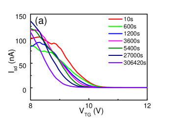
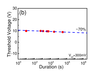
The retention characteristics of the device are determined by the height of the tunneling barrier and the depth of potential well formed in the Al2O3/HfO2/Al2O3 charge-trap stack (?, ?). Figure 5(a) shows the threshold voltage at different time intervals after programming the device with a negative pulse (-16 V, duration of 1s). The transfer curve was also obtained in a small voltage range (+4 to +12 V). The extracted threshold voltage VRTH varies from 4.5 to 3.4 V after 106 s(Figure 5(b)), from which we estimate that only 30 of the charges will be lost after 10 years. The enhancement of the retention characteristics of our black phosphorus memory device is also related to the extraordinary trapping ability of the Al2O3/HfO2/Al2O3 gate stack.
| Our work | 2D Memory | 2D memory | 2D memory | Organic memory | Organic memory | |
|---|---|---|---|---|---|---|
| MoS2 | Graphene | Graphene | ||||
| Channel material | Black phosphorus | MoS2 | Graphene | Graphene | pentacene | P3HT |
| Charge trapping layer | HfO2 | Graphene | MoS2 | GO | Au nano-crystal | Cu NPs |
| (few-layer) | (few-layer) | monolayer | ||||
| Barrier | Al2O3 | Al2O3/HfO2 | h-BN | Poly-vinylphenol | Al2O3 | PS or PVN |
| Memory window | 12V from 18V | 8Vfrom15V | 17Vfrom40V | 11.7Vfrom20V | 2.25Vfrom5V | 42.6Vfrom50V |
| Endurance | ¿120 | 120 | ¿100 | 200 | 1000 | ¿100 |
| Retention (/10 years) | 30%loss | 70%loss | 70%loss | —- | 40%loss per day | 80%loss |
| Operating power | Vsd=300mV | Vsd=50mV | Vsd=100mV | Vsd=1.5V | Vsd=3V | Vsd=20V |
| Pulse¡16V | Pulse¡18V | Pulse¡40V | Pulse¡20V | Pulse¡5V | Pulse¡50V | |
| Sample size | ||||||
| Lateral size | ¡5 m | ¡5 m | ¡5 m | 1mm | inches | |
| Thickness | 15nm | 1nm | ¡10nm | 1nm | 30nm |
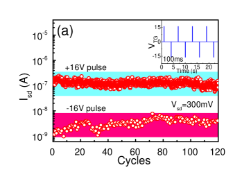
The retention of trapped charge data was then studied. Two states with different currents can be defined as ‘trap’ and ‘release’ states, corresponding to program state and erase state, respectively. The retention performance curve could show that if the trapped charge can be maintained without loss of charge. In addition, as shown in Fig.6(b), high Irelease/Itrap ratio of 102 can be obtained, comparing with memory device with floating gate utilising 2D materials, e.g. GBM. Most of devices measured in this work exhibit similar retention characteristics regardless of thickness of charge-trap layer and tunnelling barrier.
To test the endurance of the memory device, a sequence of pulse ( 16 V, duration of 100 ms) was applied to the top gate with V while IDS was measured (V mV). As presented in Figure 6(a), the charge trapping can be preserved over 100 cycles. Most memory devices relying on charge trapping suffer from problems related to charge retention, such as loss of charge by back-tunnelling, injection of carriers of the opposite type or redistribution of charge in defects (?). The robustness and stability of the device shows a great perspective of applications in nonvolatile memory technology.
As 2D materials like graphene, MoS2, even graphene oxide have received much attention in view of their application for nonvolatile memory, organic memories also have been studied as leading contending devices for future memory devices (?, ?, ?, ?, ?). Here, we compared the performances of our devices based on black phosphorus to those of reported memory devices based on other 2D materials and organic materials (Table 1). Compared with graphene and MoS2 charge trapping memories, the memory devices fabricated in our study display better performance with stable retention of 70% retain after 10 years, while the memory window and endurance comparable to these devices. In addition, in terms of memory window, retention, miniaturization and low energy consumption, the device discussed in our work is obviously superior than those of organic memories. So it is reasonable to believe that nonvolatile memory devices based on black phosphorus hold great promise for future flexible and transparent memory devices.
Conclusion
In conclusion, we have demonstrated a memory device based on few-layer black phosphorus and Al2O3 /HfO2 /Al2O3 charge-trap stack. All the devices studied showed similar hysteresis characteristics, regardless of the channel length and BP film thickness. From the measurement of retention and endurance characteristics, it was confirmed that high- dielectric HfO2 layer acts as an effective charge-trapping layer in this configuration. High on/off current ratio of 102, large memory window about 12 V at VTG=16V, long data retention that only 30% charge loss after 10 years, were attained. This study provides a promising route towrads the flexible and transparent memroy devices, utilising ultrathin two-dimensional materials.
Experimental section
Device fabrication
Thin layers of black phosphorus were mechanically exfoliated on a silicon wafer with 300 nm-thick SiO2. The flakes were identified by a combination of optical and scanning electron microscopy (JEOL). We used multilayer BP with a thickness of 15 nm and widths of around 5 m. The SiO2/Si++ is used as a back gate to control the carrier concentration in the BP. Source and drain electrodes of Ti (3 nm)/Au (85 nm) were fabricated on BP samples by standard electron-beam lithography (EBL), followed by thermal evaporation and metal lift-off techniques. Electrodes with width 0.3-0.8 m and a channel length of 0.5-2 m were used. The wafers was covered with polymethyl methacrylate (PMMA) e-beam resist immediately after exfoliation to avoid possible degradation upon longer exposure to air. After lift-off, stacked layers of Al2O3/HfO2/Al2O3 (5/8/35 nm) were deposited ALD. During the ALD process, trimethylaluminum and trtrakis (ethyl-methulamido) hafnium were reacted at 120 ∘C with water for Al2O3 and HfO2, respectively. The top-gate (Ti/Au 3 nm/50 nm) electrodes were subsequently fabricated using another EBL and metal deposition process.
Characterization of BP material and device
Atomic force microscopy (Bruker Multimode 8) was used to ensure the qualities and total film thickness of black phosphorus. Electrical properties of fabricated devices were measured with a semiconductor parameter analyzer (Agilent, B1500A) in vacuum and at room temperature.
Supplementary
Conflict of Interest
The authors declare no competing financial interest.
Acknowledgement
This work was supported by ’973 Program’ Nos.2011CB922201, 2014CB643903, and NSFC Grant Nos.61225021, 11474272, and 11174272. The Project was Sponsored by the Scientific Research Foundation for the Returned Overseas Chinese Scholars, State Education Ministry.
References and Notes
- 1. K. S. Novoselov, A. K. Geim, S. V. Morozov, D. Jiang, S. V. Dubonos, I. V. Grigorieva and A. A. Firsov. Science, 2004, 306, 666-669.
- 2. M. S. Choi, G. H. Lee, Y. J. Yu, D. Y. Lee, S. H. Lee, P. Kim, J. Hone and W. J. Yoo, Nat. Commun., 2013, 4,1624.
- 3. E. Zhang, W. Y. Wang, C. Zhang, Y. B. Jin, G. D. Zhu, Q. Q. Sun, D. W. Zhang, P. Zhou and F. X. Xiu, ACS Nano, 2015, 9, 612-619.
- 4. S. T. Han, Y. Zhou, B. Chen, L. Zhou, Y. Yan, H. Zhang and V. A. L. Roy, Nanoscale, 2015, 7, 17496-17503.
- 5. S. Bertolazzi, D. Krasnozhon and A. Kis, ACS Nano, 2013, 7, 3246-3252.
- 6. S. Jang, E. Hwang and J. H. Cho, Nanoscale, 2014, 6, 15286.
- 7. S. Jang, E. Hwang, J. H. Lee, H. S. Park and J. H. Cho, small, 2015, 11, 311-318.
- 8. H. S. Alaabdlqader, A. Sleiman, P. Sayers and M. F. Mabrook, IET Circuits, Devices and Systems, 2015, 9, 67-71.
- 9. K. I. Bolotin, K. J. Sikes, Z. Jiang, M. Klima, G. Fudenberg, J. Hone, P. Kim and H. L. Stormer, Solid State Commun., 2008, 146, 351-355.
- 10. O. Lopez-Sanchez, D. Lembke, M. Kayci, A. Radenovic and A. Kis, Nat. Nanotechnol., 2013, 8, 497-501.
- 11. N. J. Huo, S. X. Yang, Z. M. Wei, S. S. Li, J. B. Xia and J. B. Li, Sci. Rep., 2014, 4, 5209.
- 12. K. F. Mak, K. L. McGill, J. Park and P. L. McEuen, Science, 2014, 344, 1489-1492.
- 13. D. Xiao, G. B. Liu, W. X. Feng, X. D. Xu and W. Yao, Phys. Rev. Lett., 2012, 108, 196802.
- 14. W. G. Luo, Y. F. Cao, P. A. Hu, K. M. Cai, Q. Feng, F. G. Yan, T. F. Yan, X. H. Zhang and K. Y. Wang, Adv. Opt. Mater., 2015, doi: 10.1002/adom.201500190
- 15. Y. F. Cao, K. M. Cai, P. A. Hu, L. X. Zhao, T. F. Yan, W. G. Luo, X. H. Zhang, X. G. Wu, K. Y. Wang and H. Z. Zheng, Sci. Rep., 2015, 5, 8130.
- 16. S. P. Koenig, R. A. Doganov, H. Schmidt, A. H. Castro Neto and B. Özyilmaz, Appl. Phys. Lett., 2014, 104, 103106.
- 17. F. N. Xia, H. Wang and Y. C. Jia, Nat. Commun., 2014, 5, 4458.
- 18. X. M. Wang, A. M. Jones, K. L. Seyler, V. Tran, Y. C. Jia, H. Zhao, H. Wang, L. Yang, X. D. Xu and F. N. Xia, Nat. Nanotechnol., 2015, 10, 517-521.
- 19. N. Youngblood, C. Chen, S. J. Koester and M. Li, Nat. Photonics, 2015, doi:10.1038/nphoton.2015.23.
- 20. M. Buscema, D. J. Groenendijk, S. I. Blanter, G. A. Steele, H. S. J. Zant and A. Castellanos-Gomez, Nano Lett., 2014, 14, 3347-3352.
- 21. T. Hong, B. Chamlagain, W. Lin, H. J. Chuang, M. Pan, Z. X. Zhou and Y. Q. Xu, Nanoscale, 2014, 6, 8978.
- 22. M. Engel, M. Steiner and P. Avouris, Nano Lett., 2014, 14, 6414-6417.
- 23. J. Qiao, X. H. Kong, Z. X.Hu, F. Yang and W. Ji, Nat. Commun., 2014, 5, 4475.
- 24. Y. Q. Cai, G. Zhang and Y. W. Zhang, J. Phys. Chem. C, 2015, 119, 13929-13936.
- 25. L. K. Li, Y. J. Ye, Q. Q. Ge, X. D. Ou, H. Wu, D. L. Feng, X. H. Chen and Y. B. Zhang, Nat. Nanotechnol., 2014,9, 372-377
- 26. L. K. Li, G. J. Ye, V. Tran, R. X. Fei, G. R. Chen, H. C. Wang, J. Wang, K. Watanabe, T. Taniguchi, L. Yang, X. H. Chen and Y. B. Zhang, arXiv:1411.6572.
- 27. V. T. Ran, R. Soklaski, Y. F. Liang and L. Yang, Phys. Rev. B: Condens. Matter, 2014, 89, 235319.
- 28. M.V. Kamalakar, B. N. Madhushankar, A. Dankert and S. P. Dash, Small, 2015, 11, 2209-2216.
- 29. H. Liu, A. T. Neal, Z. Zhu, Z. Luo, X. F. Xu, D. Tománek and P. D. Ye, ACS Nano, 2014, 8, 4033-4041.
- 30. D. Xiang, C. Han, J. Wu, S. Zhong, Y. Y. Liu, J. D. Lin, X. A. Zhang, W. P. Hu, B. Özyilmaz, A. H . Castro Neto, A. T. S. Wee and W. Chen, Nat. Commun., 2015, 6, 6485.
- 31. S. Das, M. Demarteau and A. Roelofs, ACS Nano, 2014, 8, 11730-11738.
- 32. W. N. Zhu, M. N. Yogeesh, S. X. Yang, S. H. Aldave, J. S. Kim, S. Sonde, L. Tao, N. S. Lu and D. J. Akinwande, Nano Lett., 2015, 15, 1883-1890.
- 33. Q. Wei and X. H. Peng, Appl. Phys. Lett., 2014, 104, 251915.
- 34. R. X. Fei and L. Yang, Nano Lett., 2014, 14, 2884-2889.
- 35. S. Maikap, H. Y. Lee, T. Y. Wang, P. J. Tzeng, C. C. Wang, L. S. Lee, K. C. Liu, J. R. Yang and M. J. Tsai, Semicond. Sci. Technol., 2007, 22, 884-889.
- 36. Y. N. Tan, W. K. Chim, W. K. Choi, M. S. Joo and B. J. Cho, IEEE TRANSACTIONS ON ELECTRON DEVICES, 2006, 53, 654-662.
- 37. J. Y. Wu, Y. T. Chen, M. H. Lin and T. B. Wu, IEEE ELECTRON DEVICE LETTERS, 2010, 31, 993-995.
- 38. S. MAIKAP, T. Y. Wang, P. J. Tzeng, H. Y. Lee, C. H. Lin, C. C. Wang, L. S. Lee, J. R. Yang and M. J. Tsai, Japanese Journal of Applied Physics, 2008, 47, 1818-1821.
- 39. Y. Zhang, Y. Y. Shao, X. B. Lu, M. Zeng, Z. Zhang, X. S. Gao, X. J. Zhang, J.-M. Liu and J. Y. Dai, Appl. Phys. Lett., 2014, 105, 172902
- 40. W. Chen, W. J. Liu, M. Zhang, S. J. Ding, D. W. Zhang and M. F. Li, Appl. Phys. Lett., 2007, 91, 022908
- 41. S. Chang, Y. W. Song, S. Lee, S. Y. Lee and B. K. Ju, Appl. Phys. Lett., 2008, 92, 192104.
- 42. D. U. Lee, H. J. Lee, E. K. Kim, H. W. You and W. J. Cho, Appl. Phys. Lett., 2012, 100, 072901.
- 43. R. H. Kim, H. J. Kim, I. Bae, S. K. Hwang, D. B. Velusamy, S. M. Cho, K. Takaishi, T. Muto, D. Hashizume, M. Uchiyama, P. André, F. Mathevet, B. Heinrich, T. Aoyama, D. E. Kim, H. Lee, J. C. Ribierre and C. Park, Nat. Commun., 2013, 5, 3583.
- 44. A. Morita, Appl. Phys. A, 1986, 39, 227-242.
- 45. J. H. Na, Y. T. Lee, J. A. Lim, D. K. Hwang, G. T. Kim, W. K. Choi and Y. W. Song, ACS Nano, 2014, 8, 11753-11762.
- 46. J. D. Wood, S. A. Wells, D. Jariwala, K. S. Chen, E. Cho, V. K. Sangwan, X. L. Liu, L. J. Lauhon, T. J. Marks and M. C. Hersam, Nano Lett., 2014, 14, 6964-6970.
- 47. J. S. Kim, Y. N. Liu, W. N. Zhu, S. Kim, D. Wu, L. Tao, A. Dodabalapur, K. Lai and D. Akinwande, Sci. Rep., 2015,5, 8989.
- 48. H. M. Wang, Y. H. Wu, C. X. Cong, J. Z. Shang and T. Yu, ACS Nano, 2010, 4, 7221-7228.
- 49. M. Lenzlinger and E. H. Snow, J. Appl. Phys., 1969, 40, 278-283.
- 50. P. Cappelletti, C. Golla, Kluwer Academic Publishers: Dordrecht, the Netherlands, 1999.
- 51. A. Rifai, S. Maikap and Y. Nakamura, J. Vax. Sci. Technol. B, 2015, 33, 051812.
- 52. W. D. Brown and J. Brewer, IEEE Press, 1998.
- 53. Y. Zhou, S. T. Han, Z. X. Xu and V. A. L. Roy, Nanoscale, 2013, 5, 1972.
- 54. M. J. Kang, D. Y. Khim, W. T. Park, J. H. Kim, J. Kim, Y. Y. Noh, K. J. Baeg and D. Y. Kim, Sci. Rep., 2015, 5, 12299.
- 55. S. J. Kim and J. S. Lee, Nano Lett., 2010, 10, 2884-2890
- 56. J. H. Jung, S. Kim, H. Kim, J. Park and J. H. Oh, Small, 2015, 11, 4976-4984.