Impact of tunnel barrier strength on magnetoresistance in carbon nanotubes
Abstract
We investigate magnetoresistance in spin valves involving CoPd-contacted carbon nanotubes. Both temperature and bias voltage dependence clearly indicate tunneling magnetoresistance as the origin. We show that this effect is significantly affected by the tunnel barrier strength, which appears to be one reason for the variation between devices previously detected in similar structures. Modeling the data by means of the scattering matrix approach, we find a non-trivial dependence of the magnetoresistance on the barrier strength. Furthermore, analysis of the spin precession observed in a nonlocal Hanle measurement yields a spin lifetime of ns, a value comparable with those found in silicon- or graphene-based spin valve devices.
I Introduction
Low dimensional carbon systems, such as graphene and carbon nanotubes (CNTs), are envisaged as promising candidates for electronic devices beyond the conventional CMOS technology. In the field of spintronics Žutić et al. (2004), considerable interest in such systems stems from their inherent properties: long coherence times manifesting as ballistic transport of electrons, and long spin lifetimes due to low spin-orbit coupling and hyperfine interaction that can be even zero, if 12C is used in the synthesis. Spin injection into two-dimensional graphene is a well-understood phenomenon, and it has been experimentally established that reliable contacts are formed with MgO or Al2O3 as the tunnel barrier Han et al. (2014); Drögeler et al. (2014); Dlubak et al. (2012). However, there was a strong preceding debate about the role of the insulator with regard to spin injection Tombros et al. (2007); Han et al. (2010), and ongoing research strives to improve the tunnel barrier even further Kamalakar et al. (2014).
Understanding the process of spin injection in its one-dimensional counterpart has proven to be far more difficult, mainly due to two reasons. First, it is difficult to reliably fabricate low-resistive ferromagnetic contacts to CNTs. As a result, a substantial variation of the magnitude of the magnetoresistance (MR) effect between different devices has been observed from early on T. et al. (1999). Second, the underlying physics of the MR in CNTs is more complex, since the transport regime is determined by the strength of the tunnel coupling between a CNT and the leads. The two limiting cases are the quantum dot regime, when the coupling is weak, and the Fabry-Pérot regime for strong coupling leading to high transmission Mann et al. (2003). In the former case, huge variations of the MR effect between 80% and +120% have been observed Zhao et al. (2002); Jensen et al. (2005); Samm et al. (2014); Dirnaichner et al. (2015). These occur owing to changes of the position and the width of the Coulomb resonances, which, in turn, depend on the magnetic configuration (parallel or antiparallel) of the magnetic moments of the contacts, and oscillate with gate and bias voltage Dirnaichner et al. (2015). The oscillating behavior with gate and bias voltage has also been found in the strong coupling regime Sahoo et al. (2005); Man et al. (2006), though with a significantly reduced MR amplitude not exceeding %.
In the present article, we focus on investigating the barrier dependence of the MR effect in CNT spin valves with low-resistive contacts. The focus is on devices that exhibit metallic conductance. Therefore, the devices are built from double-walled (DW) CNTs, since they have a larger probability of being metallic compared to single-walled (SW) CNTs Zólyomi et al. (2008); Koshino et al. (2015). We show that one reason for the sample-dependent variation of the MR in CNTs is a difference in strength of the tunnel barrier that forms intrinsically between a contact and a CNT. Depending on the barrier, the MR change can be increased above 10% even with simple binary alloys used as the contact material (e.g. CoPd, NiPd, etc.). Identification and optimization of the barrier is therefore of crucial importance, in order to fabricate reliable CNT spin valves with large MR effects. Moreover, we demonstrate a first Hanle measurement on a CNT spin valve that not only corroborates the feasibility of the spin injection in this case, but also shows that such a system competes with state-of-the-art devices based on graphene and Si in terms of the spin lifetime and spin accumulation.
The paper is organized as follows: in Sec. II, experimental details of the device fabrication are discussed, as comparability and reproducibility of the devices is crucial for this study. To compare the MR effect of different devices, the measurements have to be performed within the same transport regime as explained in Sec. III.1. Next, in Sec. III.2 we present the experimental results on how the MR effect depends on the tunnel barrier strength and introduce the theoretical model to support the interpretation of the data. Finally, spin precession within CNTs is investigated by means of the Hanle effect in Sec. III.3.
II Experimental details
All devices discussed in this work were fabricated on heavily p-doped Si (001) substrates with a nm layer thermally oxidized SiO2. Nanotubes were subsequently grown from patterned islands by chemical vapor deposition (CVD) with an iron-based catalyst Kong et al. (1998). The contacts were patterned using electron beam lithography. Recently, permalloy and ferromagnet-Pd alloys have shown promising results Sahoo et al. (2005); Feuillet-Palma et al. (2010); Preusche et al. (2009). At present, we focus our research on CoPd, which has been demonstrated to exhibit a large in-plane magnetization and can form low resistive contacts to CNTs Morgan et al. (2012, 2013a). Co and Pd were co-evaporated via molecular beam epitaxy to create nanofabricated contacts, while Au was deposited via standard metal evaporation to provide coarser leads. A typical resulting lateral spin valve structure is shown in the inset of Fig. 1. The distance between the CoPd contacts is nm and the width of the contacts is nm and nm respectively, which in turn leads to different aspect ratios for the two contacts and in consequence to different coercive fields due to shape anisotropy. A non-trivial temperature dependence of the coercive field has been found and attributed to the interplay of the shape anisotropy and the magnetoelastic effect Morgan et al. (2013a). The influence of this effect on the switching in magnetoresistance measurements is analyzed and discussed below (see Sec. III.1).
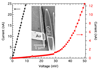
The CVD process results in CNTs of mixed chirality, so that both semiconducting as well as metallic tubes are in general expected to be present. Since the aim was to compare similar devices, we chose a growth temperature of C that yields mainly double-walled CNTs Spudat et al. (2009), and thus enhances the probability of fabricating metallic devices. All devices compared in this work showed linear current-voltage characteristics at room temperature, while at K a potential barrier becomes apparent, as one can see in Fig. 1. Note that while this data corresponds to one sample (device 6, cf. Tab. 1), it is in fact representative for all devices reported, although the height of the potential barrier varies between different devices. This intrinsic tunnel barrier is crucial for measuring a magnetoresistance effect in CNTs, because otherwise the spin polarization would be lost due to the conductivity mismatch Rashba (2000).
The interface between the ferromagnetic contact and the CNT is crucial for transport applications. To begin with, we note that the contact interface is quite small which is a consequence of the fact that DWCNTs have diameters of a few nanometers (cf. Tab. 1 for the diameters of the CNTs in the devices presented in this paper). Furthermore, since the injection of charge carriers occurs only at the point where the contact ends Tsukagoshi et al. (2002), the local magnetic environment has a strong influence on the MR measurements. Importantly, pinning and moving of domain walls in contacts that incorporate several magnetic domains leads to unstable switching behavior of the contacts and a non-trivial MR signal Morgan et al. (2013b). For this reason, we optimized the shape of the contacts in such a way that the magnetization is in-plane along the long axis with a single or at most two domains Morgan et al. (2013a). The magnetic field in all magnetoresistance measurements presented in this work is applied in direction of the long axis of the contacts unless specified otherwise.
All measurements discussed here were performed at a temperature of K unless specified otherwise. The substrate served as a back gate, and the back gate voltage was kept constant for all measurements on the same device, as the gate voltage can strongly influence the MR effect Sahoo et al. (2005); Man et al. (2006). In order to be able to compare the magnitude of the MR effect of different devices, measurements presented here were carried out in a regime where the current showed no, or only very weak, dependence on the back gate voltage.
III Results and Discussion
III.1 Temperature and bias dependence of the magnetoresistance
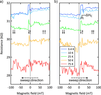
Figure 2 shows typical magnetoresistance (MR) measurements taken on a CoPd-contacted CNT in a temperature range from K up to K with a constant bias mV. For the sake of clarity, results for downward and upward field sweeps are plotted separately in (a) and (b). The data clearly reveals switching between low and high resistive states for parallel and antiparallel configuration of the magnetization directions of the contacts. As for all devices presented in this work, the MR effect is positive under the given circumstances. The overall resistance is shown to decrease with rising temperature, as expected for electrons tunneling through a barrier Likharev (1999), resulting in the offset observed between the curves. The MR signal decreases in magnitude along with the resistance, all in agreement with previous measurements on Fe-contacted CNTs Jensen et al. (2005). Along with the amplitude of the MR switching, the width of the feature is also reduced with increasing temperature from mT at K to mT at K. The width of the MR signal is determined by shape anisotropy, as the contacts are fabricated to have different lateral dimensions. The observed temperature-dependent change in width of the MR signal corresponds to a changing difference in coercive fields of the contacts. This behavior, in turn, correlates well with temperature-dependent SQUID data of CoPd Morgan et al. (2013a), which shows that at K, magnetoelastic anisotropy strongly affects the magnetization of nanocontact arrays, resulting in a lowered coercive field. This effect is different for the two contacts because of the interplay of shape anisotropy and magnetoelastic anisotropy. The reduced magnitude of the MR signal at elevated temperatures cannot be attributed to a decrease in magnetization of the CoPd contacts since their saturation magnetization is constant within this temperature range Morgan et al. (2013a). Therefore, this is a first indication that the MR effect is due to tunneling and we refer to it as TMR (tunneling magnetoresistance) in the following.
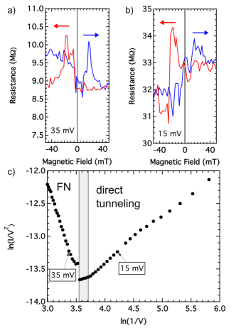
Figures 3(a) and 3(b) show MR measurements of another device at K using different bias voltages . Though the background of the traces and the details of the TMR switching vary from sweep to sweep and, in particular, between different thermal cycles, the coercive fields and the size of the MR effect observed remain the same. Introducing the definition of the size of the tunneling magnetoresistance effect
| (1) |
with () referring to the conductance in the parallel (antiparallel) magnetic configuration of the contacts, and averaging the backgrounds, we obtain TMR for the measurement with bias voltage mV [Fig. 3(a)] and TMR for the measurement with mV [Fig. 3(b)]. At first glance, this seems to contradict the general observation that the size of the MR effect in CNTs decreases with increasing bias voltage Zhao et al. (2002); Man et al. (2006). Interestingly, the plot shown in Fig. 3(c) reveals that the two measurements correspond to different tunneling regimes: the low-bias measurement corresponds to the direct tunneling regime, while the high-bias measurement corresponds to the Fowler-Nordheim (FN) tunneling regime foo . In the direct tunneling regime, the bias voltage applied is smaller than the average barrier height. On the other hand, in the case of FN tunneling, the bias voltage exceeds the average barrier height. As a consequence, the effective barrier width is reduced and the probability of tunneling enhanced. Usually, a plot is used to analyze FN tunneling through an oxide barrier Lenzlinger and Snow (1969). However, the double-logarithmic plot serves to emphasize the transition between the tunneling regimes as the change of slope becomes clearly visible Müller et al. (2009). Note that we do observe oscillations of the conductance with gate voltage at low bias voltage mV. In contrast to Man et al. Man et al. (2006), the data in this work are acquired at elevated bias voltage, where we do not observe strong oscillations of the conductance. The fact that we work with larger bias voltages is owed to comparably stronger tunnel barriers, which might also explain why in ref. [15] the MR signal vanishes at a bias voltage of 20 mV while our measurements show a large TMR signal at similar bias voltages.
A decreasing MR effect with increasing bias voltage is typical for conventional magnetic tunnel junctions and organic spin valve structures in the direct tunneling regime Moodera et al. (1995); Miyazaki and Tezuka (1995); Djayaprawira et al. (2005); Zhang et al. (2013). Spin-selective processes can play a role in the FN tunneling regime either due to band alignment Bowen et al. (2006) or trap assisted tunneling Qu et al. (2009) and lead to an increase in TMR Müller et al. (2009); Nagahama et al. (2007). Before we can understand how these effects might be influenced by the tunnel barrier between the metal contact and a carbon nanotube, we need to find a way to reliably characterize and understand the general influence of this tunnel barrier on the MR effect in CNTs. To exclude an influence of the bias voltage on the signal, we compare the TMR values of different CNT devices measured in the very narrow transition region between these two tunneling regimes, as represented by the gray shaded area in Fig. 3(c). This, of course, results in different absolute values of the applied bias voltage, since the conductances of the investigated devices differ. The absolute current through all the devices within this regime, however, was the same with nA.
III.2 Dependence of magnetoresistance on the strength of the tunnel barrier
| Device | CNT diameter (nm) | 1/G(KRT) (k) | 1/G(K) (k) | TMR (%) | |
|---|---|---|---|---|---|
| 1 | 5 | 35 | 30 | 0(0.5) | -0.1(+3) |
| 2 | 8 | 25 | 32 | 2(0.5) | 0.3(+4) |
| 3 | 1.6 | 150 | 210 | 5(0.75) | 0.40(+6) |
| 4 | 0.7 | 3700 | 11000 | 6.4(0.5) | 1.972(+3) |
| 5 | 3.2 | 1000 | 9000 | 12(2) | 8.00(+1) |
| 6 | 3 | 350 | 100000 | 15(1) | 24.71(+3) |
Table 1 lists the devices used for TMR measurements and it reveals that these devices differ significantly with respect to tube diameter and resistance. First of all, one should note that Pd contacts generally possess a high transmission, which is also known to increase with the diameter of the nanotube even for metallic CNTs Kim et al. (2005).
Indeed, the CoPd-contacted devices under investigation exhibit a similar behavior. Devices 1 and 2, characterized by the largest CNT diameters, show a high transmission, though the theoretical minimal value of the resistance for a single-wall CNT is not reached. A general trend can be observed that the value of the resistance at room temperature is inversely proportional to the CNT diameter. However, we note that the resistances of devices 5 and 6 appear to be too high compared to device 3. This deviation can be explained regarding the fact that most of the CNTs used in the present study are double-walled (DW) or even multiwalled, with device 4 being the only exception of a single-walled (SW) CNT. Though devices exhibiting metallic behavior were specifically selected, one should remember that DWCNTs can also be composed of outer semiconducting CNTs, with the inner tubes being metallic. Such a situation would manifest itself in a higher contact resistance and, in particular, as a higher device resistance in the case of our two-terminal device. Moreover, the strong increase in resistance with decreasing temperature supports this argument, as such a device should form a rather strong tunnel barrier. At low temperature, individual CNTs exhibit intrinsic tunnel barriers of different strength to metal contacts Bockrath et al. (1997), and this process depends largely on their chirality. Electrons experience a potential barrier at the contact-CNT interface as a result of local hybridization and a local dipolar moment Nemec et al. (2006); Shan and Cho (2004).
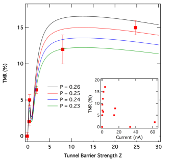
Figure 4 shows how the magnitude of the TMR signal changes with respect to the strength of the tunnel barrier formed between the CNT and the CoPd contacts. We define the dimensionless effective barrier strength of a device by directly comparing the resistance at K and at room temperature (RT) as follows (see also rightmost column of Table 1)
| (2) |
with K. Here, we assume that the change in resistance with temperature is dominated by tunnel barriers that are overcome at elevated temperature (K) by thermal activation of the charge carriers. This is valid, since all devices investigated exhibit relatively weak temperature dependence during cool-down before the tunnel barrier becomes visible at K. Physically, the dimensionless barrier strength describes the relation between the energy required to overcome the potential barrier and the kinetic (thermal) energy of electrons incident at the contact-CNT interface. We note that when an electron traverses the device it actually encounters two barriers, that is, when it enters and leaves a CNT. These are, however, experimentally indistinguishable and includes the overall effect of both tunnel barriers, though essentially is determined by the larger one. The normalization with respect to room temperature resistance allows for a direct comparison with the definition of the barrier strength in the model used to interpret our data (see below).
The data indicates that the tunnel barrier strength does indeed influence the magnitude of the TMR as suggested by Slonczewski for conventional TMR Slonczewski (1989), with devices characterized by low barriers unable to achieve an effect larger than a few %. Once the barrier reaches a certain strength, further increase will no longer affect the TMR. The inset of Fig. 4 shows a plot of TMR vs. current of the same devices that is usually used to analyze the performance of spin valves. Since this type of plot does not account for different tunnel barriers and bias voltage regimes, it is clear that for our devices a general trend cannot be expected.
To support our interpretation of the dependence of the TMR on the tunnel barrier strength, we compare our results to model calculations of the TMR for a CNT, approximated as a ballistic and noninteracting one-dimensional (gated) quantum wire Kane and Mele (1997); Egger and Gogolin (1998); Cottet et al. (2006a) interconnecting two ferromagnetic leads. In essence, such a model corresponds to an electronic interferometer studied previously both in experiment Liang et al. (2001); Sahoo et al. (2005); Man and Morpurgo (2005) and theoretically Cottet et al. (2006b, a). Here, the key element of the model, which has not been addressed so far in full detail, is the effect of the strength of tunnel barriers occurring at the CNT-lead interfaces on spin-dependent transport through the device. As the exact shape of each of the two tunnel barriers is unknown, we describe scattering of tunneling electrons at the CNT-lead interface by means of a repulsive Dirac-delta potential , the same at both ends of the CNT. This approach has already been proven sufficient to capture some key transport features of the interface for other material systems Blonder et al. (1982); Qi et al. (1998); Grundler (2001); Hu and Matsuyama (2001).
In general, within the scattering matrix approach the expression for linear-response conductance of a device at temperature takes the form Datta (1997); Blanter and Büttiker (2000)
| (3) |
where denotes the transmission coefficient for an electron of spin traversing a device through its th channel in the case when the spin moments of the leads are oriented parallel (P)/antiparallel (AP), and is the Fermi-Dirac distribution. Furthermore, we limit our considerations to the case of a CNT, which can support only two orbital channels () – a generic property inherited from graphene which stems from the presence of two inequivalent carbon atoms in a primitive cell Kane and Mele (1997); McEuen et al. (1999). Without losing generality, as long as one assumes two identical and uncoupled channels, a CNT can be approximated as a one-dimensional wire with for Cottet et al. (2006a). Next, the transmission coefficient is derived in a standard manner by means of the scattering matrix approach Datta (1997); Veillette et al. (2004); Cottet et al. (2006b),
| (4) |
with representing the square of the absolute value of the complex transmission amplitude. Note that when writing the equation above we assumed that both leads and interfaces (represented by the parameter ) are identical. The action of the magnetic configuration index on a spin index is defined as and , where one should understand the notation as and . In the absence of a magnetic field, the phase factor consists of two terms: first, , corresponding to the quantum-mechanical phase acquired by a free electron propagating with a wave vector in a wire of length , and second, , representing the spin-dependent phase shift Cottet et al. (2006b) gained by an electron when it is scattered at the interface back into the wire. If the electrostatic potential energy of the gated wire is small relative to its Fermi energy , one gets , where energy is defined relative to the Fermi level, m-1 is a typical value of the Fermi wave vector for electrons in a SWCNT Liang et al. (2001) and m/s its Fermi velocity.
Using standard quantum mechanical methods, and noting that in the low bias voltage limit only electrons in the vicinity of the Fermi level of the contacts participate in tunneling, one obtains Misiorny and Meyer (2016)
| (5) |
and
| (6) |
Here, the spin-dependent wave vector of free electrons in the leads, , is parameterized by the Fermi energy (assumed here eV) of the contacts, and the spin-polarization coefficient defined as Qi et al. (1998) , with . Furthermore, and with is the dimensionless barrier strength, defined as the ratio of the potential energy of the barrier and the energy of incident electrons from the Fermi level of the contacts, so that it is related to the experimental definition of the barrier strength, Eq. (2), as . In consequence, it can be noticed that the only two free parameters of the model are and .
The fit of the theoretical model to the experimental data points for a specific value of and different degrees of spin polarization of the contacts is shown as solid lines in Fig. 4. The value of was chosen so that it matched the experimental finding of only positive values for the MR effect for small . It is to some extent arbitrary, since the MR shows an oscillatory behavior with . Moreover, the temperature used for the fit is K, and the length of the CNT is taken as nm. Though both these values deviate slightly from those observed in the experiment, they yield better fits. Nevertheless, this seems reasonable, since, first, lithography of various devices is usually not exact, so that it is expected that they are characterized by a somewhat different CNT length, and, second, for a given value of and large the model is sensitive to the interplay of values of temperature and length Misiorny and Meyer (2016).
Comparing the results of the calculations and the experimental data, we find that the spin polarization of the charge carriers injected from the CoPd contacts is . This is rather large compared to CNTs contacted with NiPd, where the spin polarization was estimated to be % Man et al. (2006). Nevertheless, this is a very reasonable value considering the fact that the polarization of charge carriers injected from pure Co has been found to be between and Tedrow and Meservey (1973) combined with the relatively large polarization of Pd induced by Co Shan et al. (1993). Furthermore, the model is based on a single transport channel while most of the CNTs used in the devices contain two walls and thus likely more transport channels. While the qualitative effect remains unchanged if more channels are included in the model Misiorny and Meyer (2016), this might result in a deviation of the contact polarization. On the other hand, interaction between a CNT and contacts can block channels in a CNT with more than one wall Ranjan et al. (2004) and cancel contributions from other channels. The good agreement of the experimental data with the model further proves the importance of the tunnel barrier strength in optimizing TMR in a CNT-based device.
The fact that the nature and the strength of the barrier significantly affect the TMR signal has been observed in ”classical” metallic tunnel junctions (MTJs) with MgO as the insulating barrier. Generally, the TMR effect increases with increasing MgO thickness Yuasa et al. (2004). However, pronounced oscillations are observed in MTJs with Heusler alloys Marukame et al. (2010); Wang et al. (2010) or Fe Yuasa et al. (2004) as the contact material. This is usually attributed to different wave vectors of the and the band of MgO at the Fermi level that lead to interference effects Butler et al. (2001). Investigations of graphene spin valves, on the other hand, suggest a monotonic increase of the MR and saturation for strong barriers Dlubak et al. (2012). Moreover, the rather small TMR signal previously found in CNT spin valves with permalloy contacts and the small contact polarization deduced using Julière’s model Aurich et al. (2010) might in fact be explained with a weak tunnel barrier in the framework of our model.
Finally, it should be pointed out that although the proposed model describes the experimental results relatively well, one should still bear in mind its limitations. The model assumes free (s-band) electrons in the contacts, and the CNT-contact interface is approximated by a Dirac-delta potential. In reality, the energy barrier at the interface can be much more complex, with a potential profile depending on many factors, such as the interface roughness or adsorbates. Also, the free-electron model should be applied to transition metals and their alloys with great care, as in principle one should expect a more complicated band structure to be responsible for electron tunneling Zhang and Levy (1999). To account for all these details a model from first principles should be developed Mavropoulos et al. (2004), a task which is way beyond the scope of the present paper.
Within these limitations, it is nevertheless obvious that the tunnel barrier has a significant effect on the TMR found in CNT spin valves. Furthermore, CoPd-CNT devices form sufficiently low barriers that the addition of tunnel barriers from spin selective insulators becomes feasible. This would also enable one to study the FN tunneling regime more closely, which may can lead to significantly larger TMR values.
III.3 Spin precession within carbon nanotubes
As the results discussed above correspond to local measurements, there is the possibility of several spurious effects, such as the Hall effect, anisotropic magnetoresistance (AMR) Tombros et al. (2006), or other ohmic effects Man and Morpurgo (2005) influencing the magnetotransport. One important contribution to the local MR signal can be caused by the magneto-Coulomb effect Ono et al. (1998); Shimada et al. (2003); van der Molen et al. (2006). However, the measurements presented in this work are not taken in the Coulomb blockade regime. For this reason, the influence of the magneto-Coulomb effect should be weak at least. Another effect is the tunneling anisotropic magnetoresistance (TAMR), which can completely mimic the MR effect Gould et al. (2004). TAMR is an effect solely related to the anisotropic density of states in the ferromagnetic contacts and is usually found in materials with strong spin-orbit coupling that lack inversion symmetry and show AMR, like lanthanum strontium manganite (LSMO) Grünewald et al. (2011). Though we measure no significant AMR in our CoPd contacts, TAMR might be related to the barrier, as shown for fcc Co(111) contacts on Al2O3 Wang et al. (2013). Since our contacts have a similar structure Morgan et al. (2013a), and the exact nature of the barrier in our devices is unknown, we have to make sure that spin polarized charge carriers are indeed injected into the CNTs.
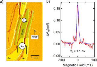
To prove spin injection into and spin precession within the CNTs, Hanle measurements were performed on a device with a nonlocal three-terminal configuration. Figure 5(a) presents an atomic force microscope image (AFM) of a device prepared for nonlocal measurements, in which a nonlocal voltage is measured along a separate path from the applied current, using three contacts as indicated. The device displayed a local TMR signal of 15% and thus, is an example for the strong barrier case as discussed above. For the Hanle measurements, all contacts are magnetized in-plane in the same direction. The sample is then rotated at zero applied field. Subsequently, a magnetic field is applied perpendicular to the plane, which leaves the magnetization of the contacts unaffected due to the shape anisotropy Morgan et al. (2013a). The resulting Hanle signal is presented in Fig. 5(b). Note that this signal was recorded at a bias of nA and thus outside the Coulomb blockade regime. The voltage difference measured between the injector and the detector contact at is due to an imbalance of the electrochemical potentials, and , of spin-up and spin-down electrons, respectively. It is reduced as the spins dephase while precessing about the perpendicular magnetic field with the Larmor frequency . The data is fitted with a Lorentzian peak (blue line), and the magnetic field at the full width at half maximum of the peak is measured to be approximately mT. Following Ref. Dash et al. (2009), where is the spin lifetime. Taking the g-factor g = 2 for a CNT in a perpendicularly applied magnetic field Cobden et al. (1998), we obtain ns. This is a lower bound for the spin coherence time , since the Hanle effect in combination with spin injection probes the (coherent) dephasing of the conduction electrons Žutić et al. (2004). The value of is directly related to the spin accumulation , with TSP denoting the tunneling spin polarization of the ferromagnet-barrier interface of 0.24 as obtained in the previous section, which yields meV. This value is rather large and of similar magnitude to the one found in Si-based spin valves at room temperature Dash et al. (2009). The spin lifetime is long compared to the spin lifetime of ns typically found in graphene lateral spin valves on substrates Han and Kawakami (2011); Avsar et al. (2011). Only very recently, lifetimes of nanoseconds were reported in high mobility graphene devices sandwiched in hBN Guimarães et al. (2014) and in suspended graphene devices covered with a layer of BN Drögeler et al. (2014).
As discussed above, our CNT lateral spin valves compete very well with state-of-the-art silicon or graphene based devices. Because the performance of devices considered in this paper relies on the tunnel barrier that forms intrinsically between the metal contact and the CNT, the measurements have to be conducted at low temperatures. On the other hand, the spin lifetime in graphene devices is known to exhibit no, or only very little temperature dependence Avsar et al. (2011). Since we now understand the influence of the tunnel barrier in CNT-based devices, tunnel barrier engineering becomes possible. Spin selective insulators like EuO can be used to increase the temperature for spin injection. The spin lifetime is very likely still influenced by charge traps in the SiO2. Suspending the CNTs or low dose gamma irradiation, which is known to remove traps in the oxide and to improve the performance of CNT-based field-effect transistors Sydoruk et al. (2014), would be expected to enhance the spin lifetime. The diameter of the CNT used for the Hanle measurements was nm, giving rise to a spin-orbit coupling strength in the order of meV Kuemmeth et al. (2008). Since spin-orbit coupling is another source of decoherence, using CNTs with larger diameter might increase the spin lifetime as well. Recently, a coherence time of ns was found in a CNT-based double quantum dot coherently coupled to microwave cavity photons Viennot et al. (2015) that indicates the potential of the spin coherence in CNT spin valves. However, electron spin resonance suggests that the electron-electron interactions in a Tomonaga-Luttinger liquid might severely reduce the spin coherence time of one-dimensional metallic devices Dóra et al. (2008). Hanle measurements on improved devices will advance quantitative understanding of spin relaxation properties of CNTs.
IV Conclusion
In this article, we analyzed the TMR effect in lateral spin valve devices based on CNTs. We showed that the strength of the tunnel barrier forming intrinsically between ferromagnetic contacts made out of CoPd and CNTs has a significant influence on the size of the TMR signal. Approximating a CNT as a ballistic and noninteracting one-dimensional quantum wire, we modeled the experimental data and found that the spin polarization of the injected electrons is about 24%, and that the TMR effect exhibits a non-monotonic dependence on the barrier strength. Importantly, the usage of CoPd as the contact material allowed for achieving rather high transmission coefficients, with great perspectives for further optimization of the properties of the barrier, for instance by introducing spin-selective insulators. Moreover, Hanle measurements in a nonlocal three-terminal configuration served to confirm the injection of spin-polarized electrons into a CNT. In particular, spin accumulation and spin lifetime extracted from the Hanle effect turned out to be of similar magnitude as in state-of-the-art spin valve devices based on Si or graphene. Our study provides a deeper understanding of the barrier dependence of the TMR in CNTs, facilitating the development of applications of this one-dimensional material in spintronic devices.
Acknowledgements.
The authors thank S. Trellenkamp for e-beam writing, T. Jansen for metalization, and N. Schnitzler, H. Kertz and H. Pfeifer for technical assistance with the cryostat setups. We thank D. Bürgler, G. Schmidt, and P. Mavropoulos for fruitful discussions. The WSxM software was used to analyze all AFM data Horcas et al. (2007). M.M. acknowledges financial support from the Alexander von Humboldt Foundation and the Polish Ministry of Science and Higher Education through a young scientist fellowship (0066/E-336/9/2014). C. Meyer acknowledges financial support from the DFG Research unit FOR912.References
- Žutić et al. (2004) I. Žutić, J. Fabian, and S. Das Sarma, “Spintronics: Fundamentals and applications,” Rev. Mod. Phys. 76, 323–410 (2004).
- Han et al. (2014) W. Han, R. K. Kawakami, M. Gmitra, and J. Fabian, “Graphene spintronics,” Nat. Nanotechnol. 9, 794–807 (2014).
- Drögeler et al. (2014) M. Drögeler, F. Volmer, M. Wolter, B. Terrés, K. Watanabe, T. Taniguchi, G. Güntherodt, C. Stampfer, and B. Beschoten, “Nanosecond spin lifetimes in single-and few-layer graphene–hBN heterostructures at room temperature,” Nano Lett. 14, 6050–6055 (2014).
- Dlubak et al. (2012) B. Dlubak, M-B. Martin, C. Deranlot, B. Servet, S. Xavier, R. Mattana, M. Sprinkle, C. Berger, W. A. DeHeer, F. Petroff, A. Anane, P. Seneor, and A. Fert, “Highly efficient spin transport in epitaxial graphene on SiC,” Nat. Phys. 8, 557–561 (2012).
- Tombros et al. (2007) N. Tombros, C. Jozsa, M. Popinciuc, H. T. Jonkman, and B. J. van Wees, “Electronic spin transport and spin precession in single graphene layers at room temperature,” Nature 448, 571 (2007).
- Han et al. (2010) W. Han, K. Pi, K. M. McCreary, Y. Li, J. J. I. Wong, A. G. Swartz, and R. K. Kawakami, “Tunneling spin injection into single layer graphene,” Phys. Rev. Lett. 105, 167202 (2010).
- Kamalakar et al. (2014) M. V. Kamalakar, A. Dankert, J. Bergsten, T. Ive, and S. P. Dash, “Enhanced Tunnel Spin Injection into Graphene using Chemical Vapor Deposited Hexagonal Boron Nitride,” Sci. Rep. 4, 6146 (2014).
- T. et al. (1999) Kazuhito T., Bruce W. A., and Hiroki A., “Coherent transport of electron spin in a ferromagnetically contacted carbon nanotube,” Nature 401, 572 (1999).
- Mann et al. (2003) D. Mann, A. Javey, J. Kong, Q. Wang, and H. Dai, “Ballistic transport in metallic nanotubes with reliable pd ohmic contacts,” Nano Lett. 3, 1541–1544 (2003).
- Zhao et al. (2002) B. Zhao, I. Mönch, H. Vinzelberg, T. Mühl, and C.M. Schneider, “Spin-coherent transport in ferromagnetically contacted carbon nanotubes,” Appl. Phys. Lett. 80, 3144–3146 (2002).
- Jensen et al. (2005) A. Jensen, J.R. Hauptmann, J. Nygård, and P.E. Lindelof, “Magnetoresistance in ferromagnetically contacted single-wall carbon nanotubes,” Phys. Rev. B 72, 035419 (2005).
- Samm et al. (2014) J. Samm, J. Gramich, A. Baumgartner, M. Weiss, and C. Schönenberger, “Optimized fabrication and characterization of carbon nanotube spin valves,” J. Appl. Phys. 115, 174309 (2014).
- Dirnaichner et al. (2015) A. Dirnaichner, M. Grifoni, A. Prüfling, D. Steininger, A.K. Hüttel, and C. Strunk, “Transport across a carbon nanotube quantum dot contacted with ferromagnetic leads: Experiment and nonperturbative modeling,” Phys. Rev. B 91, 195402 (2015).
- Sahoo et al. (2005) S. Sahoo, T. Kontos, J. Furer, C. Hoffmann, M. Gräber, A. Cottet, and C. Schönenberger, “Electric field control of spin transport,” Nat. Phys. 1, 99–102 (2005).
- Man et al. (2006) H.T. Man, I.J.W. Wever, and A.F. Morpurgo, “Spin-dependent quantum interference in single-wall carbon nanotubes with ferromagnetic contacts,” Phys. Rev. B 73, 241401 (2006).
- Zólyomi et al. (2008) V. Zólyomi, J. Koltai, Á. Rusznyák, J. Kürti, Á. Gali, F. Simon, H. Kuzmany, Á. Szabados, and P. R. Surján, “Intershell interaction in double walled carbon nanotubes: Charge transfer and orbital mixing,” Phys. Rev. B 77, 245403 (2008).
- Koshino et al. (2015) M. Koshino, P. Moon, and Y.-W. Son, “Incommensurate double-walled carbon nanotubes as one-dimensional moiré crystals,” Phys. Rev. B 91, 035405 (2015).
- Kong et al. (1998) J. Kong, H. T. Soh, A. M. Cassell, C. F. Quate, and H. J. Dai, “Synthesis of individual single-walled carbon nanotubes on patterned silicon wafers,” Nature 395, 878–881 (1998).
- Feuillet-Palma et al. (2010) C. Feuillet-Palma, T. Delattre, P. Morfin, J.-M. Berroir, G. Fève, D. C. Glattli, B. Plaçais, A. Cottet, and T. Kontos, “Conserved spin and orbital phase along carbon nanotubes connected with multiple ferromagnetic contacts,” Phys. Rev. B 81, 115414 (2010).
- Preusche et al. (2009) D. Preusche, S. Schmidmeier, E. Pallecchi, C. Dietrich, A.K. Hüttel, J. Zweck, and C. Strunk, “Characterization of ferromagnetic contacts to carbon nanotubes,” J. Appl. Phys. 106, 084314 (2009).
- Morgan et al. (2012) C. Morgan, C.M. Schneider, and C. Meyer, “Permalloy and Co50Pd50 as ferromagnetic contacts for magnetoresistance measurements in carbon nanotube-based transport structures,” J. Appl. Phys. 111, 07B309 (2012).
- Morgan et al. (2013a) C. Morgan, K. Schmalbuch, F García-Sánchez, C.M. Schneider, and C. Meyer, “Structure and magnetization in CoPd thin films and nanocontacts,” J. Magn. Magn. Mater. 325, 112–116 (2013a).
- Spudat et al. (2009) C. Spudat, C. Meyer, K. Goss, and C.M. Schneider, “Peapod synthesis depending on the number of nanotube sidewalls,” Phys. Status Solidi B 246, 2498–2501 (2009).
- Rashba (2000) E. I. Rashba, “Theory of electrical spin injection: Tunnel contacts as a solution of the conductivity mismatch problem,” Phys. Rev. B 62, R16267–R16270 (2000).
- Tsukagoshi et al. (2002) K. Tsukagoshi, N. Yoneya, S. Uryu, Y. Aoyagi, A. Kanda, Y. Ootuka, and B.W. Alphenaar, “Carbon nanotube devices for nanoelectronics,” Physica B 323, 107–114 (2002).
- Morgan et al. (2013b) C. Morgan, D. Metten, C. M. Schneider, and C. Meyer, “Effect of contact geometry on magnetoresistance in copd-contacted carbon nanotubes,” Phys. Status Solidi B 250, 2622–2626 (2013b).
- Likharev (1999) K.K. Likharev, “Single-electron devices and their applications,” Proc. IEEE 87, 606–632 (1999).
- (28) The“jump” that appears between the transition regime and the FN regime is caused by a internal switching of measurement ranges in the Keithley 2636B at a current of nA. It does not affect the qualitative shape of the curve (cf. Fig. 1).
- Lenzlinger and Snow (1969) M. Lenzlinger and E. H. Snow, “Fowler-Nordheim tunneling into thermally grown SiO2,” J. Appl. Phys. 40, 278–283 (1969).
- Müller et al. (2009) M. Müller, G.-X. Miao, and J.S. Moodera, “Exchange splitting and bias-dependent transport in EuO spin filter tunnel barriers,” Europhys. Lett. 88, 47006 (2009).
- Moodera et al. (1995) J.S. Moodera, L.R. Kinder, T.M. Wong, and R. Meservey, “Large magnetoresistance at room temperature in ferromagnetic thin film tunnel junctions,” Phys. Rev. Lett. 74, 3273–3276 (1995).
- Miyazaki and Tezuka (1995) T. Miyazaki and N. Tezuka, “Giant magnetic tunneling effect in Fe/Al2O3/Fe junction ,” J. Magn. Magn. Mater. 139, L231 – L234 (1995).
- Djayaprawira et al. (2005) D.D. Djayaprawira, K. Tsunekawa, M. Nagai, H. Maehara, S. Yamagata, N. Watanabe, S. Yuasa, Y. Suzuki, and K. Ando, “230% room-temperature magnetoresistance in CoFeB/MgO/CoFeB magnetic tunnel junctions,” Appl. Phys. Lett. 86, 092502 (2005).
- Zhang et al. (2013) X. Zhang, S. Mizukami, T. Kubota, Q. Ma, M. Oogane, H. Naganuma, Y. Ando, and T. Miyazaki, “Observation of a large spin-dependent transport length in organic spin valves at room temperature,” Nat. Commun. 4, 1392 (2013).
- Bowen et al. (2006) M. Bowen, A. Barthélémy, V. Bellini, M. Bibes, P. Seneor, E. Jacquet, J.-P. Contour, and P.H. Dederichs, “Observation of Fowler-Nordheim hole tunneling across an electron tunnel junction due to total symmetry filtering,” Phys. Rev. B 73, 140408 (2006).
- Qu et al. (2009) T.L. Qu, J. Li, Y.G. Zhao, J.W. Mei, X. Liu, H.F. Tian, J.P. Shi, S.M. Guo, J. Li, D.N. Zheng, and J.Q. Li, “Nonlinear current-voltage behavior and giant positive magnetoresistance in nonmagnetic Au/Yttria-stabilized zirconia/Si heterostructures,” Appl. Phys. Lett. 95, 242113 (2009).
- Nagahama et al. (2007) T. Nagahama, T.S. Santos, and J.S. Moodera, “Enhanced magnetotransport at high bias in quasimagnetic tunnel junctions with EuS spin-filter barriers,” Phys. Rev. Lett. 99, 016602 (2007).
- Kim et al. (2005) W. Kim, A. Javey, R. Tu, J. Cao, Q. Wang, and H.J. Dai, “Electrical contacts to carbon nanotubes down to 1 nm in diameter,” Appl. Phys. Lett. 87, 173101 (2005).
- Bockrath et al. (1997) M. Bockrath, D.H. Cobden, P.L. McEuen, N.G. Chopra, A. Zettl, A. Thess, and R.E. Smalley, “Single-electron transport in ropes of carbon nanotubes,” Science 275, 1922–1925 (1997).
- Nemec et al. (2006) N. Nemec, D. Tománek, and G. Cuniberti, “Contact dependence of carrier injection in carbon nanotubes: An ab initio study,” Phys. Rev. Lett. 96, 076802 (2006).
- Shan and Cho (2004) B. Shan and K. Cho, “Ab initio study of Schottky barriers at metal-nanotube contacts,” Phys. Rev. B 70, 233405 (2004).
- Slonczewski (1989) J.C. Slonczewski, “Conductance and exchange coupling of two ferromagnets separated by a tunneling barrier,” Phys. Rev. B 39, 6995–7002 (1989).
- Kane and Mele (1997) C.L. Kane and E.J. Mele, “Size, shape, and low energy electronic structure of carbon nanotubes,” Phys. Rev. Lett. 78, 1932 (1997).
- Egger and Gogolin (1998) R. Egger and A.O. Gogolin, “Correlated transport and non-fermi-liquid behavior in single-wall carbon nanotubes,” Eur. Phys. J. B 3, 281–300 (1998).
- Cottet et al. (2006a) A. Cottet, T. Kontos, S. Sahoo, H.T. Man, M.-S. Choi, W. Belzig, C. Bruder, A.F. Morpurgo, and C. Schönenberger, “Nanospintronics with carbon nanotubes,” Sem. Sci. Tech. 21, S78 (2006a).
- Liang et al. (2001) W. Liang, M. Bockrath, D. Bozovic, J.H. Hafner, M. Tinkham, and H. Park, “Fabry-Pérot interference in a nanotube electron waveguide,” Nature 411, 665–669 (2001).
- Man and Morpurgo (2005) H.T. Man and A.F. Morpurgo, “Sample-specific and ensemble-averaged magnetoconductance of individual single-wall carbon nanotubes,” Phys. Rev. Lett. 95, 026801 (2005).
- Cottet et al. (2006b) A. Cottet, T. Kontos, W. Belzig, C. Schönenberger, and C. Bruder, “Controlling spin in an electronic interferometer with spin-active interfaces,” Europhys. Lett. 74, 320–326 (2006b).
- Blonder et al. (1982) G.E. Blonder, M. Tinkham, and T.M. Klapwijk, “Transition from metallic to tunneling regimes in superconducting microconstrictions: Excess current, charge imbalance, and supercurrent conversion,” Phys. Rev. B 25, 4515–4532 (1982).
- Qi et al. (1998) Y. Qi, D.Y. Xing, and J. Dong, “Relation between Julliere and Slonczewski models of tunneling magnetoresistance,” Phys. Rev. B 58, 2783–2787 (1998).
- Grundler (2001) D. Grundler, “Oscillatory spin-filtering due to gate control of spin-dependent interface conductance,” Phys. Rev. Lett. 86, 1058 (2001).
- Hu and Matsuyama (2001) C.-M. Hu and T. Matsuyama, “Spin injection across a heterojunction: A ballistic picture,” Phys. Rev. Lett. 87, 066803 (2001).
- Datta (1997) S. Datta, Electronic transport in mesoscopic systems (Cambridge University Press, Cambridge, 1997).
- Blanter and Büttiker (2000) Ya.M. Blanter and M. Büttiker, “Shot noise in mesoscopic conductors,” Phys. Rep. 336, 1–166 (2000).
- McEuen et al. (1999) P.L. McEuen, M. Bockrath, D.H. Cobden, Y.-G. Yoon, and S.G. Louie, “Disorder, pseudospins, and backscattering in carbon nanotubes,” Phys. Rev. Lett. 83, 5098 (1999).
- Veillette et al. (2004) M.Y. Veillette, C. Bena, and L. Balents, “Spin precession and oscillations in mesoscopic systems,” Phys. Rev. B 69, 075319 (2004).
- Misiorny and Meyer (2016) M. Misiorny and C Meyer, in preparation (2016).
- Tedrow and Meservey (1973) P.M. Tedrow and R. Meservey, “Spin polarization of electrons tunneling from films of Fe, Co, Ni, and Gd,” Phys. Rev. B 7, 318–326 (1973).
- Shan et al. (1993) Z.-S. Shan, Ping He, C. Moore, John Woollam, and D. J. Sellmyer, “Behavior of disordered Co-Pd, Co-Ag, and Co-Mo alloys in multilayer interfaces,” J. Appl. Phys. 73, 6057–6059 (1993).
- Ranjan et al. (2004) N. Ranjan, R. Gutiérrez, S. Krompiewski, and G. Cuniberti, “Electron transport in carbon nanotube-metal system: contact effects,” Mol. Phys. Rep. 40, 125–130 (2004).
- Yuasa et al. (2004) S. Yuasa, T. Nagahama, A. Fukushima, Y. Suzuki, and K. Ando, “Giant room-temperature magnetoresistance in single-crystal Fe/MgO/Fe magnetic tunnel junctions,” Nat. Mater. 3, 868–871 (2004).
- Marukame et al. (2010) T. Marukame, T. Ishikawa, T. Taira, K. Matsuda, T. Uemura, and M. Yamamoto, “Giant oscillations in spin-dependent tunneling resistances as a function of barrier thickness in fully epitaxial magnetic tunnel junctions with a MgO barrier,” Phys. Rev. B 81, 134432 (2010).
- Wang et al. (2010) W. Wang, E. Liu, M. Kodzuka, H. Sukegawa, M. Wojcik, E. Jedryka, G. H. Wu, K. Inomata, S. Mitani, and K. Hono, “Coherent tunneling and giant tunneling magnetoresistance in Co2FeAl/MgO/CoFe magnetic tunneling junctions,” Phys. Rev. B 81, 140402 (2010).
- Butler et al. (2001) W. H. Butler, X.-G. Zhang, T. C. Schulthess, and J. M. MacLaren, “Spin-dependent tunneling conductance of sandwiches,” Phys. Rev. B 63, 054416 (2001).
- Aurich et al. (2010) H. Aurich, A. Baumgartner, F. Freitag, A. Eichler, J. Trbovic, and C. Schönenberger, “Permalloy-based carbon nanotube spin-valve,” App. Phys. Lett. 97, 153116 (2010).
- Zhang and Levy (1999) S. Zhang and P.M. Levy, “Models for magnetoresistance in tunnel junctions,” Eur. Phys. J. B 10, 599–606 (1999).
- Mavropoulos et al. (2004) P. Mavropoulos, N. Papanikolaou, and P.H. Dederichs, “Korringa-Kohn-Rostoker Green-function formalism for ballistic transport,” Phys. Rev. B 69, 125104 (2004).
- Tombros et al. (2006) N. Tombros, S.J. van der Molen, and B.J. van Wees, “Separating spin and charge transport in single-wall carbon nanotubes,” Phys. Rev. B 73, 233403 (2006).
- Ono et al. (1998) K. Ono, H. Shimada, and Y. Ootuka, “Spin polarization and Magneto-Coulomb oscillations in ferromagnetic single electron devices,” J. Phys. Soc. Jpn. 67, 2852–2856 (1998).
- Shimada et al. (2003) H. Shimada, K. Ono, and Y. Ootuka, “Driving the single-electron device with a magnetic field (invited),” J. Appl. Phys. 93, 8259–8264 (2003).
- van der Molen et al. (2006) S.J. van der Molen, N. Tombros, and B.J. van Wees, “Magneto-coulomb effect in spin-valve devices,” Phys. Rev. B 73, 220406 (2006).
- Gould et al. (2004) C. Gould, C. Rüster, T. Jungwirth, E. Girgis, G.M. Schott, R. Giraud, K. Brunner, G. Schmidt, and L.W. Molenkamp, “Tunneling anisotropic magnetoresistance: A spin-valve-like tunnel magnetoresistance using a single magnetic layer,” Phys. Rev. Lett. 93, 117203 (2004).
- Grünewald et al. (2011) M. Grünewald, M. Wahler, F. Schumann, M. Michelfeit, C. Gould, R. Schmidt, F. Würthner, G. Schmidt, and L.W. Molenkamp, “Tunneling anisotropic magnetoresistance in organic spin valves,” Phys. Rev. B 84, 125208 (2011).
- Wang et al. (2013) K. Wang, T.L.A. Tran, P. Brinks, J.G.M. Sanderink, T. Bolhuis, W.G. van der Wiel, and M.P. de Jong, “Tunneling anisotropic magnetoresistance in Co/AlOx/Al tunnel junctions with fcc Co (111) electrodes,” Phys. Rev. B 88, 054407 (2013).
- Dash et al. (2009) S.P. Dash, S. Sharma, R.S. Patel, M.P. de Jong, and R. Jansen, “Electrical creation of spin polarization in silicon at room temperature,” Nature 462, 491–494 (2009).
- Cobden et al. (1998) D.H. Cobden, M. Bockrath, P.L. McEuen, A.G. Rinzler, and R.E. Smalley, “Spin splitting and even-odd effects in carbon nanotubes,” Phys. Rev. Lett. 81, 681–684 (1998).
- Han and Kawakami (2011) W. Han and R.K. Kawakami, “Spin relaxation in single-layer and bilayer graphene,” Phys. Rev. Lett. 107, 047207 (2011).
- Avsar et al. (2011) A. Avsar, T.-Y. Yang, S. Bae, J. Balakrishnan, F. Volmer, M. Jaiswal, Z. Yi, S.R. Ali, G. Güntherodt, B.H. Hong, B. Beschoten, and B. Özyilmaz, “Toward wafer scale fabrication of graphene based spin valve devices,” Nano Lett. 11, 2363–2368 (2011).
- Guimarães et al. (2014) M.H.D. Guimarães, P.J. Zomer, J. Ingla-Aynés, J.C. Brant, N. Tombros, and B.J. van Wees, “Controlling spin relaxation in hexagonal BN-encapsulated graphene with a transverse electric field,” Phys. Rev. Lett. 113, 086602 (2014).
- Sydoruk et al. (2014) V.A. Sydoruk, K. Goß, C. Meyer, M.V. Petrychuk, B.A. Danilchenko, P. Weber, C. Stampfer, J. Li, and S.A.s Vitusevich, “Low-frequency noise in individual carbon nanotube field-effect transistors with top, side and back gate configurations: effect of gamma irradiation,” Nanotechnology 25, 035703 (2014).
- Kuemmeth et al. (2008) F. Kuemmeth, S. Ilani, D. C. Ralph, and P. L. McEuen, “Coupling of spin and orbital motion of electrons in carbon nanotubes,” Nature 452, 06822 (2008).
- Viennot et al. (2015) J. J. Viennot, M. C. Dartiailh, A. Cottet, and T. Kontos, “Coherent coupling of a single spin to microwave cavity photons,” Science 349, 408–411 (2015).
- Dóra et al. (2008) B. Dóra, M. Gulácsi, J. Koltai, V. Zólyomi, J. Kürti, and F. Simon, “Electron spin resonance signal of luttinger liquids and single-wall carbon nanotubes,” Phys. Rev. Lett. 101, 106408 (2008).
- Horcas et al. (2007) I. Horcas, R. Fernández, J.M. Gómez-Rodríiguez, J. Colchero, J. Gómez-Herrero, and A.M. Baro, “WSXM: A software for scanning probe microscopy and a tool for nanotechnology,” Rev. Sci. Instrum. 78, 013705 (2007).