Spatial control of laser-induced doping profiles in graphene on hexagonal boron nitride
Abstract
We present a method to create and erase spatially resolved doping profiles in graphene-hexagonal boron nitride (hBN) heterostructures. The technique is based on photo-induced doping by a focused laser and does neither require masks nor photo resists. This makes our technique interesting for rapid prototyping of unconventional electronic device schemes, where the spatial resolution of the rewritable, long-term stable doping profiles is only limited by the laser spot size ( 600 nm) and the accuracy of sample positioning. Our optical doping method offers a way to implement and to test different, complex doping patterns in one and the very same graphene device, which is not achievable with conventional gating techniques.
keywords:
Graphene, p-n junction, electric transport, boron nitride, photo-induced doping, laserPeter Grünberg Institute (PGI-9), Forschungszentrum Jülich, 52425 Jülich, Germany \alsoaffiliationPhysics and Materials Science Research Unit, Université du Luxembourg, 1511 Luxembourg, Luxembourg \alsoaffiliationPeter Grünberg Institute (PGI-9), Forschungszentrum Jülich, 52425 Jülich, Germany \alsoaffiliationPeter Grünberg Institute (PGI-9), Forschungszentrum Jülich, 52425 Jülich, Germany \alsoaffiliationPeter Grünberg Institute (PGI-9), Forschungszentrum Jülich, 52425 Jülich, Germany \abbreviationsGr,hBN,CNP
![[Uncaptioned image]](/html/1511.00500/assets/x1.png)
In recent years, the stacking of two-dimensional materials bound by van der Waals interaction has emerged as an interesting approach for designing and studying novel device concepts for electronic 1, 2, 3, 4 and optoelectronic applications 5, 6, 7. In particular, material stacks built around graphene (Gr) promise interesting electronic properties 8, 9, 10, 11, 12 and many possibilities for hosting high-quality devices. Different two-dimensional materials have been shown to be favorable substrates for graphene in such stacks 13. Most prominently, hexagonal boron nitride (hBN) has been used in numerous studies to encapsulate graphene and enable high-quality graphene devices 14, 15, 16, 11, 17. In order to enable functional electronic devices, local gates are usually used to implement p-n junctions or other doping profiles. Recently, an alternative way has been reported for changing the charge carrier doping in hBN-Gr stacks by optical illumination 18. Notably this photo-induced doping in heterostructures of graphene and hBN 18 is significantly more efficient than for graphene on SiO2 19, 20. Here we show that a focused laser can be used to create charge doping patterns, such as lateral p-n junctions, with high spatial precision and long lifetimes in Gr-hBN heterostructures. Importantly the presented laser-induced doping technique works completely without masks and photo-resists. We show that the lateral resolution is essentially only limited by the laser spot size and accuracy of sample positioning. The process maintains the high electronic mobility of the graphene sample and offers distinct advantages over conventional gate electrodes, such as rewritability, the possibility of changing and controlling doping profiles in a single device, and a reduction of process steps. This makes our findings highly interesting for prototyping unconventional electronic device schemes based on graphene.
Our sample consists of a single-layer graphene sheet which is encapsulated by two multi-layer hBN flakes. This material stack is obtained by a dry and resist-free transfer process, which has been shown to result in high-mobility graphene devices 9, 10, 21. The resulting heterostructure is placed on a highly doped silicon substrate with a 285 nm thick SiO2 layer (Figure 1a). The sample is structured into a Hall bar using electron beam lithography and reactive ion etching. Finally, it is contacted via chrome/gold electrodes on the sides of the heterostructure 9. The width of the Hall bar is 1.9 µm and the total length is 12.3 µm. For transport measurements, we use a four-probe geometry with a constant source-drain current of 50 nA (Figure 1b). The longitudinal voltage is probed at the two lower contacts. Our optical setup consists of a confocal laser system with a objective. For excitation, we use a laser with energy eV and an intensity between 2 and 4 mW. Reflected and scattered light is detected via a single mode optical fiber and a spectrometer with a 1200 lines/mm grating. The setup enables us to locally investigate the Raman signal of the sample at 4.2 K. A typical Raman spectrum obtained on the Hall bar is presented in Figure 1c. The characteristic graphene Raman G line (around 1580 cm-1) and the 2D line (around 2680 cm-1) are observed as well as a line at around 1365 cm-1, which originates from E2g phonons in the hBN layers. In particular, the small full width at half maximum (FWHM) of the graphene 2D line of around 17 cm-1 is an indication of the high crystal quality and local flatness of the encapsulated graphene sheet 12, 22.
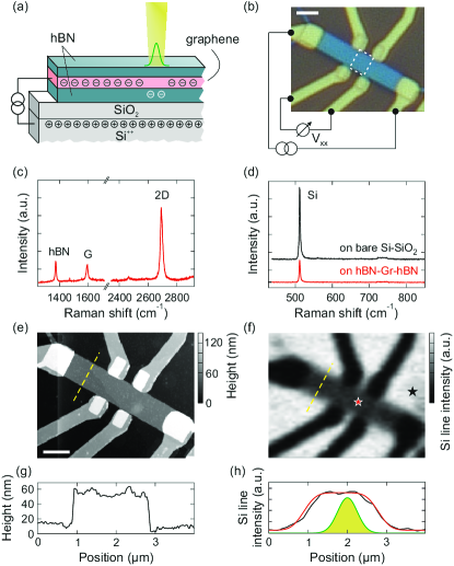
A scanning force microscopy (SFM) image of the Hall bar is shown in Figure 1e. Comparison with a scanning Raman microscopy image (Figure 1f), showing the intensity of the prominent Si Raman line at 520 cm-1 (see spectra in Figure 1d), reveals the high spatial resolution of our optical setup. The silicon peak intensity is reduced when the substrate is covered by the hBN-Gr heterostructure (compare the red and black curves in Figure 1d) and is completely suppressed in metal-coated areas (i.e. on the gold electrodes). Imaging the Si peak intensity allows us to precisely navigate across the device, which is needed for the subsequent experiments. By comparing line cuts of the SFM and scanning Raman microscopy images across the Hall bar (compare Figures 1g and 1h), we can further gain a quantitative measure for the laser spot size. Assuming a Gaussian laser profile and convoluting it with a step function, we adjust the width of the Gaussian so that the convoluted profile matches the Raman line cut (see Figure 1h). This way, we estimate the standard deviation of the Gaussian to be around 250 nm (green curve in Figure 1h), which corresponds to a FWHM of nm. This value sets the size of our laser spot and limits the spatial resolution of the doping profiles discussed below.
The combination of an electrically contacted device with a confocal laser setup allows us to investigate the spatial control of the laser-induced doping profiles in Gr-hBN heterostructures. Ju and coworkers 18 attributed the photo-induced doping effect in hBN-Gr structures to nitrogen vacancies and carbon defects in the hBN, which give rise to defect states deep in the band gap with energies of 2.8 eV (nitrogen vacancy) and 2.6 eV (carbon impurity) 23. They argue that with the help of photons, these states can be occupied by charge carriers injected from the gated graphene18. When the laser is turned on, charge carriers occupying defect states in the hBN layer are excited and, due to the applied gate voltage, move toward the graphene sheet, leaving behind oppositely charged states in the hBN layer. This process continues until the back gate is fully screened by the increasingly charged hBN layer (see also Figure 1a). When turning the laser off again, this effect has effectively shifted the charge neutrality point (CNP) of the graphene sheet to the chosen value of the back gate voltage. Our laser energy of 2.33 eV in combination with the rather high laser intensity (2 to 4 mW) leads to high doping rates, such that only short illumination times are required to shift the CNP.
We expect that the strong photo-induced doping effect in hBN-Gr stacks on SiO2 is closely related to the asymmetric gate oxide structure, i.e. the presence of the insulating SiO2 layer underneath the hBN. The charges injected in the hBN likely diffuse to the bottom of the hBN layer in the direction of the electric field from the Si++ back gate until they are stopped at the SiO2/hBN interface. However, further investigations on the physical mechanisms of the photo-induced doping effect require different sample geometries and spectroscopy analysis techniques, which are beyond the scope of this manuscript. In this work, we focus on the creation, the erasing, the rewriting, and most importantly the spatial resolution of laser-induced doping profiles in this material stack, which do not rely on the use of photo-resists or masks.
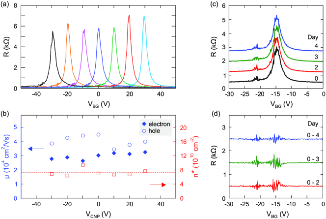
In Figure 2a we show that this effect can be employed to shift the CNP to arbitrary negative as well as positive back gate voltages. To set the CNP of the entire graphene Hall bar to a specific value, we apply the corresponding back gate voltage and scan over the full area depicted in Figure 1f with a total illumination time of 120 s. The typical back gate characteristic of graphene 24 is maintained in all cases. From each back gate characteristic, we extract the electron mobility , the hole mobility , and the charge carrier density fluctuation . The latter has been extracted by the method described in Reference 16 and is a good measure for the electronic disorder (i.e. electron-hole puddles) in bulk graphene. We find average values of cm2/(Vs), cm2/(Vs), and cm-2 (see Figure 2b). Importantly, , , and remain mostly constant for each chosen CNP, which shows the non-destructive nature of this process (Figure 2b). After turning the laser off, the back gate characteristic at 4.2 K remains unchanged for at least four days, which is the longest we have waited without manipulating the doping profile of the sample (see Figures 2c and d).
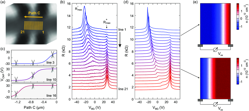
After demonstrating that we can shift the CNP of the entire Hall bar, we next focus on defining spatially varying doping patterns within the graphene sheet. This aspect is highly interesting for potential applications as it enables the definition of re-writable, in-plane p-n and n-p-n junctions with any desired pattern, size, and orientation. To examine the spatial precision of our approach, we start by continuously moving the CNP in the sensitive four-probe area from -30 V to +30 V. In the beginning, the CNP of the entire sample is set to -30 V by scanning over the sample with our laser. Simultaneously, we record a Raman image of the prominent Si line. The integrated Si line intensity is displayed in Figure 3a. In the following, the laser is turned off and the back gate voltage is set to +30 V. Afterward, the laser is turned on for writing a single line across the Hall bar on the very right side of the four-probe area (see vertical line 1 in Figure 3a). The total illumination time during the writing of the line was 7 s. After switching the laser off again, the back gate characteristic of the device is probed, resulting in the upper curve in Figure 3b. This procedure is repeated 20 times. In every iteration, the written line is intentionally shifted by 70 nm to the left (vertical arrow and “Path C” in Figure 3a). The resistance curves obtained after each iteration are displayed in Figure 3b, with the lines offset for clarity. With each line, the CNP of a greater part of the sensitive area is set to +30 V, resulting in the appearance of a typical graphene p-n junction back gate characteristic 25 (middle part of Figure 3b). Additionally, stray light from the laser leads to a continuous doping of the Hall bar and as a result the initial Dirac peak is gradually broadened and shifted toward positive voltages. This effect is especially strong after writing the first line, when the initial Dirac peak is not anymore at -30 V but is shifted to -23 V. Finally, after the entire four-probe area was covered with lines written by the laser, the initial, left Dirac peak has completely vanished and only the new CNP at +30 V can be seen in the back gate characteristic (line 21 in Figure 3b). The steady and continuous shift from an entirely electron-doped four-probe area over a p-n junction to an entirely hole-doped area (see evolution from top to bottom panel in Figure 3c) demonstrates the high spatial precision with which doping profiles can be made with this technique.
To cross-check the measurements, we employ a simple, purely diffusive charge transport model, in which we divide the area where is probed (1.4 µm 1.9 µm; compare white, dashed rectangle in Figure 1b) into individual squares with a size of 10 nm 10 nm each. To each square we then assign a charge distribution
| (1) |
consisting of three contributions. The first contribution, , is the spatially varying doping profile due to the photo-induced doping effect. Each written laser line is modeled as a Gaussian with a standard deviation of 300 nm, which slightly differs from the experimentally determined value (250 nm, see Figure 1h) to account for various experimental uncertainties as described below. Additionally, we add a constant offset to incorporate the initial homogeneous photo-induced doping of the sample. We adjust this constant offset for each trace to account for the increasing stray light-induced doping of the sample. The second contribution, , accounts for the field-effect-induced charge carrier density during a back gate sweep, with V-1cm-2 being the capacitive coupling constant of the back gate as extracted from quantum Hall measurements (not shown). The final contribution, , represents the built-in charge density variations across the sample. In our model, we implement it by assigning a randomly generated number uniformly distributed between and to each square. Finally, we compute the conductivity of every square by
| (2) |
where is the elementary charge, the charge carrier density of the square and is a residual conductivity to account for the finite resistance of graphene at the charge neutrality point adjusted to S to reproduce the data. Furthermore, is the electron/hole mobility, depending on the sign of , for which we use the average values of cm-2/(Vs) and cm-2/(Vs), as obtained from the six back gate traces in Figure 2a. By applying Ohm’s law to each square and relating the currents and voltages of each square via Kirchhoff’s laws, we calculate the total resistance of the graphene sheet from the applied bias voltage and the total outgoing current.
We end up with the simulated back gate characteristics shown in Figure 3d, which match the experimental results quite well. In Figure 3e the corresponding doping profiles of across the four-probe area for two exemplary back gate traces are visualized. The fact that our simple model is able to reproduce the most prominent features of our measurements clearly indicates that the photo-induced doping effect can indeed be effectively used to define spatially resolved doping patterns.
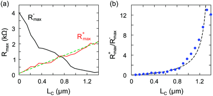
In Figure 4a, we show the maximum resistance value measured at around +30 V back gate voltage (red trace) as well as the maximum value obtained for negative back gate voltage (black trace) as highlighted in Figure 3b. Both peak resistances are plotted against , which is defined as the absolute value of the position of the last, exposed line along ”Path C" prior to measuring the corresponding back gate trace. We observe that with increasing , increases linearly, while drops. In particular, the linear increase of is in good agreement with simple, diffusive transport considerations, where is completely dominated by the length of the sample area with a Dirac point at +30 V. This area increases linearly with , explaining the dependence of . From a linear fit to the data (see green, dashed line in Figure 4a) we extract a resistance change per length of /nm. In Figure 4b the ratio of both resistance peaks is shown (blue points). The continuous increase can be understood from simple diffusive transport considerations. In this case, the ratio of the resistance peaks is given by , where µm. This value highlights the very high sensitivity in resistance change as function of exposed area (i.e. length), which might be of interest for future applications. This expression describes the resistance ratio without any free parameters. The corresponding curve is shown in Figure 4b (dashed, black line). It shows excellent agreement with our measurements. From this representation it is evident that we continuously change the doping profile along ”Path C" upon writing individual lines with a step width of 70 nm and very high spatial precision. Our results show that the resolution of this technique is essentially only limited by the size of the laser spot and the accuracy of sample positioning.
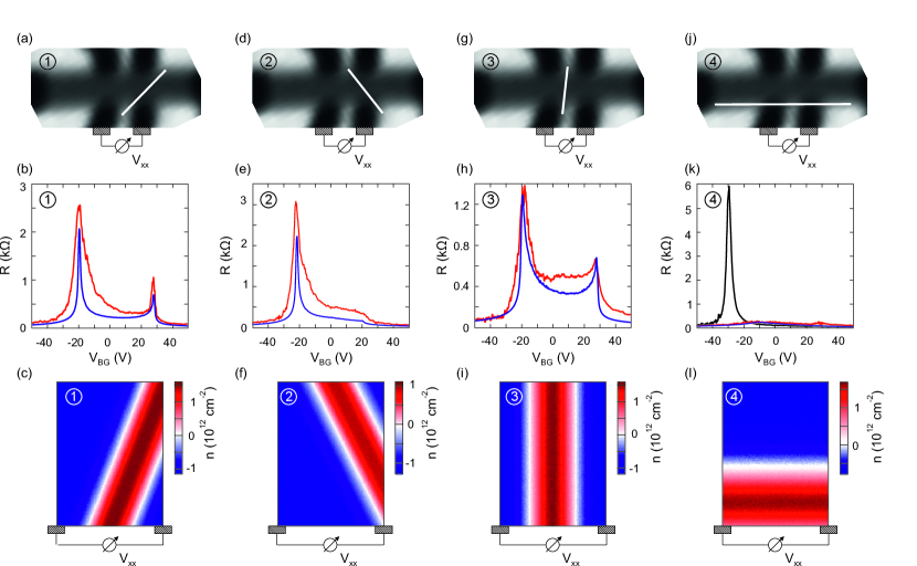
The high spatial precision of the laser-induced doping technique allows the writing and erasing of distinct, well-defined doping profiles. We demonstrate this by writing four different lines with the laser as illustrated in Figures 5a, 5d, 5g, and 5j. In all four cases, the entire sample was first set to a CNP of -30 V before the individual lines were written at a back gate voltage of +30 V. For each case, we cross-check the measurements by using the simple diffusive model described above (and used in Figure 3d) to simulate a similar doping geometry. As before, we adapt the constant doping offset in the simulation to account for stray light from the written lines at +30 V that slightly shifts the -30 V CNP in the rest of the device. We also adjust the width of the simulated Gaussian profile to compensate for uncertainties during the measurement such as a possible misalignment of the optical path and positioning uncertainties due to creeping effects of the piezo stage. Adjusting the width of the Gaussian also partly compensates for the fact that the actual shape of the doping profile induced by a single laser line is not exactly a Gaussian. Once enough charge carriers in the hBN have been excited so that the hBN layer completely screens away the back gate-induced electric field, the photo-doping effect stops and hence the actual doping profile most likely has a saturation area in the center, where the intensity is highest. A good Gaussian profile might only be obtained by perfectly adjusting illumination time and laser intensity to one another.
We start by writing line 1 (see Figure 5a), introducing a p-n junction between the two contacts where is probed. The resulting back gate characteristic is shown in red in Figure 5b, showing the typical p-n junction behavior with two resistance peaks at -20 V and +30 V. It is again evident that stray light plays an important role, as the initial, left CNP is shifted from the original -30 V to -20 V and is also more smeared out than the newly written CNP at positive gate voltage. To confirm the p-n junction doping profile, we calculate the back gate characteristic of a comparable doping pattern (shown in Figure 5c). The resulting trace (blue curve in Figure 5b) reproduces the main features of the measured trace quite well. After erasing the written doping profile and resetting the CNP of the entire Hall bar to -30 V, line 2 is written, again at a back gate voltage of +30 V. As seen in Figure 5d, there is now a conducting path connecting the relevant contacts that is not crossed by the laser line and consequently has its expected CNP at the original -30 V. The measured trace (red line in Figure 5e) indeed shows only one distinct peak at negative gate voltage. This is further backed up by the simulated trace (blue trace in Figure 5e) using the doping profile depicted in Figure 5f. After resetting the CNP of the Hall bar to -30 V, line 3 is written. The measured back gate trace (see red line in Figure 5h) shows two peaks at -20 V and +30 V. Compared to line 1, the peak resistance is significantly lower and the right peak is less distinct, which can be attributed to the above mentioned experimental uncertainties. This is further supported by the calculation (see blue line in Figure 5h), for which the width of the Gaussian profile had to be slightly increased (see Figure 5i). However, from the measurements it is evident that an n-p-n junction can be accurately written with this technique on a length as low as 1.4 µm. Finally, we investigate a fourth interesting doping profile. Again, we first set the entire Hall bar to a CNP of -30 V. The resulting back gate characteristic with a single Dirac peak at -30 V can be seen in Figure 5k (black trace). Afterward, line 4 is written with the laser at +30 V. Since the laser line runs in parallel to the path along which is probed, there is now a highly doped path from source to drain for every value of the back gate voltage, which is reflected in the measured back gate trace, shown in Figure 5k (red curve). As expected, the resistance over the whole range of the back gate voltage is much lower than the resistance measured at the CNP in the homogeneously doped case (black trace). This is further supported by the calculated back gate trace (blue line in Figure 5k) using the doping profile shown in Figure 5l. In all four cases, the qualitative match between the measured and simulated traces indicates that the written laser lines indeed produce the desired doping geometries.
In conclusion, we demonstrated that controllable, laser-induced doping in graphene-hBN heterostructures can be used to define long-term stable doping patterns such as p-n and n-p-n junctions with high spatial resolution and without the use of masks and photo-resists. The CNP of the device can be shifted to any desired value of the back gate voltage without reducing the charge carrier mobility. We focused on the spatial resolution of this technique and demonstrated the continuous evolution of an entirely n-doped graphene regime via a local p-n junction to a fully p-doped regime by step-by-step illumination of small areas of the graphene Hall bar with a green laser. Cross-checking the data with a simple, fully diffusive transport model further underlines that our technique is in principle only limited by the laser spot size (Gaussian standard deviation of 250 nm) and the accuracy of the piezo stage, making it comparable to conventional optical lithography techniques. Consequently, we wrote and erased different doping pattern geometries in a single Hall bar device, creating e.g. a custom-made n-p-n junction. This optical approach to locally dope high-quality graphene devices has distinct advantages over conventional techniques that make use of local gate electrodes in terms of rewritability and a reduction of the amount of difficult and possibly invasive lithography, etching, and contacting steps 9, 10. Additionally, doping patterns with numerous p-n junctions could be implemented and erased in a single device, opening unprecedented opportunities to study graphene-based electron optic devices 26, 27, 28, Veselago lenses 29, and Klein tunneling phenomena30. Moreover, other complex doping profiles which are difficult or impossible to realize with conventional gate electrodes, like isolated, localized doping spots and arrays, can be realized with this technique. Likely, the photo-induced doping effect can be extended to other van der Waals heterostructures based on hBN, opening a wide range of possible studies on the creation of lateral transition-metal-dichalcogenide-hBN transistors without local gate electrodes.
The authors thank M. Drögeler and F. Hassler for helpful discussions. Support by the Helmholtz Nanoelectronic Facility (HNF), the Deutsche Forschungsgemeinschaft, the ERC (GA-Nr. 280140), and the EU project Graphene Flagship (contract no. NECT-ICT-604391), are gratefully acknowledged. S. R. acknowledges funding by the National Research Fund (FNR) Luxembourg.
References
- Ponomarenko et al. 2013 Ponomarenko, L. et al. Nature 2013, 497, 594–597
- Dean et al. 2013 Dean, C.; Wang, L.; Maher, P.; Forsythe, C.; Ghahari, F.; Gao, Y.; Katoch, J.; Ishigami, M.; Moon, P.; Koshino, M.; Taniguchi, T.; Watanabe, K.; Shepard, K.; Hone, J.; Kim, P. Nature 2013, 497, 598–602
- Hunt et al. 2013 Hunt, B.; Sanchez-Yamagishi, J.; Young, A.; Yankowitz, M.; LeRoy, B. J.; Watanabe, K.; Taniguchi, T.; Moon, P.; Koshino, M.; Jarillo-Herrero, P.; Ashoori, R. Science 2013, 340, 1427–1430
- Woods et al. 2014 Woods, C. et al. Nature Physics 2014, 10, 451–456
- Britnell et al. 2013 Britnell, L.; Ribeiro, R.; Eckmann, A.; Jalil, R.; Belle, B.; Mishchenko, A.; Kim, Y.-J.; Gorbachev, R.; Georgiou, T.; Morozov, S.; Grigorenko, A.; Geim, A.; Casiraghi, C.; Castro Neto, A.; Novoselov, K. Science 2013, 340, 1311–1314
- Withers et al. 2015 Withers, F.; Del Pozo-Zamudio, O.; Mishchenko, A.; Rooney, A.; Gholinia, A.; Watanabe, K.; Taniguchi, T.; Haigh, S.; Geim, A.; Tartakovskii, A.; Novoselov, K. Nature Materials 2015, 14, 301–306
- Lu et al. 2014 Lu, C.-P.; Li, G.; Watanabe, K.; Taniguchi, T.; Andrei, E. Y. Physical Review Letters 2014, 113, 156804
- Decker et al. 2011 Decker, R.; Wang, Y.; Brar, V. W.; Regan, W.; Tsai, H.-Z.; Wu, Q.; Gannett, W.; Zettl, A.; Crommie, M. F. Nano Letters 2011, 11, 2291–2295
- Wang et al. 2013 Wang, L.; Meric, I.; Huang, P.; Gao, Q.; Gao, Y.; Tran, H.; Taniguchi, T.; Watanabe, K.; Campos, L.; Muller, D.; Guo, J.; Kim, P.; Hone, J.; Shepard, K.; Dean, C. Science 2013, 342, 614–617
- Engels et al. 2014 Engels, S.; Terrés, B.; Klein, F.; Reichardt, S.; Goldsche, M.; Kuhlen, S.; Watanabe, K.; Taniguchi, T.; Stampfer, C. Physica Status Solidi (b) 2014, 251, 2545–2550
- Engels et al. 2014 Engels, S.; Terrés, B.; Epping, A.; Khodkov, T.; Watanabe, K.; Taniguchi, T.; Beschoten, B.; Stampfer, C. Physical Review Letters 2014, 113, 126801
- Neumann et al. 2015 Neumann, C.; Reichardt, S.; Drögeler, M.; Terrés, B.; Watanabe, K.; Taniguchi, T.; Beschoten, B.; Rotkin, S. V.; Stampfer, C. Nano Letters 2015, 15, 1547–1552
- Kretinin et al. 2014 Kretinin, A. et al. Nano Letters 2014, 14, 3270–3276
- Dean et al. 2010 Dean, C.; Young, A.; Meric, I.; Lee, C.; Wang, L.; Sorgenfrei, S.; Watanabe, K.; Taniguchi, T.; Kim, P.; Shepard, K.; Hone, J. Nature Nanotechnology 2010, 5, 722–726
- Britnell et al. 2012 Britnell, L.; Gorbachev, R.; Jalil, R.; Belle, B.; Schedin, F.; Mishchenko, A.; Georgiou, T.; Katsnelson, M.; Eaves, L.; Morozov, S.; Peres, N.; Leist, J.; Geim, A.; Novoselov, K.; Ponomarenko, L. Science 2012, 335, 947–950
- Couto et al. 2014 Couto, N. J.; Costanzo, D.; Engels, S.; Ki, D.-K.; Watanabe, K.; Taniguchi, T.; Stampfer, C.; Guinea, F.; Morpurgo, A. F. Physical Review X 2014, 4, 041019
- Drögeler et al. 2014 Drögeler, M.; Volmer, F.; Wolter, M.; Terrés, B.; Watanabe, K.; Taniguchi, T.; Güntherodt, G.; Stampfer, C.; Beschoten, B. Nano Letters 2014, 14, 6050–6055
- Ju et al. 2014 Ju, L.; Velasco Jr, J.; Huang, E.; Kahn, S.; Nosiglia, C.; Tsai, H.-Z.; Yang, W.; Taniguchi, T.; Watanabe, K.; Zhang, Y.; Zhang, G.; Crommie, G.; Zettl, A.; Wang, F. Nature Nanotechnology 2014, 9, 348–352
- Kim et al. 2013 Kim, Y. D.; Bae, M.-H.; Seo, J.-T.; Kim, Y. S.; Kim, H.; Lee, J. H.; Ahn, J. R.; Lee, S. W.; Chun, S.-H.; Park, Y. D. ACS Nano 2013, 7, 5850–5857
- Tiberj et al. 2013 Tiberj, A.; Rubio-Roy, M.; Paillet, M.; Huntzinger, J.-R.; Landois, P.; Mikolasek, M.; Contreras, S.; Sauvajol, J.-L.; Dujardin, E.; Zahab, A.-A. Scientific Reports 2013, 3, 2355
- Banszerus et al. 2015 Banszerus, L.; Schmitz, M.; Engels, S.; Dauber, J.; Oellers, M.; Haupt, F.; Watanabe, K.; Taniguchi, T.; Beschoten, B.; Stampfer, C. Science Advances 2015, 1, e1500222
- Neumann et al. 2015 Neumann, C.; Reichardt, S.; Venezuela, P.; Drögeler, M.; Banszerus, L.; Schmitz, M.; Watanabe, K.; Taniguchi, T.; Mauri, F.; Beschoten, B.; Rotkin, S. V.; Stampfer, C. Nature Communications 2015, 6, 8429
- Attaccalite et al. 2011 Attaccalite, C.; Bockstedte, M.; Marini, A.; Rubio, A.; Wirtz, L. Physical Review B 2011, 83, 144115
- Novoselov et al. 2004 Novoselov, K. S.; Geim, A. K.; Morozov, S.; Jiang, D.; Zhang, Y.; Dubonos, S.; Grigorieva, I.; Firsov, A. Science 2004, 306, 666–669
- Williams et al. 2007 Williams, J.; DiCarlo, L.; Marcus, C. Science 2007, 317, 638–641
- Rickhaus et al. 2013 Rickhaus, P.; Maurand, R.; Liu, M.-H.; Weiss, M.; Richter, K.; Schönenberger, C. Nature Communications 2013, 4, 2342
- Young and Kim 2009 Young, A. F.; Kim, P. Nature Physics 2009, 5, 222–226
- Taychatanapat et al. 2015 Taychatanapat, T.; Tan, J. Y.; Yeo, Y.; Watanabe, K.; Taniguchi, T.; Özyilmaz, B. Nature Communications 2015, 6, 6093
- Cheianov et al. 2007 Cheianov, V. V.; Fal’ko, V.; Altshuler, B. Science 2007, 315, 1252–1255
- Beenakker 2008 Beenakker, C. Reviews of Modern Physics 2008, 80, 1337