Current address: ]Aerodyne Research Inc., Billerica, MA Current address: ]IBM T. J. Watson Research Center, Yorktown Heights, NY
Imaging and addressing of individual fermionic atoms in an optical lattice
Abstract
We demonstrate fluorescence microscopy of individual fermionic potassium atoms in a 527-nm-period optical lattice. Using electromagnetically induced transparency (EIT) cooling on the 770.1-nm D1 transition of 40K, we find that atoms remain at individual sites of a 0.3-mK-deep lattice, with a pinning lifetime of , while scattering photons per second. The plane to be imaged is isolated using microwave spectroscopy in a magnetic field gradient, and can be chosen at any depth within the three-dimensional lattice. With a similar protocol, we also demonstrate patterned selection within a single lattice plane. High resolution images are acquired using a microscope objective with 0.8 numerical aperture, from which we determine the occupation of lattice sites in the imaging plane with 94(2)% fidelity per atom. Imaging with single-atom sensitivity and addressing with single-site accuracy are key steps towards the search for unconventional superfluidity of fermions in optical lattices, the initialization and characterization of transport and non-equilibrium dynamics, and the observation of magnetic domains.
Ultracold fermionic atoms in an optical lattice realize an impurity-free analog of electrons in crystalline materials, with full control of parameters such as interaction strength, dimensionality, and tunneling Jaksch and Zoller (2005); Lewenstein et al. (2007). Furthermore, ultracold systems can study many-body physics in scenarios currently inaccessible to materials, such as gauge fields equivalent to thousands of Tesla Gerbier and Dalibard (2010); Aidelsburger et al. (2013); Miyake et al. (2013), interactions at the unitary limit Zwerger (2012), and quantum many-body physics far from equilibrium Lamacraft and Moore (2012). With sufficient control and probes, these experiments can be considered analog quantum simulations Bloch et al. (2012); Georgescu et al. (2014). However, two important tools have been lacking: imaging and addressing fermionic atoms at the single-site and single-atom level Georgescu et al. (2014). When applied to bosonic atoms, these tools have already been dramatically successful Nelson et al. (2007); Gemelke et al. (2009); Bakr et al. (2009); Sherson et al. (2010); Bakr et al. (2010); Weitenberg et al. (2011); Fukuhara et al. (2013); Santra and Ott (2015); Miranda et al. (2015); Islam et al. ; Yamamoto et al. .
High-resolution imaging and manipulation of ultracold fermions solves several outstanding problems at once. First, in-situ spatial probes directly reveal the order parameter of insulating phases, magnetic domain formation, and other correlations inaccessible in time-of-flight imaging Sherson et al. (2010); Bakr et al. (2010); Islam et al. . Second, an ensemble of density distributions provides a direct measure of entropy Sherson et al. (2010); Bakr et al. (2010), extending thermometry of lattice fermions McKay and DeMarco (2011). Third, manipulation of atoms with single-site precision can initiate dynamics Weitenberg et al. (2011); Fukuhara et al. (2013), project or remove disorder Bakr et al. (2010), and selectively remove high entropy atoms to perform in-situ cooling Ho and Zhou (2009); Bernier et al. (2009).
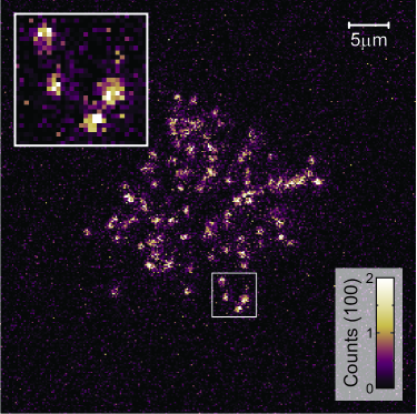
This year, five research groups have succeeded in imaging single fermions in an optical lattice: three using Raman sideband cooling Cheuk et al. (2015); Parsons et al. (2015); Blo and two using EIT cooling Haller et al. (2015), including the results reported in this Article. Our approach is distinguished by a unique imaging configuration, and takes a further step by implementing three-dimensional spatial addressing, which is used here for selective removal of atoms from the lattice. Figure 1 illustrates these abilities with a high-resolution image of 40K atoms sparsely filling a selected 40-site 40-site 1-site volume.
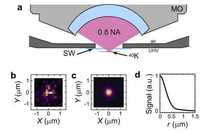
At the heart of our apparatus is a microscope objective with a numerical aperture (NA) of 0.8, placed outside of an ultra-high vacuum (UHV) chamber, 2.0 mm above a 200-m-thick sapphire window [see Fig. 2(a)]. The focal plane of the imaging system is located inside the vacuum, 0.8 mm beyond the thin window. Sapphire is sufficiently hard that this thin substrate can sustain atmospheric pressure with a clear aperture of 5 mm. At the same time, it contributes less spherical aberration than a standard millimeter-thick viewport, since spherical aberration scales as the cube of thickness. The effective point spread function (PSF) of the full imaging system is shown in Fig. 2(c,d) as the average over images of 200 isolated single atoms, centered to sub-pixel precision. Its full width at half maximum (FWHM) of 0.60(1) m is larger than the diffraction limit of 0.5 m, yet small enough to reconstruct the lattice occupation.
Production of ultracold samples begins with the laser cooling and trapping of fermionic 40K and bosonic 87Rb atoms in a glass cell, followed by their transport to a titanium chamber through a succession of magnetic traps. After evaporative and sympathetic cooling to 7 K in a large-volume plugged quadrupole trap, both species are loaded into a crossed optical dipole trap at the focal point of the microscope objective. Further evaporation in the optical dipole trap typically results in degenerate Fermi gases of 40K atoms at . After removal of the 87Rb atoms, this sample is loaded non-adiabatically into a three-dimensional (3D) simple cubic optical lattice, giving a sparse occupation of lattice sites. Each crystal axis is formed by a laser beam at nm: two horizontal beams are retro-reflected in a standard way using mirrors outside of the vacuum system, and the vertical beam is retro-reflected from the sapphire window, which is coated to provide high reflectance at . To prevent interference between axes, the beams are cross-polarized and have a relative frequency detuning. The resulting potential is a separable sinusoid of period . For depths on the order of 10 (where nK and is the atomic mass and is the Boltzmann constant), such a lattice can be used to explore the physics of fermions in the Hubbard regime Bloch et al. (2012); Georgescu et al. (2014). A much deeper () lattice is used during site-resolved imaging to pin each atom to a single site, with typical harmonic trapping frequencies along the lattice axes of kHz.
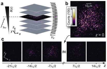
In order to provide well resolved images of atoms in the optical lattice, unobscured by the fluorescence of atoms located outside of the focal plane of the objective, a single plane of the lattice is isolated prior to imaging. With atoms pinned in the lattice, the desired sites are selected by internal state manipulation in the presence of a magnetic field gradient [see Fig. 3(a)] Karski et al. (2010). The gradient is created by quadrupole coils whose axis of symmetry is along . To select atoms in the focal plane of the microscope objective, we apply a G field along , and an amplitude-shaped microwave pulse is swept around the resonance frequency of the target lattice plane. This changes the internal state of the atoms with 95% fidelity, currently limited by our Rabi frequency. Spurious spin-flips in the neighboring planes, away, is fully suppressed. After state manipulation, unwanted atoms are removed from the lattice with a 10-ms-long resonant light pulse which has no effect on the transferred atoms. Finally, the selected atoms are returned to the original internal state. After performing this sequence of microwave and optical pulses a second time, % of the unwanted atoms have been removed while % of the desired atoms are preserved.
Patterning along and is also possible with this protocol, if the applied bias field is oriented along or . For example, Fig. 1 shows the a square pattern selected from the middle of a single lattice plane. This pattern is used for all analyses described below to reduce the effects of lattice inhomogeneity. In-plane patterning has also been demonstrated using projected optical potentials Bakr et al. (2010); Zimmermann et al. (2011); Weitenberg et al. (2011).
Site-resolved reconstruction of single atoms requires that each atom remains pinned in the lattice while scattering photons. Although direct absorption imaging with short light pulses has been demonstrated for Yb Miranda et al. (2015), it is not viable for sub-micron single-atom microscopy of alkali atoms. Instead, light scattering must be accompanied with laser cooling. Since red-detuned D2 molasses Nelson et al. (2007); Bakr et al. (2009); Sherson et al. (2010) is compromised in 40K due to the inverted hyperfine structure of the excited state, we explored in-situ cooling on the (D1) transition at 770.1 nm in 40K. Unlike for D1 cooling in free space Rio Fernandes et al. (2012); Grier et al. (2013); Nath et al. (2013) or in weak traps Salomon et al. (2013); Burchianti et al. (2014) where a Sisyphus mechanism creates a grey molasses Grynberg and Courtois (1994); *Weidemuller:1994vz; *Boiron:1995tt, we observe that a polarization gradient is not essential for cooling in a deep lattice. Instead, dark-state coherence establishes an EIT window that suppresses carrier scattering, while creating an absorption resonance at the red trap sideband, thereby cooling the tightly bound atoms Morigi et al. (2000); *Morigi:2003cv; *Roos:2000ch; *Mucke:2010gh; Haller et al. (2015). Multicolor Raman sideband cooling realizes a similar mechanism Vuletic et al. (1998); Han et al. (2000); Patil et al. (2014), and has also been used for the site-resolved imaging of fermionic atoms Parsons et al. (2015); Cheuk et al. (2015).
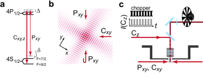
Figure 4 describes our implementation of EIT cooling. Two “coupling” beams (Cxy and Cz) are near the transition, while a weaker “probe” beam (Pxy) is near the transition with differential detuning of from the Raman resonance across ground states. The common-mode detuning from the state of all beams depends on the depth of the optical lattice due to the Stark shift, with larger lattice depth corresponding to smaller . For atoms in the center of the lattice at the depth used for imaging, the Stark shift of the D1 transition is measured to be MHz, and our cooling beams are detuned by MHz. The beam geometry is shown in Fig. 2(b). The Cz beam has W, Pxy has W and is retroreflected, and Cxy has W, providing Rabi frequencies of MHz, MHz, and MHz respectively. Applying these beams scatters photons from the trapped atoms, while the EIT cooling mechanism prevents the atoms from heating out of the lattice sites. Time-of-flight expansion from a 3D lattice after band mapping shows that the majority of atoms remain in the ground vibrational band during imaging.
In order to detect the light scattered from single atoms, it is crucial to eliminate background light. Stray light from the lattice beams can be filtered spectrally, whereas the D1 light cannot. We reduce background light from the horizontal beams Cxy and Pxy with careful beam shaping and alignment, but background scattered light from the vertical cooling beam Cz is unavoidable. The W of Cz is roughly times more powerful than the 20 aW signal of a single atom, and we find that attenuating the Cz background scattering with polarization optics and spatial filters is insufficient in our setup.
Instead, we find that a pulsed cooling method can reduce background light to the level of a single photon per pixel during a 2.6 s exposure. Our approach is depicted in Fig. 4(c): a chopping wheel blocks all light incident on the camera for 50% of the exposure, and the beam Cz is applied for % of the exposure, during periods for which the camera is fully shielded. When unblocked, the camera collects light scattered by atoms from the Pxy and Cxy beams, which also leads to heating of the uncooled vertical degree of freedom. For sufficiently low scattering rates (discussed below), we observe that long pinning times are still attainable with this pulsed cooling method. The time-averaged fluorescence signal is however halved, unlike in schemes where vertical cooling entails a distinguishable wavelength Haller et al. (2015); Cheuk et al. (2015). Including chopping, a 20% collected solid angle, quantum efficiency of the camera, and additional transmission losses, we estimate a net detection efficiency of 7% for scattered photons. Together with our measured photoelectron signal per atom, this collection efficiency implies that the scattering rate is s-1 during EIT cooling.
Images such as Fig. 1 reveal the binary filling of all lattice sites in the selected region, with the help of additional information about the lattice periodicity and the PSF. From a number of similar images, we determine the orientation and apparent period of the optical lattice through evaluation of the relative positions of more than 2000 isolated atoms. Comparing to the known lattice spacing of yields the magnification of our imaging system (). With the lattice angles and magnification determined, we can reconstruct the lattice occupation from each fluorescence image. We expect the apparent lattice occupation to be parity sensitive due to light-assisted collisions Bakr et al. (2009); Sherson et al. (2010), however, our average filling is atom per site, so that occupancies larger than one are rare. Figure 5(a-d) illustrates the steps taken by our reconstruction algorithm to digitize a raw fluorescence image via sharpening and site-binning.
The fidelity of imaging and reconstruction is assessed by comparing digitized images from two sequential exposures of the same arrangement of atoms. Exposures are separated by the 0.4 s required for camera read-out, during which atoms are still laser-cooled. By counting the number of atoms in the second digitization that either appear at an empty site or disappear from an occupied one, we calculate the fraction of atoms which are pinned, hop to a different site, or are lost completely in the second exposure. Figure 6 shows these measures versus several critical imaging parameters.
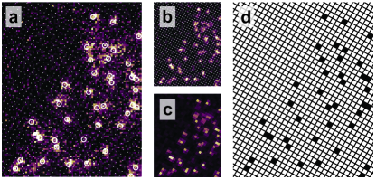
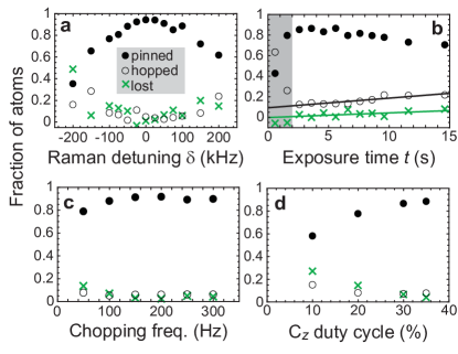
Figure 6(a) shows that optimal cooling is observed for kHz, as was found in prior work Morigi et al. (2000); *Morigi:2003cv; *Roos:2000ch; *Mucke:2010gh; Haller et al. (2015). Here, the dressed ground state is maximally dark to elastic scattering, and inelastic scattering is biased towards red (cooling) transitions. Figure 6(b) shows that long exposures are possible with high fidelity. At short ( s) exposure times, the apparent hopping fraction is high, due to errors in reconstruction with insufficient signal. However at longer exposure times, reconstruction errors are negligible, and loss and hopping approach constant rates of 0.4(3)%s-1 and 1.1(2)%s-1, respectively. This loss rate is consistent with a trap lifetime of 200 s, and a pinned fraction lifetime of 67(9) s.
Figures 6(c,d) evaluate the conditions under which a modulated Cz provides sufficient cooling to the vertical degree of freedom to maintain fidelity. Reducing the chopping frequency below 100 Hz results in a decrease in the fraction of atoms that are pinned to their sites. Fig 6(d) shows that the rate of loss and hopping increases if the duty cycle of Cz is lower than 20%, at a chopping rate of 100 Hz. Thus, a high pinned atom fraction is observed with 3 ms cooling pulses. Combined with the inferred scattering rate, this suggests that approximately six photons can be scattered between vertical cooling cycles.
In optimal conditions, we find that 94(2)% of atoms stay pinned to the same lattice site in a sequence of two images. This is comparable to performance reported in Refs. Parsons et al., 2015; Haller et al., 2015; Cheuk et al., 2015, where pinning fidelity between successive images ranged from 92% to 95%. The fraction of atoms lost in the second image can be as low as 2(1)%. The rest of the 6(2)% of atoms that do not stay pinned either hop or are incorrectly reconstructed in the first or second frame. The optimal exposure time must compromise between signal and hopping during imaging, as shown in Fig. 6(b). This optimum will also depend on lattice filling fraction, since true hopping will become more problematic at high density, where such events will more likely eject a pair of atoms due to light-assisted collisions Nelson et al. (2007); Bakr et al. (2009); Sherson et al. (2010).
In sum, we demonstrate single-atom imaging and selection of fermionic potassium atoms in a far-detuned optical lattice. A crucial realization is that pulsed EIT cooling on the D1 transition of 40K can provide sufficient signal and lifetime for fluorescence microscopy. By reducing background light below the level of a single photon per pixel, the occupation of each lattice site in the imaging plane can be determined with several hundred photons collected per pinned atom. We furthermore demonstrate spectroscopic selection of sites, which has two implications. First, spatially selective removal of atoms is essential to implement the cooling mechanism proposed in Refs. Ho and Zhou, 2009; Bernier et al., 2009. Second, although the microscope can only characterize a single 2D plane, it can be any plane of the 3D optical lattice [see Fig. 3(c)]. This enables the tomographic exploration of 3D physics, which is crucial to model materials such as cuprates, in which “c-axis” tunneling is responsible for long-range order in anti-ferromagnetic and superconducting phases Chakravarty et al. (1988); *Chakravarty:1989he; Kastner et al. (1998); Li et al. (2007); *Berg:2007kn. Even for materials, scanning probes can only measure the surface, while here the imaging plane can be submerged in the bulk. Our results, along with those of Refs. Parsons et al., 2015; Blo, ; Haller et al., 2015; Cheuk et al., 2015, are crucial steps towards the study of strongly correlated phases of fermionic atoms in optical lattices.
Acknowledgements.
We thank S. Heun, C. Kierans, T. Maier, J. McKeever, J. Metzkes, D. Nino, D. Fine, K. Pilch, M. Sprague, J. Sutton, Chen Ge Qu, C. Veit, M. Yee, and Tout Wang for experimental assistance, and M. Greiner, C. Luciuk, D. Weiss, C. Weitenberg, and M. Zwierlein for helpful discussions. This work was supported by AFOSR under FA9550-13-1-0063, by CFI, by the DARPA OLE program, and by NSERC.References
- Jaksch and Zoller (2005) D. Jaksch and P. Zoller, Ann. Phys. 315, 52 (2005).
- Lewenstein et al. (2007) M. Lewenstein, A. Sanpera, V. Ahufinger, B. Damski, A. Sen De, and U. Sen, Adv. Phys. 56, 243 (2007).
- Gerbier and Dalibard (2010) F. Gerbier and J. Dalibard, New J. Phys. 12, 033007 (2010).
- Aidelsburger et al. (2013) M. Aidelsburger, M. Atala, M. Lohse, J. T. Barreiro, B. Paredes, and I. Bloch, Phys. Rev. Lett. 111, 185301 (2013).
- Miyake et al. (2013) H. Miyake, G. A. Siviloglou, C. J. Kennedy, W. C. Burton, and W. Ketterle, Phys. Rev. Lett. 111, 185302 (2013).
- Zwerger (2012) W. Zwerger, ed., The BCS-BEC crossover and the unitary Fermi gas (Springer, Berlin, 2012) and references therein.
- Lamacraft and Moore (2012) A. Lamacraft and J. Moore, in Ultracold Bosonic and Fermionic Gases, edited by K. Levin, S. Fetter, and D. M. Stamper-Kurn (Elsevier, 2012).
- Bloch et al. (2012) I. Bloch, J. Dalibard, and S. Nascimbène, Nature Phys. 8, 267 (2012).
- Georgescu et al. (2014) I. M. Georgescu, S. Ashhab, and F. Nori, Rev. Mod. Phys. 86, 153 (2014).
- Nelson et al. (2007) K. D. Nelson, X. Li, and D. S. Weiss, Nature Phys. 3, 556 (2007).
- Gemelke et al. (2009) N. Gemelke, X. Zhang, C.-L. Hung, and C. Chin, Nature 460, 995 (2009).
- Bakr et al. (2009) W. S. Bakr, J. I. Gillen, A. Peng, S. Foelling, and M. Greiner, Nature 462, 74 (2009).
- Sherson et al. (2010) J. F. Sherson, C. Weitenberg, M. Endres, M. Cheneau, I. Bloch, and S. Kuhr, Nature 467, 68 (2010).
- Bakr et al. (2010) W. S. Bakr, A. Peng, M. E. Tai, R. Ma, J. Simon, J. I. Gillen, S. Foelling, L. Pollet, and M. Greiner, Science 329, 547 (2010).
- Weitenberg et al. (2011) C. Weitenberg, M. Endres, J. Sherson, M. Cheneau, P. Schauß, T. Fukuhara, I. Bloch, and S. Kuhr, Nature 471, 319 (2011).
- Fukuhara et al. (2013) T. Fukuhara, P. Schauß, M. Endres, S. Hild, M. Cheneau, I. Bloch, and C. Gross, Nature 502, 76 (2013).
- Santra and Ott (2015) B. Santra and H. Ott, J. Phys. B 48, 122001 (2015).
- Miranda et al. (2015) M. Miranda, R. Inoue, Y. Okuyama, A. Nakamoto, and M. Kozuma, Phys. Rev. A 91, 063414 (2015).
- (19) R. Islam, R. Ma, P. M. Preiss, M. E. Tai, A. Lukin, M. Rispoli, and M. Greiner, arXiv:1509.01160 .
- (20) R. Yamamoto, J. Kobayashi, T. Kuno, K. Kato, and Y. Takahashi, arXiv:1509.03233 .
- McKay and DeMarco (2011) D. C. McKay and B. DeMarco, Rep. Prog. Phys. 74, 054401 (2011).
- Ho and Zhou (2009) T.-L. Ho and Q. Zhou, Proc. Nat. Acad. Sci. 106, 6916 (2009).
- Bernier et al. (2009) J.-S. Bernier, C. Kollath, A. Georges, L. De Leo, F. Gerbier, C. Salomon, and M. Köhl, Phys. Rev. A 79, 061601 (2009).
- Cheuk et al. (2015) L. W. Cheuk, M. A. Nichols, M. Okan, T. Gersdorf, V. V. Ramasesh, W. S. Bakr, T. Lompe, and M. W. Zwierlein, Phys. Rev. Lett. 114, 193001 (2015).
- Parsons et al. (2015) M. F. Parsons, F. Huber, A. Mazurenko, C. S. Chiu, W. Setiawan, K. Wooley-Brown, S. Blatt, and M. Greiner, Phys. Rev. Lett. 114, 213002 (2015).
- (26) C. Gross and I. Bloch (Private communication).
- Haller et al. (2015) E. Haller, J. Hudson, A. Kelly, D. A. Cotta, B. Peaudecerf, G. D. Bruce, and S. Kuhr, Nature Phys. 11, 738 (2015).
- Karski et al. (2010) M. Karski, L. Förster, J.-M. Choi, A. Steffen, N. Belmechri, W. Alt, D. Meschede, and A. Widera, New J Phys 12, 065027 (2010).
- Zimmermann et al. (2011) B. Zimmermann, T. Müller, J. Meineke, T. Esslinger, and H. Moritz, New J. Phys. 13, 043007 (2011).
- Rio Fernandes et al. (2012) D. Rio Fernandes, F. Sievers, N. Kretzschmar, S. Wu, C. Salomon, and F. Chevy, Europhys. Lett. 100, 63001 (2012).
- Grier et al. (2013) A. T. Grier, I. Ferrier-Barbut, B. S. Rem, M. Delehaye, L. Khaykovich, F. Chevy, and C. Salomon, Phys. Rev. A 87, 063411 (2013).
- Nath et al. (2013) D. Nath, R. K. Easwaran, G. Rajalakshmi, and C. S. Unnikrishnan, Phys. Rev. A 88, 053407 (2013).
- Salomon et al. (2013) G. Salomon, L. Fouché, P. Wang, A. Aspect, P. Bouyer, and T. Bourdel, Europhys. Lett. 104, 63002 (2013).
- Burchianti et al. (2014) A. Burchianti, G. Valtolina, J. A. Seman, E. Pace, M. DePas, M. Inguscio, M. Zaccanti, and G. Roati, Phys. Rev. A 90, 043408 (2014).
- Grynberg and Courtois (1994) G. Grynberg and J. Y. Courtois, Europhys. Lett. 27, 41 (1994).
- Weidemuller et al. (1994) M. Weidemuller, T. Esslinger, M. A. Olshanii, A. Hemmerich, and T. W. Hänsch, Europhys. Lett. 27, 109 (1994).
- Boiron et al. (1995) D. Boiron, C. Triche, D. R. Meacher, P. Verkerk, and G. Grynberg, Phys. Rev. A 52, R3425 (1995).
- Morigi et al. (2000) G. Morigi, J. Eschner, and C. H. Keitel, Phys. Rev. Lett. 85, 4458 (2000).
- Morigi (2003) G. Morigi, Phys. Rev. A 67, 033402 (2003).
- Roos et al. (2000) C. F. Roos, D. Leibfried, A. Mundt, F. Schmidt-Kaler, J. Eschner, and R. Blatt, Phys. Rev. Lett. 85, 5547 (2000).
- Mücke et al. (2010) M. Mücke, E. Figueroa, J. Bochmann, C. Hahn, K. Murr, S. Ritter, C. J. Villas-Boas, and G. Rempe, Nature 465, 755 (2010).
- Vuletic et al. (1998) V. Vuletic, C. Chin, A. J. Kerman, and S. Chu, Phys. Rev. Lett. 81, 5768 (1998).
- Han et al. (2000) D. J. Han, S. Wolf, S. Oliver, C. McCormick, M. T. DePue, and D. S. Weiss, Phys. Rev. Lett. 85, 724 (2000).
- Patil et al. (2014) Y. S. Patil, S. Chakram, L. M. Aycock, and M. Vengalattore, Phys. Rev. A 90, 033422 (2014).
- Chakravarty et al. (1988) S. Chakravarty, B. I. Halperin, and D. R. Nelson, Phys. Rev. Lett. 60, 1057 (1988).
- Chakravarty et al. (1989) S. Chakravarty, B. I. Halperin, and D. R. Nelson, Phys. Rev. B 39, 2344 (1989).
- Kastner et al. (1998) M. A. Kastner, R. J. Birgeneau, G. Shirane, and Y. Endoh, Rev. Mod. Phys. 70, 897 (1998).
- Li et al. (2007) Q. Li, M. Hücker, G. D. Gu, A. M. Tsvelik, and J. M. Tranquada, Phys. Rev. Lett. 99, 067001 (2007).
- Berg et al. (2007) E. Berg, E. Fradkin, E. A. Kim, S. A. Kivelson, V. Oganesyan, J. M. Tranquada, and S. C. Zhang, Phys. Rev. Lett. 99, 127003 (2007).