Feature-rich electronic excitations in external
fields of 2D silicene
Jhao-Ying Wu1,⋆, Szu-Chao Chen, Godfrey Gumbs2,†, and Ming-Fa Lin1,††
1Department of Physics, National Cheng Kung University, Tainan, Taiwan 701
2Department of Physics and Astronomy, Hunter College at the City University of New York,
695 Park Avenue, New York, New York 10065, USA
Electronic Coulomb excitations in monolayer silicene are investigated by using the Lindhard dielectric function and a newly developed generalized tight-binding model (G-TBM). G-TBM simultaneously contains the atomic interactions, the spin-orbit coupling, the Coulomb interactions, and the various external fields at an arbitrary chemical potential. We exhibit the calculation results of the electrically tunable magnetoplasmons and the strong magnetic field modulation of plasmon behaviors. The two intriguing phenomena are well explained by determining the dominant transition channels in the dielectric function and through understanding the electron behavior under the multiple interactions (intrinsic and external). A further tunability of the plasmon features is demonstrated with the momentum transfer and the Fermi energy. The methodological strategy could be extended to several other 2D materials like germanene and stanene, and might open a pathway to search a better system in nanoplasmonic applications.
: 73.22.Lp, 73.22.Pr
I. INTRODUCTION
Silicon photonics is currently a very active and progressive area of research, as silicon optical circuits have emerged as the replacement technology for copper-based circuits in communication and broadband networks. The demand continues for ever improving communications and computing performance, and this in turn means that photonic circuits are finding ever increasing application areas. This paper provides an important and timely investigation of a ”high-priority topic” in the field, covering a particular aspect of the technology that forms the research area of silicon photonics.
Ever since the epitaxial synthesis in 2010 of silicene [1, 2, 3, 4], a buckled structure in which the silicon atoms are displaced perpendicular to the basal plane, there has been a widespread effort by researchers to gain knowledge of its atomic and electronic properties. As an excellent candidate material, silicene is featured with its strong SOC and an electrically tunable band gap. A key effect due to the electric field is that it can open and close the energy band gap which is a desired functionality for digital electronics applications and is one of several potential applications for silicene as a field-effect transistor operating at room temperature [19, 20]. Studied electronic properties include the quantum spin Hall effect, anomalous hall insulators and single-valley semimetals [8], potential giant magneto-resistance [9], superconductivity [10], topologically protected helical edge states [11, 12] and other exotic field-dependent phenomena.
The collective-Coulomb excitations, dominated by the e-e interactions, are important to understand the behavior of electrons in a material. In an intrinsic monolayer silicene, low-frequency plasmons hardly exist, mainly due to the vanishing density of states at the Fermi level. The lack of low-frequency plasmons may be improved by additional dopants or a gate insertion to increase the free-charge density [Wunsch2006, SH2009], i.e., uplifting or lowering the Fermi level to increase the density of states. Alternatively, the free carriers (with zero Fermi energy) may be generated by increasing the thermally excited electrons and holes in the conduction and valence bands, respectively. The intrinsic band gap in silicene would cause the interplay between the intraband and interband transitions and lead to an undamped plasmon at the low frequency [].
A uniform magnetic field would make cyclotron motion of electrons and form the dispersionless Landau levels (LLs), which may enhance the low density of states largely. Unlike graphene, where the n=0 Landau level is pinned at the zero, the stronger spin-orbit coupling (SOC) in silicene causes the n=0 level to split between /2 ( is the amplitude of the effective SOC). In the presence of an electric field, the single-valley Landau levels are no longer spin degenerate and the spin-down and -up states would construct their separate energy gaps. Therefore, it is interesting to investigate how the external fields change the plasmon behaviors.
The present paper is based on the investigation of magnetoplasmons in silicene with the consideration of an electric field and a tunable chemical potential. The calculation is performed by our developed generalized tight-binding model, which simultaneously incorporates all meaningful interactions, including the atomic interaction, the spin-orbit coupling, the Coulomb interaction, and the interaction between the electron and the external fields. This makes our results reliable in a wide range of chemical potentials, the field strengths, and the excitation frequency. The magnetoplasmons can be categorized into two groups: a propagating and a localized mode. The former is strongly driven by the e-e Coulomb interaction, while the latter is mainly dominated by the interaction between the electron and the magnetic field. The electric field is to induce more localized plasmon modes due to the lift of spin and valley degeneracy, a result associated with the buckling geometry structure. On the other hand, the heightened Fermi level would bring about a long-lived propagating plasmon mode. We pay particular attention to the B-dependent plasmon spectrum and observe rich changes in the plasmon features when crossing a critical field strength . The modulation of the plasmon excitations by externally applied electric and magnetic fields means a possible way to design an active plasmon device in the low-buckled materials.
II. METHODS
Similar to graphene, silicene consists of a honeycomb lattice of silicon atoms with two sublattices made up of A and B sites. The difference is that silicene has a buckled structure, with the two sublattice planes separated by a distance of with (Fig. 1). In the tight-binding approximation, the Hamiltonian for silicene in the presence of SOC is given in Refs. [25, 26]: We have
| (1) |
Here, and are creation and destruction operators for an electron with spin polarization at lattice site , when acting on a chosen wavefunction. The sums are carried out over either nearest-neighbor or next-nearest-neighbor lattice site pairs, as indicated. The first term (I) takes care of nearest-neighbor hopping with transfer energy eV whereas the third term (II) describes the effective SOC for parameter meV and is the vector of Pauli spin matrices. Additionally, we chose if the next-nearest-neighboring hopping is anticlockwise/clockwise with respect to the positive axis. In the third term (III), We include the intrinsic Bychkov-Rashba SOC via meV for the next-nearest neighbor hopping and set for the A/B lattice site, respectively, and with the vector joining two sites and on the same sublattice. The staggered sublattice potential energy produced by the external electric field is described by the fourth term where for the A/B sublattice site and =0.23 .
The monolayer silicene is assumed to be in an ambient uniform magnetic field . The magnetic flux, the product of the field strength and the hexagonal area, is where . The vector potential, which is chosen as , leads to a new periodicity along the armchair direction. The unit cell is thus enlarged and its dimension is determined by . The enlarged unit cell contains 4 Si atoms and the Hamiltonian matrix is 88 including the spin degree. The hopping parameter acquires the extra position-dependent Peierls phase is given by
| (2) |
The phases of the first three terms of the hopping integrals in Eq. (1) associated with the additional position-dependent Peierls phases are given in order:
| (4) | |||||
with and .
| (6) | |||||
where .
| (8) | |||||
and .
| (10) | |||||
In this notation, .
| (12) | |||||
and . Also,
| (14) | |||||
where . We also introduce
| (16) | |||||
with }.
| (18) | |||||
with }. Further, we have
| (20) | |||||
with }. By diagonalizing our Hamiltonian, the eigenenergy and the wave function are derived ( and refer to the conduction and valence bands, respectively).
When a uniform magnetic field is applied to silicene, the electronic states are dispersionless Landau levels (LLs) whose behavior is governed by the energy dispersion in the absence of a magnetic field. Due to the existence of two valleys and spin degrees of freedom, each LL is eight-fold degenerate with successive LL spacing decreasing with increasing energy. The number of nodes of an occupied or unoccupied LL wavefunction is equal to the quantum number ( of each conduction (valence) LL below or above the chemical potential. We note that the LL is four-fold degenerate. Electrons may be excited from valence LLs to conduction LLs in doped silicene through electron energy loss spectroscopy (EELS) or when light is absorbed, for example. However, in addition to single-particle excitations (SPEs) between LLs, there are collective magnetoplasmon modes whose frequencies are depolarization shifted due to the Coulomb interaction and are dispersive functions of the transfer momentum . In our notation, we label each inter-Landau level excitation channel by (, ) and the order of the transition by .
The dispersion relation for the spectrum of collective plasmon modes may be determined from the energy loss function to be evaluated from the imaginary part of the inverse dielectric function where in the random-phase approximation (RPA), we have with the 2D polarization function given by [28, 29]
| (21) |
in terms of the form factor arising from the overlap of the eigenstates. The equilibrium Fermi-Dirac distribution function is , where is Boltzmann’s constant. Additionally, is an energy broadening parameter which may arise from various dephasing mechanisms, and is the chemical potential whose temperature dependence may be neglected over the range we investigated. Also, where is given in terms of the permeability of free space and the background dielectric constant of silicene. Corresponding to each Landau level transition channel, the Re has a symmetric peak when plotted as a function of frequency and a pair of asymmetric peaks. If these peaks occur where vanishes, then they determine the frequencies of undamped magnetoplasmon excitations.
III. RESULTS AND DISCUSSION
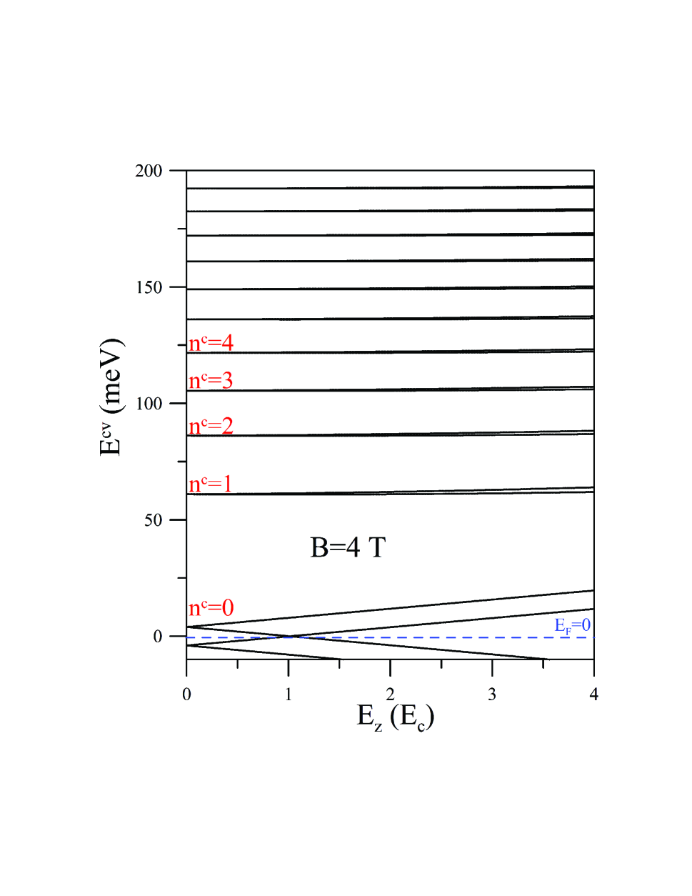
The main difference between the LL spectrum of silicene and that of graphene is the splitting of the LL which is due to the significant SOC. Also, a larger Brillouin zone in silicene means that there is a higher carrier density per LL and a wider energy spacing than graphene for a chosen magnetic field. This could make it easier to observe the integer quantum Hall effect at the ambient condition. Another property of silicene is the double-gap energy band structure under an external electric field , and the transition from topological insulator (TI) to band insulator (BI) when . Such features are illustrated in Fig. 1 for -dependent LL spectrum. Based on the node structure of the Landau wavefunctions, the quantum number () for each conduction (valence) LL could be determined by the number of zeroes; this is the same as the number labeling the th unoccupied (occupied) LL above (below) the Fermi energy =0 []. (The two localization positions correspond to the two valley structures.) A very small band gap (7.9 meV) already exists at . That is, the LL is twice less degenerate than the LLs. A finite splits the LLs and lifts the spin and valley degeneracies for the n=0 LLs. This creates two energy gaps with one of them increasing with and the other decreasing for . The lowest gap is closed at (), meanwhile the difference between the two energy gaps reaches the maximum. After that, both the two gaps are increased with the increment of . The process is a signature of band inversion associated with the transition between the TI to BI regimes. The splitting of LLs is only obvious at larger ( ).
Through the Coulomb interaction, electrons may be excited from the valence to conduction LLs for the intrinsic condition. A single-particle mode has an excitation energy according to the conservation laws of energy and momentum. In the discussion below, we use a pair of numbers (,) to label a LL transition channel. Here, and denote the quantum numbers of the initial and final states, respectively. For example, (,) denotes the transition from the highest occupied LL to the second-lowest unoccupied LL, and has the same excitation energy as (,) because of the inversion symmetry between the conduction and valence LLs. The transition order is denoted as , which is useful to categorize the SPE channels. The number pair is also used to label a plasmon mode, meaning that the plasmon mode is predominantly dominated by the SPE channel. This is seen in the plasmon frequency that approaches the SPE energy in the large or small limit of , as discussed later in Fig. 4.
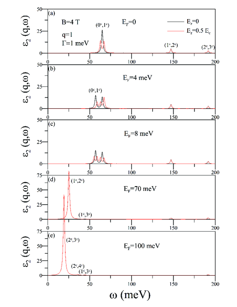
The SPE spectrum is obtained by calculating the imaginary part of the dielectric function (Fig. 2). Each prominent peak in represents a major LL transition channel. Their intensity is determined by the wave function overlap between the initial and final states, as given in the Coulomb-matrix elements , and therefore strongly depends on . A SPE channel with smaller transition order () and quantum numbers has larger value of the Coulomb-matrix elements for a smaller , and the converse is true for a channel with larger transition order and quantum numbers. This is according to the characteristics of the Hermite polynomials. For (in unit of ) and Fermi energy , as shown in Fig. 2(a) by the black curve, the three-lowest frequency peaks are labeled by (,), (,), and (,) from low to high. They represent the interband channels with . The effect of the Fermi level variation is shown in Figs. 2(b)-(e) by the black curves. When lies between the n=0 and 1 LLs (Figs. 2(b) and 2(c)), it causes the interband feature of (,) to decrease in intensity by a factor of two as half the spectral weight is shifted to a low-energy intraband peak (,). When is situated between the n=1 and 2 LLs (Fig. 2(d)), the peaks associated with transitions to and from the n=0 LLs disappear due to Pauli Blocking, and the intraband peak emerges. The lowest intraband channel has a quite lower frequency and a quite stronger intensity than that of the lowest interband channel owing to the reduced LL spacings at higher energies and the in-phase Landau wavefunction transition. Peak is diminished and replaced by the intraband peak as the transitions to the n=1 LL are Pauli blocked ((Fig. 2(e)). With higher , a similar redistribution of spectral weight is observed.
A finite would lift the spin and valley degeneracies of n=0 LLs and enrich the SPE spectrum, as shown by the red curves in Figs. 2(a)-2(e) for . At (Fig. 2(a)), the peak is split into two: the lowest and the second-lowest interband peaks. The movement of the lowest (second-lowest) interband peak to lower (higher) frequency corresponds to the closing (increasing) band gap. The first feature reaches to the lowest frequency () when the band gap completely closes at . For , both two split peaks move to higher energies due to the reopening of the lowest gap. When is above three n=0 levels (Fig. 2(b)), the lowest interband peak redistributes its spectral weight to a lower intraband peak. If is further moved to above all n=0 LLs and below the n=1 LLs (Fig. 2(c)), the second-lowest interband peak redistributes its spectral weight to the lowest intraband peak. Therefore, four robust spin- and valley-polarized peaks are obtained. When is situated above the n=1 LL (Figs. 2(d)) or higher (Figs. 2(e)), the spin- and valley-polarized peaks could be only observed at higher q’s for that the higher transitions from and to the n=0 LLs are allowed.
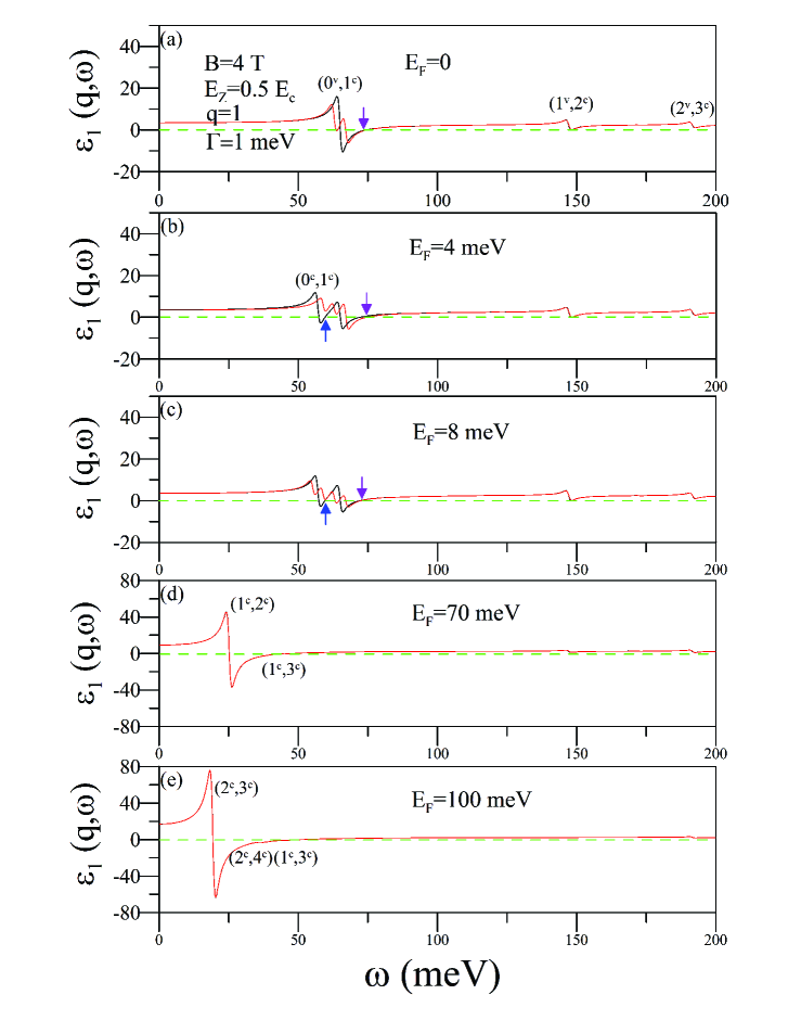
The real parts of dielectric functions are connected with the imaginary parts by the Kramers-Kronig relations (Figs. 3(a)-3(e)). A symmetric peak in corresponds to a pair of asymmetric peaks in . The asymmetric peaks could induce zero points. If the zero point exists where vanishes, then an undapmed plasmon could occur at that frequency. In the case of and below the LL (Figs. 3(a)-3(c)), a zero point induced by the channel is located where other SPE channels are weak (indicated by the purple arrows). Therefore, an undamped plasmon is expected to appear there. Though the intraband peak (,) creates a zero point also (indicated by the blue arrows in Figs. 3(b) and 3(c)), it is located at a finite value of from the adjacent interband channel (,). Consequently, only a strongly damped plasmon could occur there. If is above the LL (Fig. 3(d)), a lower zero point is collectively induced by the intraband channels and . The derivative of with respect to frequency around the zero point is relatively small compared to that created by the interband channel (). Therefore, a plasmon with a lower frequency and a stronger intensity is predicted. For an even higher (Fig. 3(e)), more intraband channels involve the zero point. At a high-limit value of , all the low-frequency transition states may collectively contribute to one zero point, which is similar to a classical dielectric form.
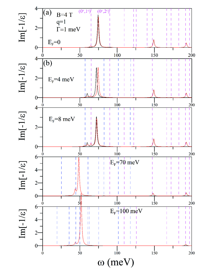
The energy-loss function, defined as , is useful for understanding the collective excitations and the measured excitation spectra, such as in the inelastic light and electron scattering spectroscopies. Each prominent structure in may be viewed as a plasmon excitation with different degrees of Landau damping. For and (the black curve in Fig. 4(a)), the lowest and also the strongest peak is located between the SPE energies of and , where corresponds to a zero point in and a quite small value in . The second and the third peaks, which are close to the SPE energies of and , respectively, are relatively weak due to significant Landau damping.
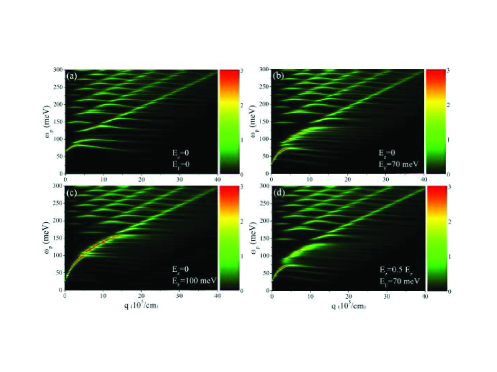
When lies between the n=0 and 1 LLs (Figs. 4(b) and 4(c)), the spectral weight of the first plasmon peak is shifted to a low-energy intraband plasmon. If is between the and 2 levels (Fig. 2(d)), the threshold peak is replaced by a lower intraband plasmon which is contributed by channels and . The intraband plasmon involves more low free-charge carriers and has the stronger intensity than any interband features. For an even higher , the intraband plasmon grows in intensity obviously, a result of the increased (decreased) number of intraband (interband) transition channels plotted in the blue (red) dashed lines in Fig. 4(e). A finite () would lower the threshold-excitation frequency due to the splitting of plasmon peaks () and (), as shown in Figs. 4(a)-4(c) by the red curves. The newly created peaks suffer a quite strong Landau damping since the splitting energies between the n=0 LLs are quite small. The splitting energies may be improved by a stronger , and then the low plasmon peaks are enhanced. This is illustrated by the blue curves in Figs. 4(a)-4(c) for . When is situated above the n=1 LL or higher (Figs. 4(d) and 4(e)), the effect of the E-field is only evident at higher q’s. This is seen in the plasmon dispersion later.
The magnetoplasmon spectrum possesses an intriguing dependence on , as shown in Fig. 5. Each plasmon branch is strongly confined in between the energies of two close SPE channels (illustrated by the two white-dashed lines for the lowest plasmon branch) and exists only in a limited -range. In both the short and long wavelength limits, plasmons are overly damped and have frequencies close to the SPE energies. Therefore, a characteristic behavior of the magnetoplasmons is that in the long wavelength limit their group velocity is positive and the plasmon intensity is increased as is increased. The group velocity becomes zero at a critical momentum where the length scale for density fluctuations is comparable to the cyclotron radius. As for , the group velocity becomes negative and the plasmon intensity is decreased by further increasing . The value of is increased when the magnetic field is increased. For a plasmon-excitation channel, the larger the transition order , a larger rate of increase in as a function of is obtained [ACS NANO 5,1026 (2011)]. The peculiar dependence of on may cause a rich -dependent plasmon spectrum, as demonstrated in later plots.
The dispersion relation of the intraband magnetoplasmons is quite different from the interband ones’. When the LL is occupied (Fig. 5(b)), the lowest interband plasmon branch no longer exists and is replaced by a combination of three intraband modes: , and . The three intraband channels form a continuous branch which exhibits a longer range of positive slope (group velocity) and higher intensity. Besides, the disappearance of the interband plasmon helps to enhance the other interband modes, such as and . Although these interband plasmons are close to each other, they disperse independently, because they experience quite a strong restoring force which comes from the magnetic field. The intraband magnetoplasmon would extend to the higher frequency for a higher Fermi level (Fig. 5(c)) owning to the increased number of intraband channels. Meanwhile, the gap between the intraband plasmon and the lowest interband plasmon is reduced. A finite would induce extra branches mainly out of the splitting of LLs, as shown in Fig. 5(d) for meV and . Those newly created modes (marked by the purple arrows) are weakly dispersive. The locations and the number of the sub-branches vary with the Fermi level. They could be used as a fine tuning of the magnetoplasmon spectrum, like the threshold-excitation frequency, the energy spacings and the density of excitation channels.
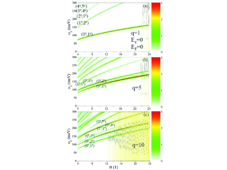
The plasmon spectra at various ’s and ’s have different dependencies on the magnetic field. For and a small q=1, the plasmon modes are dominated by the SPE channels with according to the characteristics of Hermite polynomial functions. The frequencies and intensities of these modes grow monotonically with (Fig. 6(a)), which corresponds to an enhanced carrier density per LL and enlarged LL spacings. When is increased to 5 (Fig. 6(b)), the plasmon modes with become more intense. Such channels have the larger than those of and hardly exist at the long wavelength limit (). This is because the plasmon intensity is reduced when is away from . The critical momentum grows with increased on the account of the increased ratio of the wavelength to the magnetic length. Therefore, if is set to a value less than for a plasmon mode, an increasing in effect causes to deviate from that weakens the plasmon further. This is seen in the branches of and in Fig. 6(b). On the other hand, if is set to a value larger than , an increasing will move closer to the fixed value of . All plasmon modes in such the condition are intensified consistently by an increasing , as shown in Fig. 6(c) for .
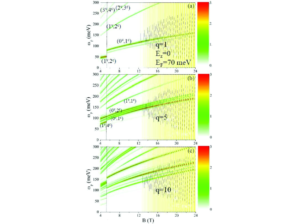
In the condition of that LL is occupied (Fig. 7), the plasmon spectrum experiences an abrupt change in the intensities, frequencies, and bandwidths at the critical field strength T. This is because that above the all electrons may be accommodated in the LLs. For (Fig. 7 (a)), the lowest dominant transition channel is changed from the intraband to the interband at the . In contrast, the other interband channels are increased in intensities and frequencies continuously. At (Fig. 7(b)), the obvious change in the plasmon spectrum after the cross of is the discontinuous transformation from the lowest intraband channel to the lowest interband and the appearance of the interband branch . The distinct -dependent behaviors between the intraband and interband plasmon modes is a vivid feature to distinguish the two kinds of transition channels. At , there are more channels from and to the n=1 LL , like (5,1) and (8,1), as shown in Fig. 7(c). These channels disappear at the and create more discontinuous features. The result demonstrates that the momentum transfer is an important factor to perform a tunable B-dependent plasmon spectrum.
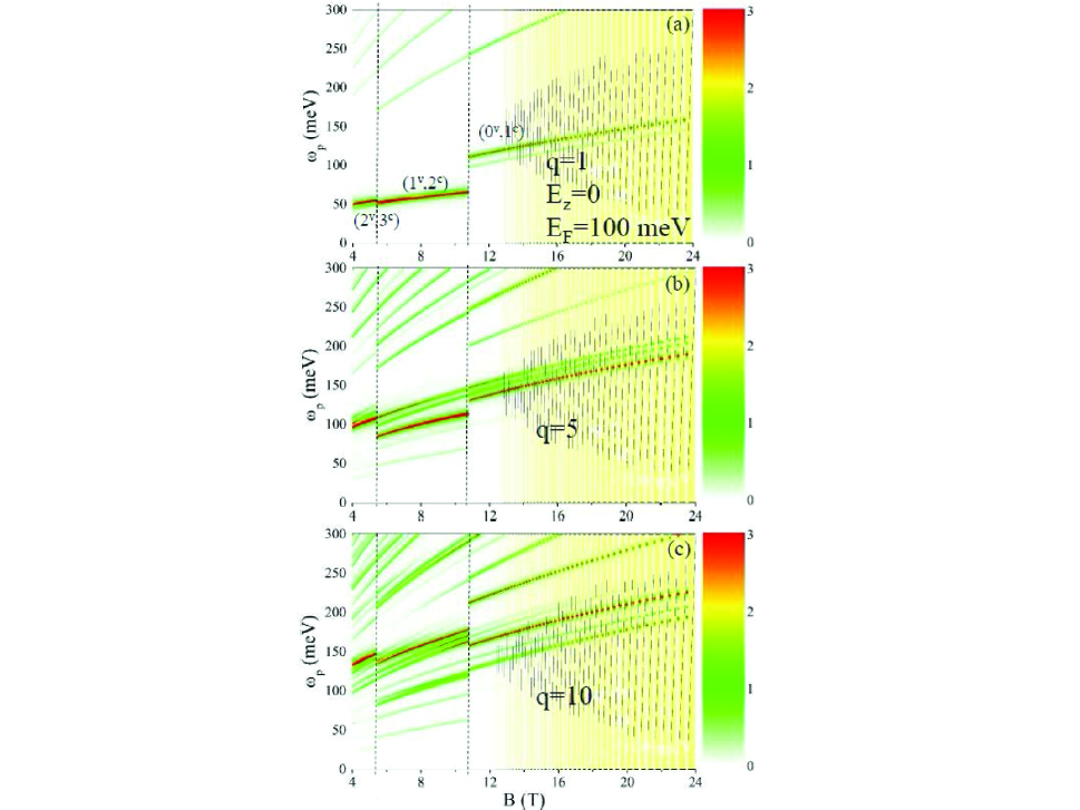
If both the and LLs are occupied, there are two ’s through which (the quantum number of the highest occupied LL) is decreased to , as shown in Fig. 8. The first critical magnetic field is T (the same with that in Fig. 7), and the second is T. For q=1 (Fig. 8(a)), the lowest intraband channel is changed to intraband at , and then the intraband channel () is further changed to interband () at . The conditions of various q’s are displayed in Figs. 8(b) and 8(c). Generally speaking, the plasmon spectrum are distinct in the three field-strength ranges: , , and . The three regions show the features of the LL spectrum with the highest occupied quantum number: n=2, n=1, and n=0, respectively. The discontinuous plasmon behaviors at could be verified experimentally. The novel feature with the strong dependence on wave vector as well as the excitation channels may be useful for the design of magneto-plasmonic components for varied applications.
IV. SUMMARY AND CONCLUSIONS
In summary, the magnetoplasmon behaviors in monolayer silicece are studied by the novel GTBM. GTBM simultaneously includes the atomic interaction, the spin-orbit coupling, the Coulomb interaction, and the effect of external fields. The buckling structure and the significant SOI warrant an electrically tunable energy gap and spin- and valley- polarized LLs in a magnetic field. This reflects in the energy spacing and the number of magnetoplasmon peaks. The extra plasmon branches induced by the E-field have weak dependence on the momentum transfer, which means that the buckling structure and the magnetic field combine to localize them. The heightened Fermi level is shown to redistribute spectral weight from discrete interband transitions to a strong low-energy intraband plasmon. The two plasmon modes differ in the dependence on the momentum and the B-field strength. In particular, discontinuous changes in the plasmon features are found when field strength is equal to . At the crossing of each , the quantum number of the highest occupied LL is changed from to . We demonstrate that the characteristic B-dependent plasmon behaviors are strongly determined by the momentum transfer. This is due to the different of each plasmon branch (plasmon at has zero group velocity). The methodology is suitable to treat a large variety of forms of external fields, including uniform and nonuniform electric and magnetic fields. Also, it can be extended to other nanomaterials at a wide range of chemical potentials. Therefore, this work suggests a guide in searching the materials for better nanoplasmonic applications.
In summary, we have calculated the charge carrier plasmon dispersion relation in silicene under conditions of variable perpendicular electric and magnetic fields as well as the adjustment of free carrier density is adjusted by doping the sample. The non-dispersive Landau level energy bands may be characterized as being in two spin-up and spin-down subgroups due to the presence of spin-orbit coupling. A major effect arising from the applied electric field on the LLs is to lift the degeneracy of the up and down spin states for intrinsic silicene. On the other hand, in the absence of an electric field, doping would create more separated plasmon branches, which involve the two separated LLs. Consequently, the LLs may be split and inter-LL transitions may lead to a novel quasiparticle excitation spectrum which is not possible to achieve without these three contributing factors being applied simultaneously. Most notably, we observed the appearance of a group of dispersionless plasmon excitations which means that the buckling geometry and magnetic field combine to localize them.
Our analysis has demonstrated that the plasmon dispersion of 2D systems can be even more easily tuned than their 3D counterparts when carrier doping, electric and magnetic fields together act. The negative dispersion in the plasmon spectrum can be switched to positive by doping with electrons or holes. Additionally, the plasmon nature is determined by an interplay between the Coulomb interaction and the interband LL transitions, which gives rise to a small bandwidth corresponding to localized plasmons at high doping as shown in Fig. 5. Thus, we have managed to tune the plasmon character microscopically through the charge response to a strong local field in silicene. Therefore, doped silicene in perpendicular electromagnetic fields seem promising for further investigation experimentally.
ACKNOWLEDGMENT
Acknowledgments. This work was supported by the NSC of Taiwan, under Grant No. NSC 102-2112-M-006-007-MY3.
⋆e-mail address: yarst5@gmail.com
†e-mail address: ggumbs@hunter.cuny.edu
††e-mail address: mflin@mail.ncku.edu.tw
References
- [1] .B. Aufray, A. Kara, S. Vizzini, H. Oughaddou, C. Landri, B. Ealet, G. Le Lay, Appl. Phys. Lett. 96, 183102 (2010).
- [2] Patrick Vogt, Paola De Padova, Claudio Quaresima, Jose Avila, Emmanouil Frantzeskakis, Maria Carmen Asensio, Andrea Resta, Bndicte Ealet, and Guy Le Lay, Phys. Rev. Lett. 108, 155501 (2012).
- [3] Lan Chen, Cheng-Cheng Liu, Baojie Feng, Xiaoyue He, Peng Cheng, Zijing Ding, Sheng Meng, Yugui Yao, and Kehui Wu Phys. Rev. Lett. 109, 056804 (2012).
- [4] Z. L. Liu, M. X. Wang, J. P. Xu, J. F. Ge, G. L. Lay, P. Vogt, D. Qian, C. L. Gao, C. Liu, and J. F. Jia New J. Phys. 16, 075006 (2014).
- [5] N. Takagi, Chun-Liang Lin, K. Kawahara, E. Minamitani, N. Tsukahara, M. Kawai, and R. Arafung, Progress in Surface Science 90, 1 (2015).
- [6] H. Oughaddou, H. Enriquez, M. R. Tchalala, H. Yildirim, A. J. Mayne, A. Bendou,nan, G. Dujardin, M. A. Ali, and A. Kara, Progress in Surface Science 90, 46 (2015).
- [7] G. G. Guzman-Verri, L. C. Lew Yan Voon, Phys. Rev. B 76, 075131 (2007).
- [8] C.-C. Liu, W. Feng, Y. Yao, Phys. Rev. Lett. 107, 076802 (2011).
- [9] S. Rachel, M. Ezawa, Phys. Rev. B 89, 195303 (2014).
- [10] F. Liu, C.-C. Liu, K. Wu, F. Yang, and Y. Yao, Phys. Rev. Lett. 111, 066804 (2013). 9.
- [11] M. Ezawa, Phys. Rev. B 87, 155415 (2013).
- [12] Hao-Ran Chang, Jianhui Zhou, Hui Zhang, and Yugui Yao, Phys. Rev. B 89, 201411(R) (2014).
- [13] A. Yamakage, M. Ezawa, Y. Tanaka, N. Nagaosa, Phys. Rev. B 88, 085322 (2013).
- [14] J. Sivek, H. Sahin, B. Partoens, and F. M. Peeters, Phys. Rev. B 87, 085444 (2013).
- [15] A. Kara, H. Enriquez, A.P. Seitsonen, L.C.L.Y. Voon, S. Vizzini, B. Aufray, H. Oughaddou, Surf. Sci. Rep. 67, 1 (2012).
- [16] H. Enriquez, S. Vizzini, A. Kara, B. Lalmi, H. Oughaddou, J. Phys.: Condens. Matter 24, 314211 (2012) .
- [17] B. Lalmi, H. Oughaddou, H. Enriquez, A. Kara, S. Vizzini, B. Ealet, B. Aufray, Appl. Phys. Lett. 97 223109 (2010) .
- [18] M. R. Tchalala, H. Enriquez, A.J. Mayne, A. Kara, G. Dujardin, M. Ait Ali, H. Oughaddou, J. Phys: Conf. Ser. 491, 012002 (2014).
- [19] Li Tao, Eugenio Cinquanta, Daniele Chiappe, Carlo Grazianetti, Marco Fanciulli, Madan Dubey, Alessandro Molle, and Deji Akinwande, Nature Nanotechnology 10, 227 (2015).
- [20] Guy Le Lay, Nature Nanotechnology 10, 202 (2015).
- [21] C. J. Tabert and E. J. Nicol, Phys. Rev. B 88, 085434 (2013).
- [22] C. J. Tabert and E. J. Nicol, Phys. Rev. Lett 110, 197402 (2013).
- [23] C. J. Tabert and E. J. Nicol, Phys. Rev. B 89, 195410 (2014).
- [24] B. Van Duppen, P. Vasilopoulos, and F. M. Peeters, Phys. Rev. B 90, 035142 (2014).
- [25] C. C. Liu, H. Jiang, and Y. Yao, Phys. Rev. B 84, 195430 (2011).
- [26] M. Ezawa, Phys. Rev. Lett. 109, 055502 (2012).
- [27] Jhao-Ying Wu, Chiun-Yan Lin, Godfrey Gumbs, and Ming-Fa Lin, Royal Society of Chemistry Advances 5, 51912-51918 (2015).
- [28] R. Roldn, J.-N. Fuchs, and M. O. Goerbig, Phys. Rev. B 80, 085408 (2009).
- [29] O. L. Berman, G. Gumbs, and Y. E. Lozovik, Phys. Rev. B 78, 085401 (2008).