Quasinormal mode theory and modelling of electron energy loss spectroscopy for plasmonic nanostructures
Abstract
Understanding light-matter interactions using localized surface plasmons (LSPs) is of fundamental interest in classical and quantum plasmonics and has a wide range of applications. In order to understand the spatial properties of LSPs, electron energy loss spectroscopy (EELS) is a common and powerful method of spatially resolving the extreme localized fields that can be obtained with metal resonators. However, modelling EELS for general shaped resonators presents a major challenge in computational electrodynamics, requiring the full photon Green function as a function of two space points and frequency. Here we present an intuitive and computationally simple method for computing EELS maps of plasmonic resonators using a quasinormal mode (QNM) expansion technique. By separating the contribution of the QNM and the bulk material, we give closed-form analytical formulas for the plasmonic QNM contribution to the EELS maps. We exemplify our technique for a split ring resonator, a gold nanorod, and a nanorod dimer structure. The method is accurate, intuitive, and gives orders of magnitude improvements over direct dipole simulations that numerically solve the full 3D Maxwell equations. We also show how the same QNM Green function can be used to obtain the Purcell factor (and projected local density of optical states) from quantum dipole emitters or two level atoms, and we demonstrate how the spectral features differ in general to the EELS spectrum.
I Introduction
Nanoplasmonics continues to receive substantial interest from various fields of research including biology Bio1 ; Bio2 , chemistry Chem1 ; Chem2 and physics Phys , with applications ranging from renewable energy technology Plasmonicsphotovoltaic to homeland security by the sensitive identification of explosive material Secu . Due to the collective excitations of electrons at the surface of a metallic resonator coupling to electromagnetic fields, the local density of optical states (LDOS) decreases rapidly for spatial positions away from the surface of the metal resonator; so-called “hot spots”, where the local electric field can be enhanced by orders of magnitude in comparison to a bulk medium, are formed near the surface. The unique properties of localized surface plasmon (LSP) resonances, manifest in a strong confinement of electric field far below the diffraction limit and result in an exotic electromagnetic response that underlines the wide application of surface plasmons, especially in nanoscience and nanophotonics; however, the extreme spatial localization of LSPs makes them experimentally challenging for direct detection of the spatial field distribution, e.g., by employing conventional spectroscopy techniques, since the spatial resolution is constrained by the diffraction limit. In addition, optically dark modes have a vanishing dipole moment, and traditional optical methods fail to excite such modes.
Due to the strong frequency dispersion and losses in metals, which satisfy the Kramers-Kronig relations, it is a very challenging problem to model the electromagnetic response of arbitrarily shaped metal resonators. Consequently, most optical studies of plasmonic structures rely heavily on brute force numerical simulations. Direct imaging of the LSP resonances is important both for revealing the exotic physics underlying these resonances and for verifying and testing numerical models used in theoretical studies. There are presently several different experimental schemes developed to detect the electromagnetic component of LSPs, including near-field scanning optical microscopy (NSOM) NSOM ; NSOM1 , leakage radiation microscopy LMS , and two-photon induced photoluminescence NTPL ; TPL , and cathodoluminescence Los . Of particular interest, electron energy loss spectroscopy (EELS) has been shown to be capable of accessing the subwavelength spatial variation of the surface plasmon modes of single metallic nanoresonator experimentally Nelayah ; Bosman for almost a decade; during this time, it has been recognized to be EELStheo ; EELStheo2 ; EELSr one of the most powerful approaches, in which high speed electron beams (typically ranging from several tens to several hundreds of keV) are injected and transmitted across an optically thin sample, with a spatial resolution of around 1 nm; EELS has been applied to various systems such as split ring resonator (SRR) Husnik and single nanorod/antennas Nico ; Ross . The EELS method is also quite versatile, allowing one to probe both optically bright and dark resonances over broadband frequencies, and can be used for detecting both localized and extended excitations EELSr . Recently, vortex electron beams have also been experimentally demonstrated Vortexelectron ; Vortexe2 , which may find use for probing the magnetic component of LSPs VEELSGordon .
Modelling EELS is an extremely challenging and tedious numerical problem, and there has been different theoretical approaches developed to model the EELS of plasmonic resonators, including boundary element method (BEM) Ouyang ; Abajo ; Boundary ; hohens , discrete dipole approximation (DDA) Henrard , discontinuous Galerkin time-domain (DGTD) DGTD ; DGTD2 and finite-difference time-domain (FDTD) methods VEELSGordon ; EELSCao . With sufficient care and computational resources, all of these approaches can show good agreement with experimental results, since these are basically full dipole solutions to the classical Maxwell equations; typically, these approaches employ numerous dipole point calculations in a 3D spatial grid to obtain the photon Green function, which allows one to obtain the EELS profile in space and frequency; non-local effect of the conductive electrons are typically negligible until spatial positions within a few nm from the metal surface Quantumplasmon1 ; Quantumplasmon2 ; Quantumplasmon3 ; Quantumplasmon4 , so most studies of EELS in nanoplasmonics have worked with the classical Maxwell equations without any non-local effects; however, as shown very recently, non-local effects may become important for certain metallic resonators and geometries Christ ; AsgerEELS . Unfortunately, most EELS calculation methods to date are computational expensive, hard to employ without parallel computers, limited to certain geometries, and offer little physical insight into the LSP resonance structures. It is thus highly desired to find an approach that is both simpler and more intuitive in terms of explaining the features of the EELS maps and frequency profiles, and applicable to arbitrarily shaped resonators. Recently, the physical meaning and applications of EELS has been explored extensively. For example, Hörl et al. Horl show that EELS is an efficient tomography probe of the surface plasmon modes, and they propose to get the 3D Green function from the EELS; unlike EELS, which is related to the projected full electromagnetic LDOS (ELDOS), Losquin et al. Los theoretically show that cathodoluminescence is related to the so-called projected radiative ELDOS (i.e., nonradiative coupling effects are not captured), which they illustrate with a quasistatic mode expansion technique based on the BEM. The quasistatic BEM approach uses only geometry-defined modes, which gives a nonretarded modal solution with scale invariance Bouda ; in contrast, the mode expansion technique introduced below uses the rigorously defined QNMs which are the true open system retarded eigenmodes, and we show only a few of them (indeed usually only one) will be needed around the frequency of interest.
In this work, we introduce an accurate and physical intuitive method to model the EELS map of the surface plasmon modes based on the quasinormal mode (QNM) expansion of the photon Green function quasi ; quasi2 . The QNMs are the eigenfunction of the source-free Maxwell equations with open boundary condition Lai ; Leung ; Acspho , and complex eigenfrequencies. Two key advantages of our QNM technique are as follows: (i) after obtaining the normalized QNM, the calculation of the EELS is straightforward and essentially instantaneous in the frequency regime of interest; (ii) our calculation includes the contribution of the LSP in a modal theory, and thus has intuitive and analytical insight. After introducing the basic theory of EELS and connecting to the QNMs, we present several example structures of interest including a gold SRR, a single gold nanorod, and a dimer of gold nanorods as is shown schematically in Fig. 1. We also use the same QNM Green function to obtain the Purcell factor (and projected LDOS) from a coupled dipole emitter and we show how the spectral profile compares and contrasts with the EELS as a function of frequency.
II Photon Green function expressed in terms of the QNMs
For the structures of interest, we consider a general shaped metallic nanoresonator inside a homogeneous background medium with refractive index . We assume the magnetic response is negligible, with permeability ; the electric response is described by the Drude model, with permittivity with parameters similar to gold: THz and THz. The electric-field Green function, G, of the system is defined as
| (1) |
where is the unit dyadic, and inside the metallic nanoresonator with elsewhere. Considering the frequency regime of interest where there is only a single QNM, , which gives the mode profile of the lossy/dissipative mode of the source free Maxwell equations with open boundary conditions, with complex eigenfrequency , then the contribution to the transverse Green function in the near field of the nanoresonator, around the cavity resonance, is given by quasi
| (2) |
The QNM, is normalized here as with . Alternative QNM normalization schemes are discussed in Sauvan ; Philip .
III Effective mode volume and Purcell factor
When discussing EELS, it is useful to also connect to common quantities for use in quantum plasmonics. For example, using the normalized QNM, the corresponding effective mode volume for use in Purcell factor calculations is defined as
| (3) |
at some characteristic position Philip . The enhancement of spontaneous emission (SE), or the enhancement of the projected LDOS, at this position is then obtained from
| (4) |
where is for a lossless homogeneous background with refractive index , and is a unit vector of the dipole emitter aligned along . Using the QNM approach, then is simply obtained by using , and the accuracy of this approach can be checked by performing a full dipole calculation of at this position, which we will show later using accurate FDTD techniques FDTD .
IV Theory and modelling of EELS
We consider a high speed electron beam with initial kinetic energy, , e.g., 50 keV200 keV, which gives an electron speed, , 0.55 0.70 with the velocity of light in vacuum; specifically, with the electron rest mass; the electron passes through the nanoresonator which is a few tens of nanometers thick. Generally, scanning transmission electron microscopes will be employed to obtain the EELS map, as a function of frequency, for which the relevant length scale of the spatial path over which the electron beam is traveling is around a few hundred nanometers; under this situation, the energy loss of the electron is negligible, which means that, to a very good approximation, we can take the velocity of the electron as a constant. As the electron comes near the surface, the electric quasistatic interaction can be described by the image charge quasi ; image , which is negligible until it comes to around a few nanometers from the surface; at this scale, the local geometry details can be ignored and the surface can be approximated by a slab, and detailed analysis elsewhere shows that the electric quasistatic contribution is typically negligible note for the EELS calculation. Thus we assume the electron energy loss is primarily induced by the dominant QNM(s). In practice there are also “bulk losses”EELSr coming from other background modes such as evanescent modes in the metal, but these are regularized depending upon the finite size of the cross section of the electron beam and have little influence on a modal interpretation of the EELS map. In fact, in EELSCao , in order to investigate the modal response of the LSP resonance of the nanoresonator, they eliminated the bulk contribution by subtracting the solution from a different FDTD simulation with a homogeneous metal calculation, thus eliminating FDTD grid-dependent effects. With our QNM approach, there is no need to subtract off such a term, and, moreover, this contribution can be obtained analytically EELSr , and can also formulated as a local field problem for emitters inside lossy resonators OpticaQNM . Numerically, we inject a spatial plane wave modulated with a finite pulse length (FWHM), , with a central frequency around the resonance of the QNM; then a run-time Fourier transform with a time window is employed quasi2 to get the QNM numerically; we also use a non-uniform conformal mesh scheme with a fine mesh of 1 - 2 nm around the metallic nanoresonator.
The energy loss is defined by
| (5) |
where the electric field induced by the QNM is given by
| (6) |
with the effective current carried by the moving electron, , and is the absolute value of the charge of the electron. In the calculations below, we will assume the electron moving along the --axis, so with the unit vector along . Under these assumption, the EELS function, , due to the QNM for electrons injected along -axis is simply given by EELStheo
| (7) |
where and on a 2D spatial map of the image. As is shown in Eq. (7), in order to calculate the EELS for one particular in the plane, the Green function along the electron beam should be calculated at various and ; the number of simulations required should be sufficiently large to model electric dipoles scanning over the trajectory of the electron beam, and this is the reason why thousands of dipole simulation are usually employed EELSCao . In stark contrast, with the QNM technique, once the QNMs are obtained numerically, the Green function can be calculated with Eq. (2) analytically, with a computation that is basically instantaneous.
V numerical Results and example calculations for various metal resonators
Below we present a selection of example metal resonators using the Drude model for the material properties of the metal. We also show the Purcell factor or enhanced SE factor at selected positions as well as the full EELS as a 2D image.
V.1 Split ring resonator
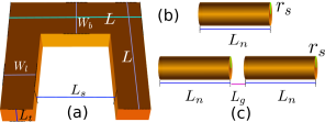
For our first example of the QNM calculation of EELS, we study the gold SRR, which is the basic “artificial atom” unit cell of the negative index metamaterial, with a rich magnetic response to external electromagnetic fields SRREELSex ; DGTD2 ; VEELSGordon . While the 2D metamaterial lattice is usually fabricated on a low index semiconductor, for the present study, we will ignore the effects of the substrate and assume the SRR is in free space (), though this is not a model restriction. The SRR with thickness, nm, is located in -plane as is shown in Fig. 1(a) with parameters nm, nm, nm and nm.
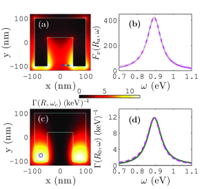
A full dipole FDTD calculation quasi2 ; FDTD shows that the dipole resonance of the QNM is around THz with mode profile shown in Fig. 2(a). We use an -polarized spatial plane wave with central frequency around 216 THz and pulse width fs, which is injected along the -axis; a running Fourier transform with a temporal bandwidth quasi2 fs is used to obtain the QNM. The corresponding effective mode volume (which is complex in its generalized form Philip ) is around at the chosen dipole position nm where (the dipole is shown by the blue arrow in Fig. 2(a), and note we have set the center of the SRR as the origin of the coordinate system). In order to first check the accuracy of the QNM calculation, we calculate the enhancement of the projected LDOS (or SE enhancement of a dipole emitter) from Eq. (4). Figure 2(b) shows that the single QNM model calculation (magenta solid, with Eq. (2)) agrees very well with the full numerical dipole calculation using FDTD RaoPRL ; YaoLaser ; ColeOL (grey dashed) at position . As is shown above, due to the strong confinement of the LSP, extremely small mode volumes are obtained leading to a strong enhancement of SE of an electric dipole (or single photon emitter) at this near field spatial position. The broad bandwidth of the SE enhancement is also a notable feature of metallic nanoresonators, making it much easier to spectrally couple to artificial atoms. We further remark that the spatial dependent spectral function, , as is discussed in Ref. Ourprb15 ; plasmonresonance , usually has a non-Lorentzian lineshape that in general changes as a function of position; this effect is captured by the QNM technique Ourprb15 through the spatial dependent phase factor of the QNM.
Due to the collective motion of the free electrons, there is an oscillating electric current circling along the SRR; as a result, a temporarily non-zero magnetic dipole is created, which displays a strong magnetic response to external electromagnetic field around the resonance of the QNM and forms the basis of exciting optical properties of metamaterial such as negative index. The working region of the SRR could be controlled by changing the length of the SRR which determines the QNM resonance.
The 2D EELS image, for a high energy, 100 keV, () electron beam injected along -axis is shown in Fig. 2(c), with , which is consistent with the calculations in Refs. SRREELSex ; DGTD2 ; VEELSGordon using full FDTD, nodal DGTG, and BEM, respectively. The EELS at the position of the blue circle (near a maximum field position) is obtained as shown in Fig. 2(d) by the dark green solid line as a function of the frequency; clearly the EELS can be used to effectively explore the QNM response of the plasmonic resonator. The magenta dashed line in Fig. 2(d) shows that the SE enhancement example almost has the same spectral lineshape as the spatially averaged EELS calculation.
V.2 Gold nanorod
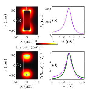
For our second example, we consider a single nanorod as is shown in Fig. 1(b), with radius nm and length nm. Frequently such nanorods are embedded inside liquids, so we assume the nanorod is located inside a homogeneous background medium with . Using FDTD simulations, the dipole resonance is found around THz quasi . In order to get the QNM, a -polarized spatial plane wave with central frequency 325 THz and fs is injected along -direction, and the running Fourier transform with fs is employed Ourprb15 . Figure 3(a) shows the mode profile of and the effective mode volume is found around ; the enhancement of the projected LDOS at position nm is shown in Fig. 3(b) (see arrow for dipole position), and the QNM calculation (magenta solid) shows excellent agreement with the full numerical calculation (grey dashed). The corresponding 2D EELS for an injected electron beam with energy keV is shown in Fig. 3(c) at the resonance frequency, THz. At the in-plane position nm, around which the maximum of the EELS is obtained (blue circle in Fig. 3(c)), is shown by the blue solid line in Fig. 3(d). It can be seen that the EELS again picks up the correct resonant response of the QNM. As is shown in Fig. 4(d), by the magenta dashed line, the SE enhancement now has a different lineshape than the EELS calculation; as discussed earlier, this is caused by the spatially varying nature of spectral lineshape.
V.3 Gold nanorod dimer
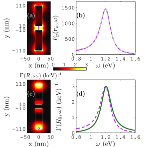
For our final resonator example, we study a dimer composed of two identical gold nanorods in homogeneous background with as is shown in Fig. 1(c). The eigenfrequency of the dipole mode is found at THz quasi2 , and the correspondent QNM, is shown in Fig. 4(a). Here in order to obtain the QNM mode, a -polarized plane wave with central frequency 291 THz and fs is injected, and fs is used for the running Fourier transform quasi2 . The effective mode volume at nm is found to be ; the enhancement of the LDOS, at , using QNM and full numerical FDTD calculations are shown by the magenta solid and gray dashed in Fig. 4(b), respectively. The 2D EELS, is shown in Fig. 4(c) at THz, for injected electrons with energy keV; at nm (blue circle in Fig. 4(a)) is shown by the dark green solid line in Fig. 4(d); once again we see that the SE enhancement (magenta dashed line) displays a rather different lineshape compared to EELS calculation, similar to the case of the single nanorod. The SE enhancement is also much larger for the dimer which also has a larger output coupling efficiency quasi2 .
As is shown in Ourprb15 , due to the inherent loss of the plasmonic system, the normalized QNM is in general complex, , and one obtains a position dependent phase factor , which induces both the reshaping of the spectrum of LDOS (that is proportional to the imaginary part of the Green function) and the variation of the position of peak; this causes the spectral lineshape between the EELS and the enhancement of LDOS to differ in general.
VI Discussion
It is important to stress that for the QNM calculation of EELS, one only needs two simulations to get the complex eigenfrequency and spatial distribution of the QNM (or QNMs), respectively. The rest of the calculation can be done semi-analytically with Eq. (2). Consequently, the QNM technique for EELS is many orders of magnitude faster than full FDTD calculation using electric dipoles, and offers more insight. Furthermore, by obtaining the magnetic field component of the QNM, i.e., , the magnetic Green function, could be calculated just as easily as the electric Green function; this can be used to simulate vortex-EELS as done in Ref. VEELSGordon which used brute force FDTD simulations. The QNM could also be applied to model the electromagnetic force on atoms and nanostructures for optical trapping, which as input, usually requires the Maxwell stress tensor and/or the Green function NovotnyBook .
Recently, Guillaume et al. Guil proposed an efficient modal expansion DDA method to model EELS. They show that by choosing a small number, e.g., 3-10, of eigenvectors their eigenvector expansion technique could get good results with reasonable accuracy, and the number of usual DDA operations are decreased considerably. For certain geometries this approach may outperform a QNM FDTD computation, though it is not clear how general the approach is for various shaped resonators. The philosophy of the QNM approach is to use the source free eigenmode solutions, obtained here using FDTD with the aid of the modal response from a scattered plane wave quasi2 . As a result, when there are a few dominant QNMs around the frequency of interest, in principle a single FDTD simulation is enough to obtain the modes and Green function as long as the overlap between the modes and injected field is sufficient. Moreover, we stress that the QNM computation is not limited to the FDTD method, e.g., it can also be obtained using an efficient dipole excitation technique with COMSOL Bai . The typical time needed for our QNM calculations with a fine mesh size as small as 1 nm around the metal resonator, and total simulation volume 1-2 micron cubed, takes around several days on a high performance workstation. This is certainly not insignificant, however, having the full Green function as a function of position and frequency can then solve numerous problems without any more numerical simulations for the electromagnetic response.
Apart from an efficient calculation of EELS, the QNM Green functions that we use above can be immediately adopted to efficiently study quantum light-matter interactions and true regimes of quantum plasmonics with quantized fields. For example, using the quantization scheme of the electromagnetic field in lossy structures StefanPRA58 ; Dung98 ; WelschPRA99 ; ourPRBMollow , the interaction between a quantum dipole (two level atom with frequency and dipole ) and electric field operator in the rotating wave approximation (assuming no external field) is given by the interaction Hamiltonian ; where the electric field operator is , with the imaginary part of and is the collective excitation operator of the field and medium; and is the Pauli operator. we stress that the electromagnetic response of the lossy structure is rigorously included by the classical Green function (obtained from Eq. (2)). For example, in a Born-Markov approximation, the quantum dynamics of quantum emitters around a metal nanostructures can be described through a reduced density matrix whose coupling terms can be fully described, including emitter-emitter and emitter-LSP interactions, through the analytical properties of the QNM Green function. For example, a recent example study of the quantum dynamics between two plasmon-coupled quantum dots is shown in Ourprb15 . Note that such an approach is ultimately more powerful than a standard Jaynes-Cummings model since it can include non-Lorentzian decay processes and nonradiative coupling to the resonator in a self-consistent way, and it can also be used to improve the simpler Jaynes-Cummings models (in a regime where they are deemed to be approximately valid) with a rigorous definition of the various required coupling parameters Ourprb15 .
VII Conclusions
We have introduced an efficient and semi-analytic calculation technique for modelling EELS using a QNM expansion technique, and exemplified the approach for several different metallic nanostructures. We first showed that the QNM technique works well for the SRR, and demonstrated that the QNM could be used to obtain similar 2D EELS maps to those shown in Refs. SRREELSex ; DGTD2 ; VEELSGordon , but with orders of magnitude improvements in efficiency and deeper physical insight. We then showed QNM calculations for a single gold nanorod and dimer of gold nanorods. We also presented example Purcell factor calculations and demonstrated how the spectral profiles may differ to EELS.
Acknowledgements.
This work was supported by the Natural Sciences and Engineering Research Council of Canada and Queen’s University. We thank Philip Kristensen for useful discussions.References
- (1) E. C. Dreaden, A. M. Alkilany, X. Huang, C. J. Murphy, and M. A. El-Sayed, “ The golden age: gold nanoparticles for biomedicine,” Chem. Soc. Rev. 41, 2740 (2012).
- (2) K. Saha, S. S. Agasti, C. Kim, X. Li, and V. M. Rotello, “Gold nanoparticles in chemical and biological sensing” Chem. Rev. 112, 2739 (2005).
- (3) L. E. Kreno, K. Leong, O. K. Farha, M. Allendorf, R. P. Van Duyne, and J. T. Hupp, “Metal–Organic Framework Materials as Chemical Sensors,” Chem. Rev. 112, 1105 (2012).
- (4) C. Valsecchi, and A. G. Brolo, “Periodic Metallic Nanostructures as Plasmonic Chemical Sensors,” Langmuir 29, 5638 (2013).
- (5) S. F. Tan, L. Wu, J. K. W. Yang, P. Bai, M. Bosman, and C. A. Nijhuis, “Quantum plasmon resonances controlled by molecular tunnel junctions,” Science 343, 1496 (2014).
- (6) H. A. Atwater, and A. Polman, “Plasmonics for improved photovoltaic devices,” Nat. Mater. 9, 205 (2010).
- (7) Z. Guo, J. Hwang, B. Zhao, J. H. Chung, S. G. Cho, S.-J. Baek, and J. Choo, “Ultrasensitive trace analysis for 2,4,6-trinitrotoluene using nano-dumbbell surface-enhanced Raman scattering hot spots,” Analyst 139, 807 (2014).
- (8) E. Betzig, P. L. Finn, and J. S. Weiner, “Combined shear force and near-field scanning optical microscopy,” Appl. Phys. Lett. 60, 2484 (1992).
- (9) C. Chicanne, T. David, R. Quidant, J. C. Weeber, Y. Lacroute, E. Bourillot, A. Dereus, G. Cp;as des Francs, and C. Girard, “Imaging the Local Density of States of Optical Corrals” Phys. Rev. Lett. 88, 097402 (2002).
- (10) A. Drezet, A. Hohenau, D. Koller, A. Stepanov, H. Ditlbacher, B. Steinberger, F. R. Aussenegg, A. Leitner, and J. R. Krenn, “Leakage radiation microscopy of surface plasmon polaritons,” Mater. Sci. Eng. B 149, 220 (2008).
- (11) K. Imura, T. Nagahara, and H. Okamoto, “Near-field two-photon-induced photoluminescence from single gold nanorods and imaging of plasmon modes,” J. Phys. Chem. B 109, 13214 (2005).
- (12) S. Viarbitskaya, A. Teulle, R. Marty, J. Sharma, C. Girard, A. Arbouet, and E. Dujardin, “Tailoring and imaging the plasmonic local density of states in crystalline nanoprisms,” Nat. Mater. 12, 426 (2013).
- (13) A. Losquin, and M. Kociak, “Link between Cathodoluminescence and Electron Energy Loss Spectroscopy and the Radiative and Full Electromagnetic Local Density of States,” ACS Photonics 2, 1619 (2015).
- (14) J. Nelayah, M. Kociak, O. Stéphan, F. J. García de Abajo, M. Tencé, L. Henrard, D. Taverna, I. Pastoriza-Santos, L. M. Liz-Marzán, and C. Colliex, “Mapping surface plasmons on a single metallic nanoparticle,” Nat. Phys. 3, 348 (2007).
- (15) M. Bosman, V. J. Keast, M. Watanabe, A. I. Maaroof, and M. B. Cortie, “Mapping surface plasmons at the nanometre scale with an electron beam,” Nanotechnology 18, 165505 (2007).
- (16) F. J. García de Abajo, and M. Kociak, “Probing the Photonic Local Density of States with Electron Energy Loss Spectroscopy,” Phys. Rev. Lett. 100, 106804 (2008).
- (17) U. Hohenester, H. Ditlbacher, and J. R. Krenn, “Electron-Energy-Loss Spectra of Plasmonic Nanoparticles,” Phys. Rev. Lett. 103, 106801 (2009)
- (18) F. J. García de Abajo, “Optical excitations in electron microscopy,” Rev. Mod. Phys. 82, 209 (2010).
- (19) M. Husnik, F. van Cube, S. Irsen, S. Linden, J. Niegemann, K. Busch and M. Wegener, “Comparison of electron energy-loss and quantitative optical spectroscopy on individual optical gold antennas,” Nanophotonics 2, 241 (2013).
- (20) O. Nicoletti, M. Wubs, N. A. Mortensen, W. Sigle, P. A. van Aken, and P. A. Midgley, “Surface plasmon modes of a single silver nanorod: an electron energy loss study,” Opt. Express 19, 15371 (2011).
- (21) D. Rossouw, M. Couillard, J. Vickery, E. Kumacheva, and G. A. Botton, “Multipolar Plasmonic Resonances in Silver Nanowire Antennas Imaged with a Subnanometer Electron Probe,” Nano Lett. 11 1499 (2011).
- (22) M. Uchida, and A. Tonomura, “Generation of electron beams carrying orbital angular momentum,” Nature 464, 737 (2010).
- (23) J. Verbeeck, H. Tian, and P. Schattschneider, “Production and application of electron vortex beams,” Nature 467, 301 (2010).
- (24) Z. Mohammadi, C. Van Vlack, S. Hughes, J. Bornemann, and R. Gordon, “Vortex Electron Energy Loss Spectroscopy for Near-Field Mapping of Magnetic Plasmons,” Opt. Express 20, 15024 (2012).
- (25) F. Ouyang, and M. Issacson, “Accurate modeling of particle-substrate coupling of surface plasmon excitation in EELS,” Ultramicroscopy 31, 345 (1989).
- (26) F. J. García de Abajo, and J. Aizpurua, “Numerical simulation of electron energy loss near inhomogeneous dielectrics,” Phys. Rev. B 56, 15873 (1997).
- (27) F. J. García de Abajo, and A. Howie, “Retarded field calculation of electron energy loss in inhomogeneous dielectrics,” Phys. Rev. B 65, 115418 (2002).
- (28) U. Hohenester, “Simulating electron energy loss spectroscopy with the MNPBEM toolbox,” Comp. Phys. Commun. 185, 1177 (2014).
- (29) L. Henrard, and P. Lambin, “Calculation of the energy loss for an electron passing near giant fullerenes,” J. Phys. B 29, 5127 (1996).
- (30) C. Matyssek, J. Niegemann, W. Hergert, and K. Busch, “Computing electron energy loss spectra with the Discontinuous Galerkin Time-Domain method,” photon. Nanostruct.: Fundam. Appl. 9, 367 (2011).
- (31) F. Von Cube, S. Irsen, J. Niegemann, C. Matyssek, W. Hergert, K. Busch, and S. Linden, “Spatio-spectral characterization of photonic meta-atoms with electron energy-loss spectroscopy,” Opt. Mater. Express 1, 1009 (2011).
- (32) Y. Cao, A. Manjavacas, N. Large, and P. Nordlander, “Electron Energy-Loss Spectroscopy Calculation in Finite-Difference Time-Domain Package,” ACS Photonic 2, 369 (2015).
- (33) K. J. Savage, M. M. Hawkeye, R. Esteban, A. G. Borisov, J. Aizpurua, and J. J. Baumberg, “Revealing the quantum regime in tunnelling plasmonics,” Nature 491, 574 (2012).
- (34) R. Esteben, A. G. Borisov, P. Nordlander, and J. Aizpurua, “Bridging quantum and classical plasmonics,” Nat. Commun. 3, 825 (2012).
- (35) N. A. Mortensen, S. Raza, M. Wubs, T. Søndergaard, and S. I. Bozhevolnyi, Nat. Commun. “ A generalized non-local optical response theory for plasmonic nanostructures,” 5, 3809 (2014).
- (36) G. Hajisalem, M. S. Nezami, and R. Gordon, “Probing the quantum tunneling limit of plasmonic enhancement by third harmonic generation,” Nano Lett. 14, 6651 (2014).
- (37) T. Christensen, W. Yan, S. Raza, A.-P. Jauho, N. A. Mortensen, and M. Wubs, “Nonlocal Response of Metallic Nanospheres Probed by Light, Electrons, and Atoms,” ACS Nano 8, 1745 (2014).
- (38) Søren Raza1, Shima Kadkhodazadeh, Thomas Christensen, Marcel Di Vece, Martijn Wubs, N. Asger Mortensen, and Nicolas Stenger, “Multipole plasmons and their disappearance in few-nanometre silver nanoparticles,” Nature Communications 6, 1 (2015).
- (39) A. Hörl, A. Trügler, and U. Hohenester, “Full Three-Dimensonal Reconstruction of the Dyadic Green Tensor from Electron Energy Loss Spectroscopy of Plasmonic Nanoparticles,” ACS Photonics 2, 1429 (2015).
- (40) G. Boudarham, and M. Kociak, “Modal decompositions of the local electromagnetic density of states and spatially resolved electron energy loss probability in terms of geometric modes,” Phys. Rev. B 85, 245447 (2012).
- (41) R.-C. Ge, P. T. Kristensen, J. F. Young, and S. Hughes, “Quasinormal mode approach to modelling light-emission and propagation in nanoplasmonics,” New J. Phys. 16, 113048 (2014).
- (42) R.-C. Ge, and S. Hughes, “Design of an efficient single photon source from a metallic nanorod dimer: a quasi-normal mode finite-difference time-domain approach,” Opt. Lett. 39, 4235 (2014).
- (43) H. M. Lai, P. T. Leung, K. Young, P. W. Barber, and S. C. Hill, “Time-independent perturbation for leaking electromagnetic modes in open systems with application to resonances in microdroplets,” Phys. Rev. A 41, 5187 (1990).
- (44) P. T. Leung, S. Y. Liu, and K. Young, “Completeness and time-independent perturbation of the quasinormal of an absorptive and leaky cavity,” Phys. Rev. A 49, 3982 (1994).
- (45) P. T. Kristensen, and S. Hughes, “Modes and Mode Volumes of Leaky Optical Cavities and Plasmonic Nanoresonators,” ACS Photonics 1, 2 (2014).
- (46) C. Sauvan, J. P. Hugonin, I. S. Maksymov, and P. Lalanne, “Theory of the Spontaneous Optical Emission of Nanosize Photonic and Plasmon Resonators,” Phys. Rev. Lett. 110, 237401 (2013).
- (47) P. T. Kristensen, R.-C. Ge, and S. Hughes, “Normalization of quasinormal modes in leaky optical cavities and plasmonic resonators,” Phys. Rev. A 92, 053810 (2015).
- (48) We use FDTD Solutions: www.lumerical.com.
- (49) P. Gay-Balmaz, and O. J. F. Martin, “Electromagnetic scattering of high-permittivity particles on a substrate,” Appl. Opt. 40, 4562 (2001).
- (50) The contribution of image charge when the electron coming to the slab is to accelerate the electron, while it will decelerate the electron when the electron is leaving the other side of the slab. Both process will be antisymmetric of each other since we have assume the speed change of the process is negligible with high energy electrons; as a result, they would cancel each other.
- (51) R. Ge, Jeff F. Young, and S. Hughes, “Quasi-normal mode approach to the local-field problem in quantum optics,” Optica 2, 246 (2015).
- (52) G. Boudarham, N. Feth, V. Myroshnychenko, S. Linden, J. García de Abajo, M. Wegener, and M. Kociak, “Spectral Imaging of Individual Split-Ring Resonators,” Phys. Rev. Lett. 105, 255501 (2010).
- (53) V. S. C. Manga Rao, and S. Hughes, “Single quantum dot spontaneous emission in a finite-size photonic crystal waveguide: Proposal for an efficient ”on chip” single photon gun,” Phys. Rev. Lett. 99, 193901 (2007).
- (54) P. Yao, V. S. C. Manga Rao, and S. Hughes, “On-chip single photon sources using planar photonic crystals and single quantum dots, ” Laser Photon. Rev. 4, 499 (2010).
- (55) C. Van Vlack, and S. Hughes, “Finite-difference time-domain technique as an efficient tool for obtaining the regularized Green function: applications to the local field problem in quantum optics for inhomogeneous lossy materials,” Opt. Lett. 37, 2880 (2012).
- (56) R.-C. Ge, and S. Hughes, “Quantum dynamics of two quantum dots coupled through localized plasmons: An intuitive and accurate quantum optics approach using quasinormal modes,” Phys. Rev. B 92, 205420 (2015).
- (57) G. W. Bryant, F. J. García de Abajo, and J. Aizpurua, “Mapping the Plasmon Resonances of Metallic Nanoantennas,” Nano Lett. 8, 631 (2008).
- (58) e.g., see L. Novotny, and B. Hecht, Principles of Nano-Optics, Cambridge University Press (2012).
- (59) S.-T. Guillaume, F. J. García de Abajo, and L. Henrard, “Efficient modal-expansion discrete-dipole approximation: Application to the simulation of optical extinction and electron energy-loss spectroscopies,” Phys. Rev. B 88, 245439 (2013).
- (60) Q. Bai, M. Perrin, C. Sauvan, J-P Hugonin, and P. Lalanne, “Efficient and intuitive method for the analysis of light scattering by a resonant nanostructure,” Opt. Express 21 27371 (2013).
- (61) S. Scheel, L. Knöll, and D-G. Welsch, “QED commutation relations for inhomogeneous Kramers-Kronig dielectrics,” Phys. Rev. A 58, 700 (1998)
- (62) H. T. Dung, L. Knöll, and D.-G. Welsch, “Three-dimensional quantization of the electromagnetic field in dispersive and absorbing inhomogeneous dielectrics,” Phys. Rev. A 57, 3931 (1998).
- (63) S. Scheel, L. Knöll, and D.-G. Welsch, “Spontaneous decay of an excited atom in an absorbing dielectric,” Phys. Rev. A 60 4094 (1999).
- (64) Rong-Chun Ge, C. Van Vlack, P. Yao, Jeff. F. Young, S. Hughes, “Accessing quantum nanoplasmonics in a hybrid quantum-dot metal nanosystem: Mollow triplet of a quantum dot near a metal nanoparticle,” Phys. Rev. B 87, 205425 (2013).