A Low-Noise CMOS Pixel Direct Charge Sensor, Topmetal-II-
Abstract
We report the design and characterization of a CMOS pixel direct charge sensor, Topmetal-II-, fabricated in a standard CMOS Integrated Circuit process. The sensor utilizes exposed metal patches on top of each pixel to directly collect charge. Each pixel contains a low-noise charge-sensitive preamplifier to establish the analog signal and a discriminator with tunable threshold to generate hits. The analog signal from each pixel is accessible through time-shared multiplexing over the entire array. Hits are read out digitally through a column-based priority logic structure. Tests show that the sensor achieved a analog noise and a minimum threshold for digital readout per pixel. The sensor is capable of detecting both electrons and ions drifting in gas. These characteristics enable its use as the charge readout device in future Time Projection Chambers without gaseous gain mechanism, which has unique advantages in low background and low rate-density experiments.
keywords:
Topmetal , Pixel , Charge sensor , Ion readout1 Introduction
Over the years a number of highly pixelated CMOS sensors and readout Integrated Circuit (IC) chips have been developed and deployed successfully in nuclear and particle physics experiments. Notable examples are CMOS readout pixel ICs such as Medipix/Timepix[1, 2] and FE-I3/FE-I4 [3], and Monolithic Active Pixel Sensors (MAPS) such as the one described in [4]. Readout pixel ICs are designed mainly to be coupled to external solid state detectors through processes such as flip-chip bump bonding. Charges are generated in the external detector due to the passing of ionizing particles, then collected and measured by the readout IC. MAPS ICs allow charges to be generated inside of the silicon IC (pixel) itself and integrate the readout circuitry in the same chip.
The high pixel density and high integration of circuitry nature of pixel ICs made them appealing to be the charge readout device of choice in Micro-Pattern Gaseous Detectors (MPGDs)[5], replacing conventional wire readout schemes[6] and patterned Printed Circuit Board (PCB) readout schemes[7]. These MPGDs are usually used for charge and timing measurements in Time Projection Chambers (TPCs)[8] achieving improved spatial resolution and noise performance. For instance, the D3 experiment [9] uses FE-I3/FE-I4 sensors developed for the ATLAS [10] experiment, behind a Gaseous Electron Multiplication (GEM) stage, to detect charge tracks resulting from potential dark matter interactions. Some similar efforts using the Timepix sensor behind GEMs were presented in [11, 12]. A more integrated approach, fabricating a micro-pattern gaseous gain structure directly on top of a Medipix/Timepix chip by means of wafer post-processing, was reported in [13] (InGrid).
In these applications of pixel ICs in gaseous detectors, ICs were usually designed for a different purpose and were later converted to perform direct charge readout resulting in characteristic mismatches between the IC performance and application requirements. Very few direct charge collection ICs were designed specifically for micro-pattern gaseous pixel detectors. A notable exception is an IC described in [14] that is dedicated to GEM readout and X-ray polarimetry applications[15].
Regardless of which IC is employed for charge readout, an electron gas-avalanche gain stage is involved in all the above mentioned pixel readout systems. These systems are generally geared towards detectors for high event rate and high electron drift speed. An electron gas-avalanche gain is necessary to amplify the number of electrons to be well above the noise of ICs. Also, a pulse shaper is normally built in-chip to increase the rate capabilities. On the other hand, there is a class of measurements that disfavor the use of gas-avalanche gain while demand similar spatial and timing resolution. They are usually low rate-density (event rate per volume) and low background experiments. Examples are alpha particle counting[16], neutrinoless double-beta decay () searches by drifting ions in a high pressure TPC[17, 18], upgrades to ion chambers for beam measurements, and advanced electron-track gamma-ray imaging[19]. Gas-avalanche gain is disfavored due to its large gain fluctuation and sparking resulting in poor energy resolution and stability issues particularly in large-area readout systems. Also, positive ions and negative ions in high pressure gas cannot undergo gas-avalanche. High spatial resolution is required for imaging, position determination and interaction vertex identification.
We designed a CMOS IC, Topmetal-II-, that is uniquely suitable for charge measurement in a TPC without gas-avalanche gain. It is a direct charge sensor with pitch between pixels fabricated in a standard CMOS process without post-processing. A metal patch is placed on the top of each pixel (Topmetal) in a pixel array for charge collection. Each pixel contains a low-noise charge-sensitive preamplifier (CSA) to establish the analog signal and a discriminator with tunable threshold to generate hits. For its intended application, event-rate density is expected to be low and charge (both free electron and ion) drifting speed is expected to be slow; therefore, we tuned the preamplifier to have long signal retention and eliminated the in-chip pulse shaper while focusing on improving the noise performance. The analog signal from each pixel is accessed through time-shared multiplexing over the entire array. Hits are read out digitally through a column-based priority logic structure.
In this paper we present the overall design and some initial test results of Topmetal-II-. The implementation of the charge collection electrode and a time-shared analog multiplexing structure have been validated in our earlier IC development Topmetal-I [20]. We will focus on the analog characteristics from CSA and the behavior of digital readout. Details on circuitry and specific application notes will be presented elsewhere.
2 Sensor Structure and Operation
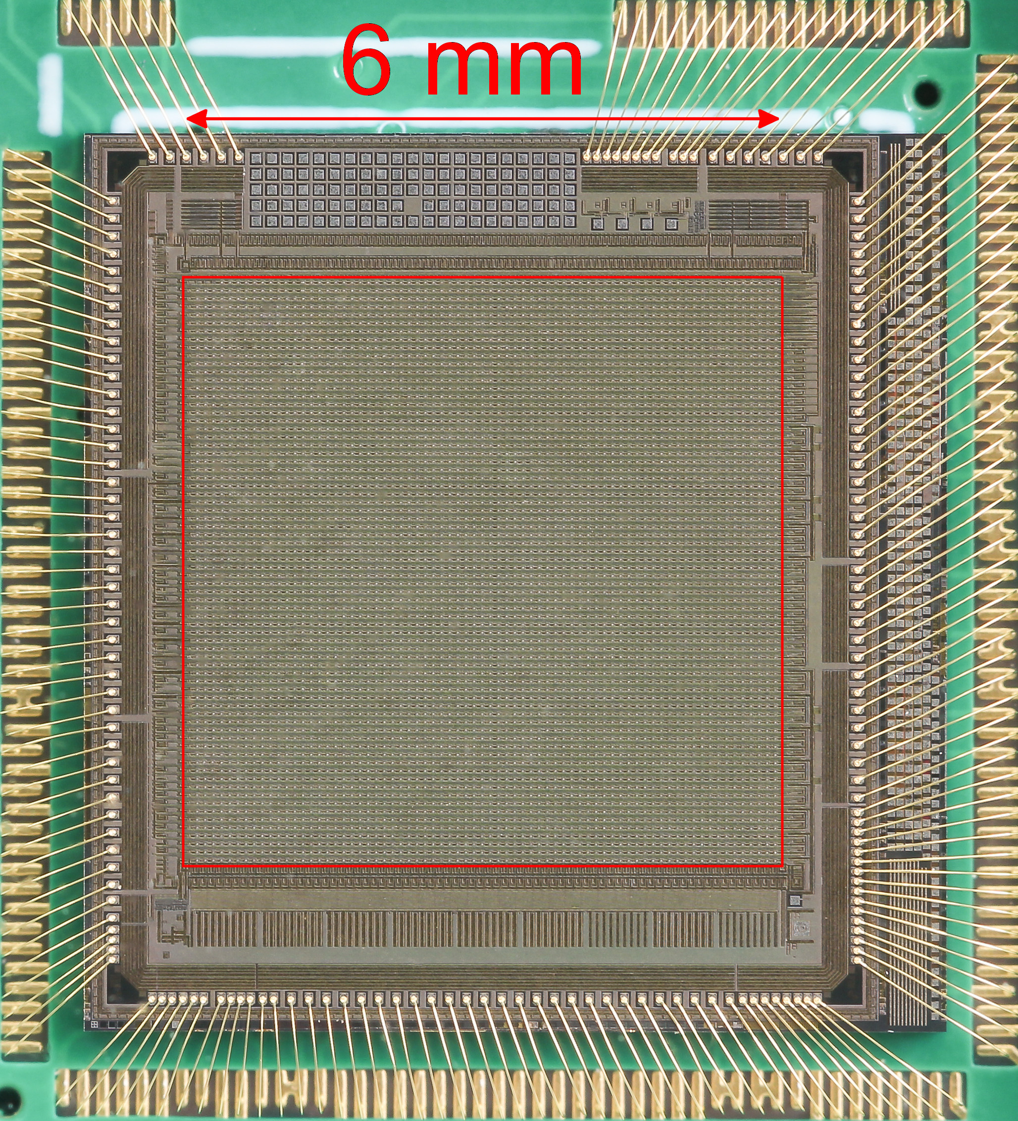
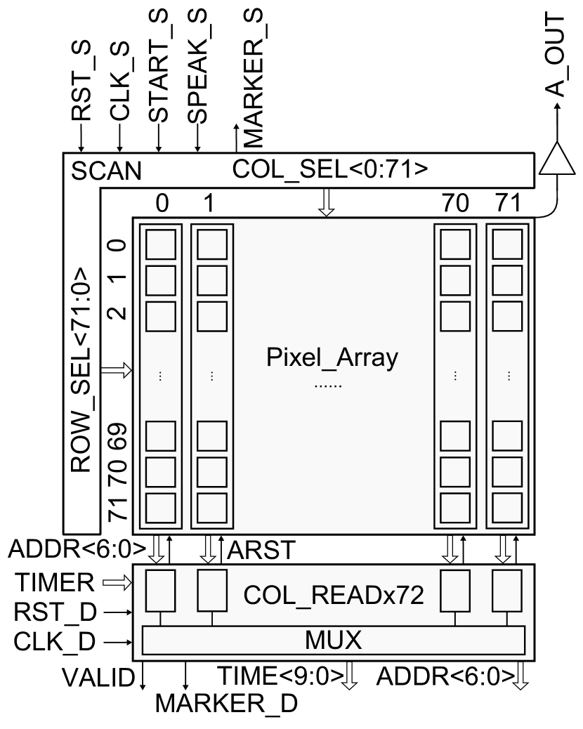
A photograph of one wire-bonded Topmetal-II- sensor is shown in Fig. 1 (left). The sensor is implemented in a silicon real-estate area. A schematic view of the sensor architecture is shown in Fig. 1 (right). With pitch distance between pixels, the square pixel array makes up a charge sensitive region. Readout interface logic and an analog buffer are placed adjacent to the pixel array. The sensor is powered by analog supply AVDD and digital supply DVDD, which are individually regulated at a nominal voltage of .
Each pixel collects charges via its own sized metal node (Topmetal), then converts them to both analog and digital signals (Fig. 2). Separate circuit structures read out both analog and digital signals from every pixel and send them through dedicated channels to external interfaces. The pixel structure, analog, and digital readouts are described in the following subsections.
2.1 Pixel Structure
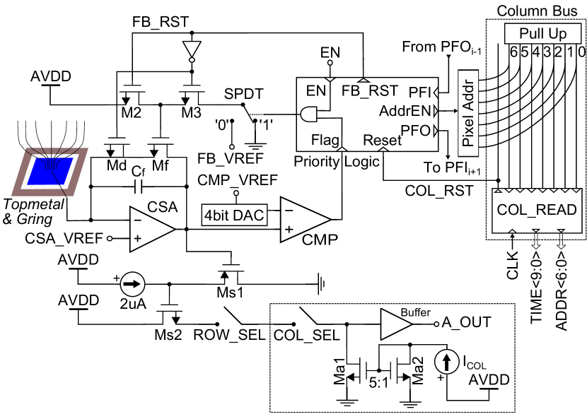
A schematic view of the internal structure of a single pixel is shown in Fig. 2. The Topmetal is directly connected to the input of the CSA. Around the Topmetal there is a “Guard Ring” (Gring), which is a ring electrode in the same topmost metal layer as the Topmetal but isolated from it. Gring serves a dual purpose. Firstly, when biased to a different electric potential than the Topmetal, an electric field gradient is formed around the Topmetal, which focuses the moving charges hence enhances the charge collection efficiency. Secondly, the stray capacitance between the Gring and the Topmetal, , is a natural test capacitor. It allows us to apply pulses on Gring to inject signals into the CSA to measure its performance. The parametric extraction from the IC design software as well as an independent Finite Element Analysis (FEA) show that .
The CSA is a dual-input folded cascode Operational Amplifier (OpAmp) with capacitive feedback (Fig. 3). The parasitic capacitance of the Topmetal to ground, plus the gate capacitance of M1, is about , which is presented to the CSA as its input capacitance. The reference voltage sets the baseline voltage of the Topmetal. The feedback capacitor is implemented using the stray capacitance between two metal traces. We estimate from parametric extraction in the IC design software. During normal analog-only operations (EN=0,FB_RST=0), a fine-adjusted voltage FB_VREF is applied through M3 in Fig. 2 onto the gate of Mf, which sets the equivalent feedback resistance ( of Mf). The gate-source voltage of Mf is determined by . We usually set to a few hundred , which is sub-threshold for Mf and results in a large . Consequently, the feedback time constant can be as large as seconds, and it can be adjusted by varying . Md is a “dummy” transistor that does not affect normal analog operations. However during digital readout, we utilize its gate capacitance to counteract the charge injection from Mf during switching.

We designed the CSA to be particularly low in power consumption ( per CSA) and intentionally limited its bandwidth to below . Low bandwidth reduces noise. Also, low bandwidth results in slow rise of signal upon charge arrival. Combined with the large , which ensures long signal retention, the output of CSA can be multiplexed and sampled slowly without going through an anti-alias filter or an in-pixel shaper. The entire analog channel is DC coupled. The CSA output is also DC coupled to the discriminator. DC coupling is necessary to handle slowly varying signals.
The comparator compares the CSA output to a set threshold provided by a 4-bit DAC in each pixel. All the 4-bit DACs in the entire array share a common offset that is settable externally. The finest step of each 4-bit DAC is tuned to be so that the entire dynamic range of the DAC () could cover the dispersion of the comparator input across the array. When the CSA output surpasses the threshold, a hit is generated and the Priority Logic Module is notified by the Flag signal.
There is a 5-bit SRAM in each pixel. 4 bits are for setting the value of the DAC. The fifth bit controls the digital EN. The SRAM can be written into when the pixel is selected during analog multiplexing via ROW_SEL and COL_SEL. SRAM was chosen over D Flip-Flop to save the floor space.
2.2 Analog Readout
The analog output from the CSA in each pixel goes through two source-follower stages (Ms1 and Ms2 in Fig. 2) before entering the analog output buffer that drives the signal off-chip for the entire array (lower dashed box in Fig. 2). A time-shared multiplexing scheme is used to readout the entire array. A Scan Module controls the row selection switch (ROW_SEL) and the column selection switch (COL_SEL) to select one pixel at a time for its analog signal to pass through to the output buffer. Each pixel has a set of Ms1, Ms2, and the ROW_SEL switch. Each column shares one COL_SEL switch. The entire sensor has one output buffer and one pair of Ma1 and Ma2. The first stage source-follower Ms1 and its bias is constantly on for all the pixels while the second stage source follower is only on for the single chosen pixel in multiplexing. Since the CSA has very limited drive strength, it is easily affected by the row and column switching. The addition of the first stage source-follower is necessary to isolate the switches from the CSA.
Switches operate at every rising edge of the clock fed into the Scan Module. The behavior of the analog output during pixel switching is shown in Fig. 7. The Scan Module accepts a clock of frequency ranging from 0 to tens of . We could supply a controlled number of cycles of clock, then completely stop the clock, in order to select a desired pixel to be connected statically to the output buffer. This feature was exploited during analog noise measurements.
2.3 Digital Readout
When EN=1, the Priority Logic Module in each pixel will respond to the output of the comparator (Flag), which becomes 1 when the CSA output exceeds the set threshold. The Priority Logic Module is a combinational logic that controls the reset (FB_RST) of the CSA upon a hit and drives the hit information through the column readout structure. Its behavior is governed by Eq. 1
| (1a) | ||||
| PFO | (1b) | |||
| AddrEN | (1c) | |||
| FB_RST | (1d) | |||
where is an intermediate variable.
Pixels are arranged and interconnected in columns. For the th pixel, its PFIi is connected to the previous (th) pixel’s PFOi-1, and its PFOi is fed into the next (th) pixel’s PFIi+1. Pixels in the same column are daisy-chained in this fashion. Each pixel in the same column has a unique 7-bit address. The address controller in each pixel is connected to an address bus common to a column. The address bus is normally pulled up to all 1. When AddrEN is active in a pixel, said pixel pulls down the address bus to its own unique address. A common COL_RST is sent from the COL_READ module to the Reset port of every pixel in the column simultaneously (Fig. 2).
The top-most pixel (0th) in a column has PFI. When there is no hit in any pixel, the propagation of Eq. (1b) dictates that every pixel in the column has . When the th pixel gets a hit, hence . Due to Eq. (1b), all pixels below the th pixel (denoted by th, ) will have . Due to Eq. (1c), any pixel with won’t enable AddrEN even if it gets a hit. This logic describes a priority chain of pixels: the pixel with a hit that has the lowest (highest priority) could enable AddrEN, and it disables all the pixels lower in the chain from reacting to hits. An associated consequence is that the address bus is pulled down by only one pixel (the highest priority pixel with a hit) so that no race condition rises on the address bus.
The COL_READ module monitors the address bus. It reacts to the address change on the bus, then reads the hit and resets the pixel. A digital multiplexer (MUX in Fig. 1 (right)) polls the status of each COL_READ module sequentially once per clock cycle. It assembles the hit pixel address and the hit time data, then ships them off the sensor.

A timing diagram of a hit-read-reset cycle is shown in Fig. 4. Charges arrive at , causing the CSA output to exceed the threshold, generating a hit (). Activated by , a single-pole-double-throw (SPDT) switch grounds the gate of Mf from its original bias FB_VREF, so the CSA maximally retains the charge signal. Since there is no higher-priority pixel () and this pixel is enabled (), , PFO and AddrEN become 1 accordingly. At this moment the address bus is pulled to the address of this pixel as well. At (rising edge of the clock in the COL_READ module), the COL_READ module senses the address change; then, it waits for 4 clock cycles to make sure the address change is not a transient phenomenon. At the end of the waiting period, , the COL_READ module registers the time from a system timer (counter) and sends a reset signal to Reset. Although Reset is sent to every pixel in the column, due to Eq. (1d), only the pixel that is pulling the address bus and is being read out will respond to the reset. The reset sets , which turns on the feedback transistor Mf to discharge so that the CSA output comes down towards the baseline. At , the CSA output falls below the threshold causing hence FB_RST is removed. Reset is removed when the COL_READ module is polled (). The time between and is non-deterministic and can be as high as 72 clock cycles.
When multiple pixels in the same column are hit simultaneously, the logic reads out and resets the hit pixels sequentially in an order following their priorities. Eq. (1a) ensures that when a higher-priority hit pixel is reset, the next-priority hit pixel is not reset until Reset is toggled. No hit is missed; however, the timing is only accurate for the pixel with the highest priority. The timing resolution is determined by the system timer (counter) frequency.
It is worth noting that no digital clock is sent into the array. Clock is only fed to the COL_READ module at the bottom of each column. The digital logic in the array is entirely combinational and asynchronous. This design minimizes the interference between digital logic and the analog circuit. Tests show that this readout implementation works correctly as designed.
Column-based readout structures have been realized in several ICs such as [21, 22, 23]. Unique addresses for pixels and the propagation of priorities, sometimes called tokens, were also used. The major difference in this design is that a reset signal is required to be sent into the pixel being read out to bring the CSA output down below the threshold. We implemented the logic to handle this requirement correctly.
3 Test results
All the following tests were conducted at room temperature in ambient air.
3.1 Analog noise measurement
We applied a calibrated square wave on the guard ring. The square wave has a peak-to-peak amplitude of . Since there is a coupling capacitance, , between the Gring and the CSA input, at each transition edge of the square wave, an equivalent charge is injected into the CSA. At a rising edge of the square wave, positive equivalent charge is injected. Negative equivalent charge is injected at a falling edge. The CSA responds to both polarities equally well; however, we focus on the negative equivalent charge in this measurement. The frequency of the square wave is chosen to be low enough so that the CSA output has sufficient time to fall back to the baseline before the next transition arrives.
We utilized the pixel selection feature of the Scan Module to stop at a pixel and digitize its analog output continuously. An example of the CSA output response to a negative charge injection is shown in Fig. 5. Since the entire analog channel is DC coupled, the baseline is at a value determined by CSA_VREF and level-shifts from source followers. As expected, the CSA output rises sharply upon the arrival of a pulse, then decays down towards the baseline exponentially with a time constant determined by , which is in the range of several milliseconds.

Traditionally the noise performance of a CSA is reported as the fluctuation of the pulse height after a shaper. Since we do not have a shaper in the sensor, we applied a digital trapezoidal filter[24] in software. The trapezoidal filter automatically zeros the baseline of its output. We shifted the filter output to match the baseline of the CSA output for better graphical comparison. The flat-top part of the trapezoidal filter output is used to evaluate the height of the pulse. By collecting many pulses, we show that the pulse height has a mean value and a standard deviation . The charge conversion gain is then evaluated as and the Equivalent Noise Charge (ENC) is .
Although the amplitude of the square wave is calibrated, we acknowledge that is not independently calibrated and that its value is entirely from simulation albeit both the IC design software and an FEA analysis gave consistent results. Nevertheless, we report on the noise measurement based on the simulation result of and note it as the sole source of uncertainty in the noise value. The reported noise includes noise from the entire data acquisition chain; therefore, it is an upper limit of the true noise in the sensor.
Using the same data, by collecting many baseline samples before the rise in the CSA output, we obtain a standard deviation of of the baseline, which is equivalent to using the above computed charge conversion gain. The baseline fluctuation determines the minimum threshold of the discriminator. In this case, the finest adjustable step of the threshold is , determined by the in-pixel DAC, which is 5 times the standard deviation of the baseline. Therefore we estimate the minimum threshold to be .
3.2 Alpha induced charge tracks in ambient air
We installed a thin metal plate, biased at relative to the sensor ground, above and parallel to the top surface of a Topmetal-II- sensor. The entire setup is in ambient air (Fig. 6). A nearly uniform electric field of is generated between the plate and the sensor. A through-hole in the plate is aligned with the center of the sensor. A spectroscopic 241Am alpha source with a thin window is placed on the plate above the through-hole so that alpha particles could travel through the hole towards the sensor and ionize air along the tracks. The through-hole coarsely collimates the alpha particles to a general downward-going direction towards the sensor; however, it allows some divergence so that alphas have a probability to travel sideways. The 241Am alpha source emits alphas that range out at about in air; therefore, no alpha particle directly hits the sensor. The ionization charges, which are believed to be mostly ions in air, drift slowly in the electric field at a speed of several [25].

We operated the Topmetal-II- sensor at an identical setting as in the noise measurement, . Digital modules were entirely turned off by setting in each pixel. A clock was supplied to the Scan Module to drive the analog multiplexing. Under such clock frequency, each pixel occupies in the analog output of the array, and it takes to scan all of the pixels once (one frame). Effectively each pixel is sampled once every , and each sampling lasts . We used an external digitizer working at to record the multiplexed analog output. The Scan Module clock is derived from the digitizer clock at ratio; hence, the two clocks are synchronized, and so each pixel is digitized exactly 4 times. We took the average of 2 samples in the middle as the digitization value for the pixel discarding the leading and trailing samples to eliminate the transition period at pixel switching. A data sample illustrating this sampling scheme is shown in Fig. 7.

After de-multiplexing in software, we obtain a continuous waveform for each pixel sampled at a rate of . There are independent waveforms for the entire array. Since the signal retention time of CSA is long (milliseconds), such low effective sampling rate is sufficient to capture charge signals. We applied a software trapezoidal filter to each waveform independently. For a given time (sample), the height of filter outputs from every pixel form an image. Alpha particle induced charge tracks are identified in these time dependent images. A set of images of a single track is shown in Fig. 8.
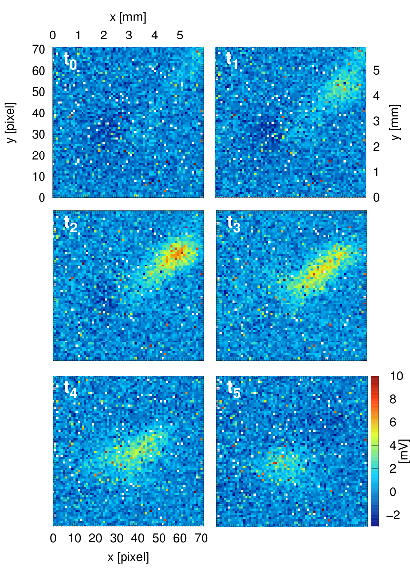
The setup constrains alpha tracks to be mostly perpendicular to the sensor surface with some inclination angle. When the leading part of the charge track arrives at the sensor, other parts are still away from the sensor. Due to the slow-moving nature of charges drifting in air, even at a sampling rate as slow as , the charge density variation due to the charge arrival time difference is visible in the data.
4 Summary
We have demonstrated the implementation of a highly pixelated sensor for direct charge collection and imaging using a standard CMOS technology. The combination of direct charge collection, low noise, and long signal retention makes the sensor appealing in several low background and low event-rate density applications involving slow-drifting ions without gaseous avalanche gain. A column based digital readout structure also allows hits to be registered efficiently.
To improve beyond Topmetal-II-, besides increasing the pixel density, we can further reduce the noise of the CSA. We will explore these options in future series of Topmetal sensors.
Acknowledgments
This work is supported, in part, by the Thousand Talents Program at Central China Normal University and by the National Natural Science Foundation of China under Grant No. 11375073. We also acknowledge the support from LBNL for hosting the physical measurements of the sensor. We would like to thank Christine Hu-Guo and Nu Xu for fruitful discussions.
References
- Ballabriga et al. [2011] R. Ballabriga, M. Campbell, E. Heijne, X. Llopart, L. Tlustos, W. Wong, Medipix3: A 64k pixel detector readout chip working in single photon counting mode with improved spectrometric performance, Nuclear Instruments and Methods in Physics Research Section A: Accelerators, Spectrometers, Detectors and Associated Equipment 633, Supplement 1 (0) (2011) S15 – S18, ISSN 0168-9002, URL http://www.sciencedirect.com/science/article/pii/S0168900210012982.
- Llopart et al. [2007] X. Llopart, R. Ballabriga, M. Campbell, L. Tlustos, W. Wong, Timepix, a 65k programmable pixel readout chip for arrival time, energy and/or photon counting measurements, Nuclear Instruments and Methods in Physics Research Section A: Accelerators, Spectrometers, Detectors and Associated Equipment 581 (1–2) (2007) 485 – 494, ISSN 0168-9002, URL http://www.sciencedirect.com/science/article/pii/S0168900207017020.
- Garcia-Sciveres et al. [2010] M. Garcia-Sciveres, et al., The FE-I4 pixel readout integrated circuit, Nucl. Instr. and Meth. A 636 (2010) S155–S159.
- Hu-Guo et al. [2010] C. Hu-Guo, J. Baudot, G. Bertolone, A. Besson, A. Brogna, C. Colledani, G. Claus, R. D. Masi, Y. Degerli, A. Dorokhov, G. Doziere, W. Dulinski, X. Fang, M. Gelin, M. Goffe, F. Guilloux, A. Himmi, K. Jaaskelainen, M. Koziel, F. Morel, F. Orsini, M. Specht, Q. Sun, O. Torheim, I. Valin, M. Winter, First reticule size {MAPS} with digital output and integrated zero suppression for the EUDET-JRA1 beam telescope, Nuclear Instruments and Methods in Physics Research Section A: Accelerators, Spectrometers, Detectors and Associated Equipment 623 (1) (2010) 480 – 482, ISSN 0168-9002, URL http://www.sciencedirect.com/science/article/pii/S0168900210006078, 1st International Conference on Technology and Instrumentation in Particle Physics.
- Titov and Ropelewski [2013] M. Titov, L. Ropelewski, Micro-pattern gaseous detector technologies and RD51 Collaboration, Mod. Phys. Lett. A28 (2013) 1340022, URL http://dx.doi.org/10.1142/S0217732313400221.
- Charpak [1978] G. Charpak, Multiwire and drift proportional chambers, Phys. Today 31 (10) (1978) 23.
- Nagayoshi et al. [2004] T. Nagayoshi, H. Kubo, K. Miuchi, R. Orito, A. Takada, A. Takeda, T. Tanimori, M. Ueno, O. Bouianov, M. Bouianov, Development of -PIC and its imaging properties, Nuclear Instruments and Methods in Physics Research Section A: Accelerators, Spectrometers, Detectors and Associated Equipment 525 (1–2) (2004) 20–27, ISSN 0168-9002, URL http://www.sciencedirect.com/science/article/pii/S0168900204003419.
- Marx and Nygren [1978] J. Marx, D. Nygren, The Time Projection Chamber, Phys. Today 31 (10) (1978) 46.
- Vahsen et al. [2012] S. E. Vahsen, H. Feng, M. Garcia-Sciveres, I. Jaegle, J. Kadyk, Y. Nguyen, M. Rosen, S. Ross, T. Thorpe, J. Yamaoka, The Directional Dark Matter Detector (D3), EAS Publications Series 53 (2012) 43–50.
- Aad et al. [2008] G. Aad, et al., The ATLAS Experiment at the CERN Large Hadron Collider, JINST 3 (2008) S08003.
- Campbell et al. [2005] M. Campbell, M. Chefdeville, P. Colas, A. Colijn, A. Fornaini, Y. Giomataris, H. van der Graaf, E. Heijne, P. Kluit, X. Llopart, J. Schmitz, J. Timmermans, J. Visschers, Detection of single electrons by means of a Micromegas-covered MediPix2 pixel {CMOS} readout circuit, Nuclear Instruments and Methods in Physics Research Section A: Accelerators, Spectrometers, Detectors and Associated Equipment 540 (2–3) (2005) 295 – 304, ISSN 0168-9002, URL http://www.sciencedirect.com/science/article/pii/S0168900204024428.
- Brezina et al. [2012] C. Brezina, K. Desch, J. Kaminski, M. Killenberg, T. Krautscheid, Operation of a GEM-TPC With Pixel Readout, IEEE Transactions on Nuclear Science 59 (6) (2012) 3221.
- van der Graaf [2009] H. van der Graaf, Novel gas-based detection techniques, Nuclear Instruments and Methods in Physics Research Section A: Accelerators, Spectrometers, Detectors and Associated Equipment 604 (1–2) (2009) 5 – 7, ISSN 0168-9002, URL http://www.sciencedirect.com/science/article/pii/S0168900209001016, {PSD8Proceedings} of the 8th International Conference on Position Sensitive Detectors.
- Bellazzini et al. [2004] R. Bellazzini, F. Angelini, L. Baldini, F. Bitti, A. Brez, M. Ceccanti, L. Latronico, M. Massai, M. Minuti, N. Omodei, M. Razzano, C. Sgrò, G. Spandre, E. Costa, P. Soffitta, Reading a GEM with a VLSI pixel ASIC used as a direct charge collecting anode, Nucl. Instr. and Meth. A 535 (1 - 2) (2004) 477 – 484, ISSN 0168-9002, URL http://www.sciencedirect.com/science/article/pii/S0168900204017103, proceedings of the 10th International Vienna Conference on Instrumentation.
- Bellazzini et al. [2006] R. Bellazzini, F. Angelini, L. Baldini, F. Bitti, A. Brez, F. Cavalca, M. D. Prete, M. Kuss, L. Latronico, N. Omodei, M. Pinchera, M. Massai, M. Minuti, M. Razzano, C. Sgro, G. Spandre, A. Tenze, E. Costa, P. Soffitta, Gas pixel detectors for X-ray polarimetry applications, Nuclear Instruments and Methods in Physics Research Section A: Accelerators, Spectrometers, Detectors and Associated Equipment 560 (2) (2006) 425 – 434, ISSN 0168-9002, URL http://www.sciencedirect.com/science/article/pii/S0168900206000684.
- Gordon et al. [2009] M. Gordon, D. Heidel, K. Rodbell, B. Dwyer-McNally, W. Warburton, An Evaluation of An Ultralow Background Alpha-Particle Detector, Nuclear Science, IEEE Transactions on 56 (6) (2009) 3381–3386, ISSN 0018-9499.
- Chinowsky et al. [2007] W. Chinowsky, A. Goldschmidt, D. Nygren, A. Bernstein, M. Heffner, et al., Ionization imaging: A new method to search for decay, Nucl. Instr. and Meth. A 580 (2007) 829–835.
- Nygren [2013] D. R. Nygren, Neutrino-less Double Beta Decay Search in 82Se: Ionization Imaging TPC with High-pressure SeF6, Private Communication .
- Haefner et al. [2014] A. Haefner, D. Gunter, B. Plimley, R. Pavlovsky, K. Vetter, Gamma-ray momentum reconstruction from Compton electron trajectories by filtered back-projection, Applied Physics Letters 105 (18) 184101, URL http://scitation.aip.org/content/aip/journal/apl/105/18/10.1063/1.4898087.
- Fan et al. [2014] Y. Fan, C. Gao, G. Huang, X. Li, Y. Mei, H. Pei, Q. Sun, X. Sun, D. Wang, Z. Wang, L. Xiao, P. Yang, Development of a highly pixelated direct charge sensor, Topmetal-I, for ionizing radiation imaging, arXiv:1407.3712 .
- Millaud and Nygren [1995] J. Millaud, D. Nygren, The column architecture-a novel architecture for event driven 2D pixel imagers, in: Nuclear Science Symposium and Medical Imaging Conference Record, 1995 IEEE, vol. 1, 321–325, 1995.
- Perić et al. [2006] I. Perić, L. Blanquart, G. Comes, P. Denes, K. Einsweiler, P. Fischer, E. Mandelli, G. Meddeler, The {FEI3} readout chip for the {ATLAS} pixel detector, Nuclear Instruments and Methods in Physics Research Section A: Accelerators, Spectrometers, Detectors and Associated Equipment 565 (1) (2006) 178 – 187, ISSN 0168-9002, URL http://www.sciencedirect.com/science/article/pii/S0168900206007649, proceedings of the International Workshop on Semiconductor Pixel Detectors for Particles and ImagingPIXEL 2005International Workshop on Semiconductor Pixel Detectors for Particles and Imaging.
- Hemperek et al. [2009] T. Hemperek, D. Arutinov, M. Barbero, R. Beccherle, G. Darbo, S. Dube, D. Elledge, D. Fougeron, M. Garcia-Sciveres, D. Gnani, V. Gromov, M. Karagounis, R. Kluit, A. Kruth, A. Mekkaoui, M. Menouni, J. Schipper, N. Wermes, Digital architecture of the new ATLAS pixel chip FE-I4, in: Nuclear Science Symposium Conference Record (NSS/MIC), 2009 IEEE, ISSN 1095-7863, 791–796, 2009.
- Jordanov and Knoll [1994] V. T. Jordanov, G. F. Knoll, Digital synthesis of pulse shapes in real time for high resolution radiation spectroscopy, Nuclear Instruments and Methods in Physics Research Section A: Accelerators, Spectrometers, Detectors and Associated Equipment 345 (2) (1994) 337 – 345, ISSN 0168-9002, URL http://www.sciencedirect.com/science/article/pii/0168900294910111.
- Charpak et al. [2008] G. Charpak, P. Benaben, P. Breuil, V. Peskov, Detector of alpha particles and x-rays operating in ambient air in pulse counting mode or/and with gas amplification, Journal of Instrumentation 3 (02) (2008) P02006, URL http://stacks.iop.org/1748-0221/3/i=02/a=P02006.