Silicene on metallic quantum wells – an efficient way of tuning silicene-substrate interaction
Abstract
We propose a powerful method of controlling interaction between silicene and a substrate utilizing quantum size effect, which allows to grow silicene with tailored electronic properties. As an example we consider silicene on ultrathin Pb(111) layers, and demonstrate how the properties of silicene, including the binding energy, and the Dirac bands, can easily be tuned by quantum well states of the substrate. We also discover a novel mechanism of protecting the Dirac electrons from the influence of the substrate. This is associated with special arrangement of a part of Si atoms in silicene. These findings emphasize the essential role of interfacial coupling and open new routes to create silicene-like two-dimensional structures with controlled electronic properties.
pacs:
68.65.Fg, 73.21.Fg, 68.37.EfSilicene, the two-dimensional (2D) allotrope of silicon, has attracted considerable attention due to its similar to graphene exceptional electronic properties Takeda and Shiraishi (1994); Cahangirov et al. (2009). However, silicene and graphene differ in the atomic structure – in both of them atoms are ordered in the honeycomb lattice, but due to sp2 hybridization, graphene is entirely flat, while mixing of sp2 and sp3 hybridization in silicene leads to low-buckled structure. Due to this buckled structure a band gap can be easily generated and controlled by electric field Ni et al. (2012); Drummond et al. (2012); Tsai et al. (2013). Properties of silicene can also be tuned by chemical functionalization Osborn et al. (2011); Lin and Ni (2012); Zheng and Zhang (2012).
Since silicon tends to hybridize in sp3 form there is no graphite-like layered material composed of silicon atoms, thereby epitaxy is the only way to obtain the silicene layer, as it was successfully demonstrated on a few different substrates Vogt et al. (2012); Fleurence et al. (2012); Meng et al. (2013); Morishita et al. (2013); Aizawa et al. (2014). However, presence of the substrate may and usually does alter the properties of the free-standing silicene. Indeed, despite extensive studies of silicene on Ag(111) surface Vogt et al. (2012); Jamgotchian et al. (2012); Chiappe et al. (2012); Majzik et al. (2013); Chen et al. (2012); Wang and Cheng (2013); Guo et al. (2013); Lin et al. (2013); Feng et al. (2013) problem of band structure (presence or absence of linear bands) does not yet have a precise answer. There are firm arguments that binding of silicene to Ag surface is so strong that it destroys not only the Dirac cone but also 2D character of silicene. However, a recent paper of Y. Feng et al. Feng et al. (2015) indicates that Dirac cones survive and appear in K points of silicene 33 Brillouin zone. These studies clearly point to the importance of the silicene-substrate interaction.
Thus searching of alternative substrates for the silicene growth is a still debated issue. Semi-conducting surfaces seem to be particularly attractive in view of their weak interaction with silicene layer, which is beneficial for preserving the linear nature of the band structure Guo et al. (2013); Liu et al. (2013); Bhattacharya et al. (2013); Zhu and Schwingenschlögl (2014); Gao et al. (2014); Kokott et al. (2014). However, such weak interaction will likely result in clustering of silicon atoms, and may prohibit formation of 2D Si layer at all. In the case of metal substrates, the silicene-substrate interaction is too strong to maintain the properties of the free-standing silicene, and leads to substantial modifications or to destruction of the Dirac-fermion spectrum Pflugradt et al. (2014). It seems that the best choice would be the substrate featuring moderate interaction with silicene. Recently, we proposed to use lead as a substrate, a material which seems to fulfill the above interaction requirement Podsiadły-Paszkowska and Krawiec (2015). Indeed, in this case, the binding energy falls between energies characteristic of silicene on a typical semiconductor and on a metal substrate. As a result, the Dirac bands are only slightly modified with the main contribution of the silicene 3pz orbitals.
Searching for new templates is one of the most natural directions in the field of silicene formation. However, it is rather laborious, often complicated, and not much effective. In the present work, we propose an alternative approach, utilizing quantum phenomena rather than new materials, to form silicene, and to control its properties. The idea is to use as a substrate metallic quantum wells (QW), i.e. ultrathin metal layers, in which a quantum size effect (QSE) takes place. It is well known that the QSE influences the properties of thin metal films and makes the quantities related to atomic structure, energetics and electronic properties oscillatory functions of a number of monolayers Schulte (1976); Jałochowski et al. (1992); Materzanini et al. (2001); Tringides et al. (2007); Dil et al. (2007); Slomski et al. (2011).
The positions of QW states are determined by thickness of the slab, which is very attractive in a view of silicene growth. It should be possible to manipulate the strength of the silicene-QW interaction, thus to allow to grow silicene with tailored electronic properties. As an example we consider silicene on ultrathin Pb(111) layers, and demonstrate how the properties of silicene, including binding energy, and the Dirac cone, can easily be modified by QW states. The proposed idea can be applied to other 2D materials, like germanene, stanene, etc., on different QSE substrates. Furthermore, we also discover novel mechanism of protecting the Dirac electrons from influence of the substrate, which is associated with the presence of Si atoms sticking out of silicene layer. These findings emphasize the essential role of interfacial coupling and open new routes to create 2D structures with controlled electronic properties.
The calculations were performed within density functional theory using SIESTA code Ordejon et al. (1996); Sánchez-Portal et al. (1997); Artacho et al. (1999); Soler et al. (2002); Artacho et al. (2008). The generalized gradient approximation in Perdew-Burke-Ernzerhof form Perdew et al. (1996) was utilized as the exchange-correlation functional. The electron-ion interactions were represented by the Troullier-Martins norm-conserving pseudopotential Troullier and Martins (1991). The plane wave cutoff for all calculations was set to 200 Ry. The Brilloiun zone was sampled by k points, according to the Monkhorst-Pack scheme Monkhorst and Pack (1976).
To avoid additional strain we used superlattices of Pb(111) surface and of silicene with approximately 3% of lattice mismatch. The slab contains different number of Pb monolayers (from 2 to 8) and a silicene layer on the top. Only atoms from the lowest layer were fixed in their bulk positions and the rest of the system was fully relaxed until all the forces acting on atoms were lower than 0.01 eV/Å . The initial geometry of each QW system was the corresponding relaxed Pb slab with the bulk in-plane lattice constant and the free-standing silicene layer.
The STM simulations have been performed within the Tersoff-Hamann approach in the constant-current mode Tersoff and Hamann (1983, 1985). The analysis of charge transfer between different atoms has been done according to Bader Bader (1990).
Figure 1 (a) (blue line) shows the binding energy of silicene to Pb(111) film composed of a different number of layers.
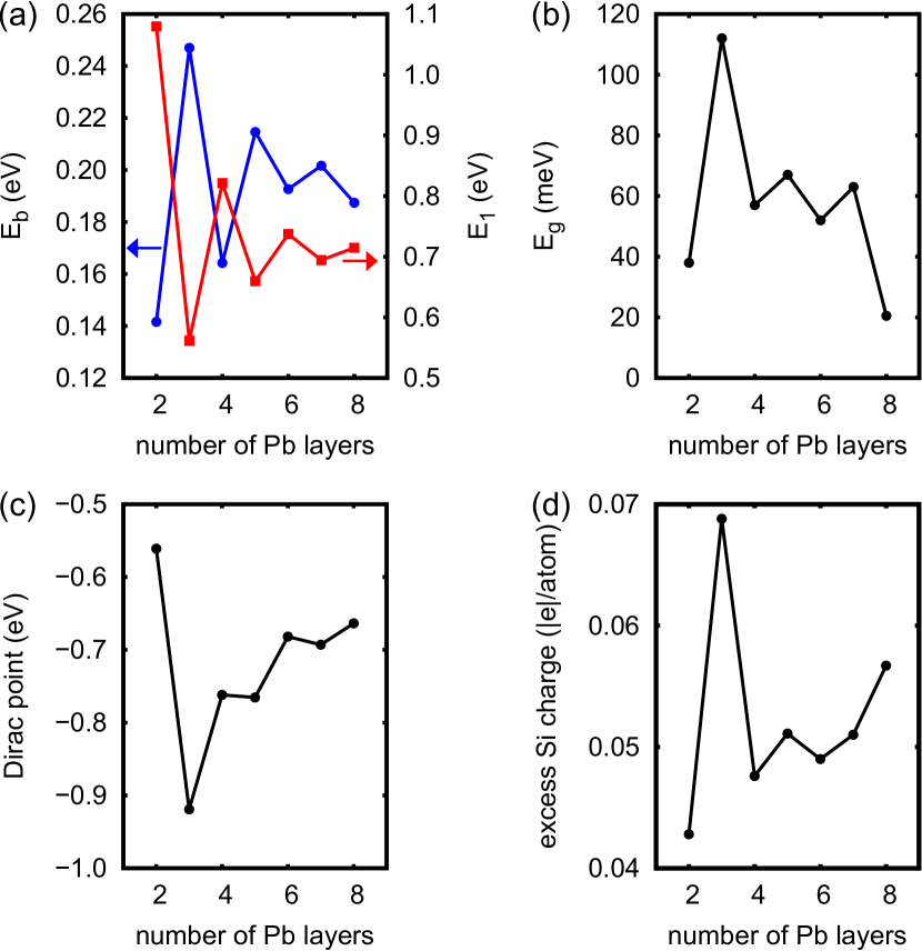
Clear oscillations of as a function of Pb thickness are visible. This is the result of different positions of quantized energy levels of Pb film due to the quantum size effect (see Fig. 1 in Ref. sup ). Obviously, these quantum well states are also responsible for binding energy of the top Pb layer to rest of Pb slab [see red line in Fig. 1 (a)]. Thus both, and , show oscillatory behavior as a function of number of Pb layers, but they oscillate in antiphase. It means that if the top Pb layer is bound strongly (weakly) to rest of the slab, it binds silicene weakly (strongly). This is an example of common wisdom in chemistry on the bonding of atoms, i.e. if a given atom is strongly involved in bonding with one of its neighbors, at the same time it weakens its bonds with the other neighbor Ossowski et al. (2015). Such behavior of the binding energy can be exploited in the growth of silicene layer. Changing the thickness of a slab, thus the binding energy, we modify the growing conditions for silicene. Thus we are equipped with a new tool to control the formation of silicene. The same scenario should be realized in other 2D systems on various thin metal layers, provided van der Waals interactions are not much important, and substrates exhibit QSE. Obviously, this is unlikely to work for graphene.
Surprisingly, the binding energy oscillations are not reflected in substantial changes of the silicene atomic structure. The silicene layer is buckled and consists of Si atoms in their top and bottom positions Podsiadły-Paszkowska and Krawiec (2015). The arrangement of Si atoms is almost the same, independent of QW thickness. The influence of QSE leads only to different mean separations of silicene and Pb surface, with large (small) distance for weak (strong) silicene-substrate interaction, and to small variations of the buckling, only to 0.06 Å. The energy ordering of different silicene reconstructions, predicted in Ref. 29, is not sensitive to QSE either. The lack of structural modifications is supported by recent experiment on silicene on Ag(111) films, albeit containing more atomic layers Sone et al. (2014).
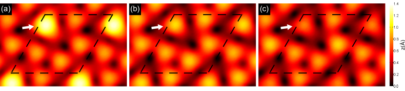
Scanning tunneling microscopy (STM) topography images calculated for silicene on quantum wells of different thickness show, however, noticeable changes, as one can deduce from experiments on bare Pb layers Eom et al. (2006). These changes are most pronounced for Si atoms in the top position, as it is visible in Fig. 2 for marked bright protrusion.
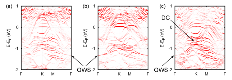
This suggests that electronic effects play an important role in the system. Namely, the QW states of the substrate provoke changes in the electronic structure of silicene, thus influence the STM topography. Indeed, this is clearly visible in Fig. 3, where evolution of the energy bands as a function of Pb thickness is shown.
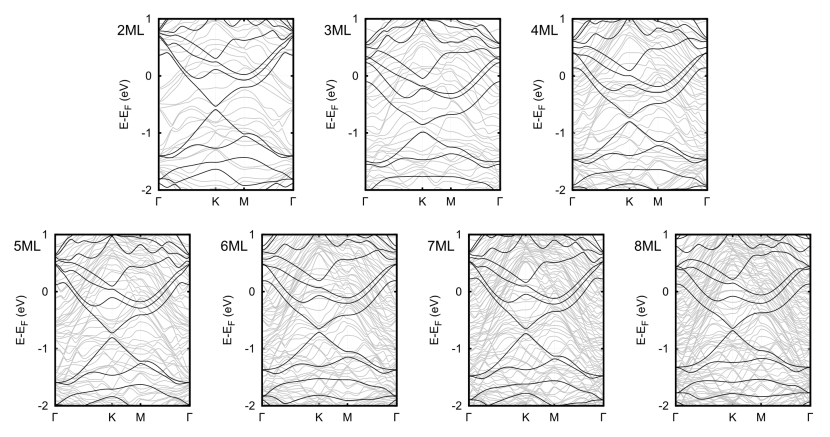
In all cases bands with linear dispersion can be detected, albeit modified. Due to the presence of a substrate, the inversion symmetry of silicene lattice is broken, which results in the opening of an energy gap at the Dirac point. The magnitude of this gap, is related to QSE via the binding energy and the mean silicene-Pb surface separation, and oscillates as a function of QW thickness [see Fig. 1 (b)].
Similarly, position of the Dirac point [Fig. 1 (c)], defined as energy in the middle of the Dirac cone gap, can be shifted by approximately 0.4 eV by varying QW thickness. This effect is accompanied by charge transfer between both subsystems, as it is evidenced in Fig. 1 (d). However, the situation is more complicated, and additional mechanism must be present, since this charge transfer is too low to shift the Dirac point so deep in the valence bands. Indeed, not all Si atoms receive negative charge, as the Bader analysis indicates. Namely, Si atoms in the lower layer, which contribute mainly to the Dirac cone, are doped by electrons from the top Si layer, which further shifts the Dirac cone down. Thus the electron charge is transferred from both Pb and top Si atoms to the bottom Si atoms. Moreover, there is strong hybridization of electron states, mainly derived from p-orbitals of Si ( and bands of silicene) and Pb atoms, in vicinity of the point. This can be observed while comparing unsupported silicene bands with the band structure of the full slab near the point. Clearly, strong modifications of the unsupported silicene bands are visible. Note that the strain imposed on silicene layer is too weak to shift the Dirac cone Wang and Ding (2013).
The charge transfer between top and bottom Si atoms not only shifts the Dirac cone, but is an intrinsic factor of a novel effect, which we call self-protection of silicene. The important role in the mechanism of self-protection falls to the top Si atoms in supported silicene layer. Namely, the electrons of silicene try to avoid the destructive influence of a substrate as much as they can for the price of strong interaction between top Si atoms with Pb film. Such behavior is triggered by the QSE, as the electron wave function forms a standing wave limited by bottom of the slab and the top-most objects (top Si atoms). Thus the role of the top Si atoms is to decouple the Dirac electrons in silicene from other parts of the system. Consequently, we can think of silicene on a substrate as an electron doped quasi-free-standing layer with top Si atoms acting as substitutional impurities. This scenario is supported by projected band structure, shown in Fig. 4.
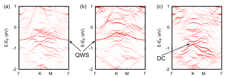
Clearly, the main contribution to the linear bands comes from the bottom Si atoms, with a weak impact of Pb 6pz and even weaker of top Si 3pz states. On the other hand, there is strong interaction between Pb and top Si pz orbitals, forming QW states. This is a hallmark of the self-protection mechanism. Note that there is no trace of this QW state in the electronic structure of the bottom Si atoms. Thus the Dirac cone in silicene on QW survives and the electrons of silicene try to be decoupled from the rest of the system owing to strong interaction between Pb and top Si atoms. We think that the self-protection scenario is realized in other supported 2D systems, like silicene on Ag(111), where the atomic structure of silicene also features a few Si atoms in the unit cell sticking out of the Si layer. However in this case the self-protection mechanism may be too weak to compete with the very strong silicene-substrate interaction.
The decoupling of -electrons depends on relative position of the Dirac point and QW state, and can be slightly suppressed if both coincide, as it is seen in Fig. 5.
This may occasionally happen for certain thicknesses, and rather for thicker films, where the separation between QW states is smaller.
Finally, we would like to discuss the experimental realization of the proposed method of growing and controlling 2D silicene-like systems. The strongest effect should be observed for thin films. However, the QWs also require substrates. Therefore, it is important to chose the substrate on which the film can be grown in a layer by layer mode. Furthermore, present calculations have been performed for unsupported QWs. The underlying substrate on which thin films could be grown will certainly influence the QW states to some extent. Therefore, one can choose a substrate with minor impact on QW states like, for example, single-crystalline epitaxial graphite Dil et al. (2007). On the other hand, the supported quantum wells may even help to control the properties of silicene, as in the case of Pb films on Si(111) surface, where the QW states become less dispersive, and remain flat in a large part of the Brillouin zone Slomski et al. (2011). Thus the silicene properties should be more controllable. Finally, we would like to stress that the proposed idea can be utilized in other 2D materials on various substrates exhibiting QSE.
In conclusion, we proposed a powerful method of controlling the silicene-substrate interaction owing to the quantum size effect. We have demonstrated that the electronic properties of silicene on metallic quantum wells, like binding energy, position of the Dirac cone and magnitude of the energy gap at the Dirac point, can easily be tuned by quantum well states of the substrate. This idea can be utilized in other 2D silicene-like materials growing on various thin films. We also discovered the effect of self-protection of silicene, in which the top Si atoms play a crucial role, taking on the interaction with the substrate, and decoupling Dirac electrons from the rest of the system. These findings emphasize the essential role of interfacial coupling and open new routes to create two-dimesnional structures with tailored electronic properties.
This work has been supported by the National Science Centre under Grant no. 2014/15/B/ST5/04244.
References
- Takeda and Shiraishi (1994) K. Takeda and K. Shiraishi, Phys. Rev. B 50, 14916 (1994).
- Cahangirov et al. (2009) S. Cahangirov, M. Topsakal, E. Aktürk, H. Sahin, and S. Ciraci, Phys. Rev. Lett. 102, 236804 (2009).
- Ni et al. (2012) Z. Ni, Q. Liu, K. Tang, J. Zheng, J. Zhou, R. Qin, Z. Gao, D. Yu, and J. Lu, Nano Lett. 12, 113 (2012).
- Drummond et al. (2012) N. D. Drummond, V. Zolyomi, and V. I. Falko, Phys. Rev. B 85, 075423 (2012).
- Tsai et al. (2013) W. F. Tsai, C. Y. Huang, T. R. Chang, H. Lin, H. T. Jeng, and A. Bansil, Nature Commun. 4, 1500 (2013).
- Osborn et al. (2011) T. H. Osborn, A. A. Farajian, O. V. Pupysheva, R. S. Aga, and L. C. Lew Yan Voon, Chem. Phys. Lett. 511, 101 (2011).
- Lin and Ni (2012) X. Lin and J. Ni, Phys. Rev. B 86, 075440 (2012).
- Zheng and Zhang (2012) F.-B. Zheng and C.-W. Zhang, Nanoscale Res. Lett. 7, 422 (2012).
- Vogt et al. (2012) P. Vogt, P. De Padova, C. Quaresima, J. Avila, E. Frantzeskakis, M. C. Asensio, A. Resta, B. Ealet, and G. Le Lay, Phys. Rev. Lett. 108, 155501 (2012).
- Fleurence et al. (2012) A. Fleurence, R. Friedlein, T. Ozaki, H. Kawai, Y. Wang, and Y. Yamada-Takamura, Phys. Rev. Lett. 108, 245501 (2012).
- Meng et al. (2013) L. Meng, Y. Wang, L. Zhang, S. Du, R. Wu, L. Li, Y. Zhang, G. Li, H. Zhou, W. A. Hofer, et al., Nano Lett. 13, 685 (2013).
- Morishita et al. (2013) T. Morishita, M. J. S. Spencer, S. Kawamoto, and I. K. Snook, J. Phys. Chem. C 117, 22142 (2013).
- Aizawa et al. (2014) T. Aizawa, S. Suehara, and S. Otani, J. Phys. Chem. C 118, 23049 (2014).
- Jamgotchian et al. (2012) H. Jamgotchian, Y. Colington, N. Hamazaouri, B. Ealet, J. Hoarau, B. Aufray, and J. P. Biberian, J. Phys.: Condens. Matter 24, 172001 (2012).
- Chiappe et al. (2012) D. Chiappe, C. Granzietti, G. Tallarida, M. Fanciulli, and A. Molle, Adv. Matter 24, 5088 (2012).
- Majzik et al. (2013) Z. Majzik, M. R. Tchalala, M. Svec, P. Hapala, H. Enriquez, A. Kara, A. J. Mayne, G. Dujardin, P. Jelinek, and H. Oughaddou, J. Phys.: Condens. Matter 25, 225301 (2013).
- Chen et al. (2012) L. Chen, C. C. Liu, B. Feng, X. He, P. Cheng, Z. Ding, S. Meng, Z. G. Zao, and K. H. Wu, Phys. Rev. Lett. 109, 056804 (2012).
- Wang and Cheng (2013) Y. Wang and H. Cheng, Phys. Rev. B 87, 245430 (2013).
- Guo et al. (2013) Z. Guo, S. Furuya, J. I. Iwata, and A. Oshiyama, Phys. Rev. B 87, 235435 (2013).
- Lin et al. (2013) C. Lin, R. Arafune, K. Kawahara, M. Kanno, N. Tsukahara, E. Minamitani, Y. Kim, M. Kawai, and N. Takagi, Phys. Rev. Lett. 110, 076801 (2013).
- Feng et al. (2013) B. Feng, H. Li, C. Liu, T. Shao, P. Cheng, Y. Yao, S. Meng, L. Chen, and K. Wu, ACS Nano 10, 9049 (2013).
- Feng et al. (2015) Y. Feng, D. Liu, B. Feng, X. Liu, L. Zhao, Z. Xie, Y. Liu, A. Liang, C. Hu, Y. Hu, et al., arXiv:1503.06278 (2015).
- Liu et al. (2013) H. Liu, J. Gao, and J.Zhao, J. Phys. Chem. C 117, 10353 (2013).
- Bhattacharya et al. (2013) A. Bhattacharya, S. Bhattacharya, and G. P. Das, Appl. Phys. Lett. 103, 123113 (2013).
- Zhu and Schwingenschlögl (2014) J. Zhu and U. Schwingenschlögl, Appl. Mater. Interfaces 6, 11675 (2014).
- Gao et al. (2014) N. Gao, J. C. Li, and Q. Jiang, Chem. Phys. Lett. 592, 222 (2014).
- Kokott et al. (2014) S. Kokott, P. Pflugradt, L. Matthes, and F. Bechstedt, J. Phys.: Condens. Matter 26, 185002 (2014).
- Pflugradt et al. (2014) P. Pflugradt, L. Matthes, and F. Bechstedt, New J. Phys. 16, 075004 (2014).
- Podsiadły-Paszkowska and Krawiec (2015) A. Podsiadły-Paszkowska and M. Krawiec, Phys. Chem. Chem. Phys. 17, 2246 (2015).
- Schulte (1976) F. K. Schulte, Surf. Sci. 55, 427 (1976).
- Jałochowski et al. (1992) M. Jałochowski, H. Knoppe, G. Lilienkamp, and E. Bauer, Phys. Rev. B 46, 4693 (1992).
- Materzanini et al. (2001) G. Materzanini, P. Saalfrank, and P. Lindan, Phys. Rev. B 63, 235405 (2001).
- Tringides et al. (2007) M. C. Tringides, M. Jałochowski, and E. Bauer, Phys. Today 60, 50 (2007).
- Dil et al. (2007) J. H. Dil, B. Hülsen, T. Seyller, and K. Horn, Phys. Rev. B 75, 161401 (2007).
- Slomski et al. (2011) B. Slomski, F. Meier, J. Osterwalder, and J. H. Dil, Phys. Rev. B 83, 035409 (2011).
- Ordejon et al. (1996) P. Ordejon, E. Artacho, and J. Soler, Phys. Rev. B 53, 10441 (1996).
- Sánchez-Portal et al. (1997) D. Sánchez-Portal, P. Ordejón, E. Artacho, and J. Soler, Int. J. Quantum Chem. 65, 453 (1997).
- Artacho et al. (1999) E. Artacho, D. Sánchez-Portal, P. Ordejón, A. García, and J. Soler, Phys. Status Solidi B 215, 809 (1999).
- Soler et al. (2002) J. Soler, E. Artacho, J. Gale, A. García, J. Junquera, P. Ordejón, and D. Sánchez-Portal, J. Phys.: Condens. Matter 14, 2745 (2002).
- Artacho et al. (2008) E. Artacho, E. Anglada, O. Dieguez, J. D. Gale, A. García, J. Junquera, R. M. Martin, P. Ordejón, J. M. Pruneda, D. Sánchez-Portal, et al., J. Phys.: Condens. Matter 20, 064208 (2008).
- Perdew et al. (1996) J. P. Perdew, K. Burke, and M. Ernzerhof, Phys. Rev. Lett. 77, 3865 (1996).
- Troullier and Martins (1991) N. Troullier and J. L. Martins, Phys. Rev. B: Condens. Matter 43, 1993 (1991).
- Monkhorst and Pack (1976) H. J. Monkhorst and J. D. Pack, Phys. Rev. B 13, 5188 (1976).
- Tersoff and Hamann (1983) J. Tersoff and D. R. Hamann, Phys. Rev. Lett. 50, 1998 (1983).
- Tersoff and Hamann (1985) J. Tersoff and D. R. Hamann, Phys. Rev. B 31, 805 (1985).
- Bader (1990) R. F. W. Bader, Atoms in Molecules – a quantum theory (Oxford University Press, New York, 1990).
- (47) See Supplemental Material at http://link.aps.org/supplemental.
- Ossowski et al. (2015) J. Ossowski, J. Rysz, M. Krawiec, D. Maciazek, Z. Postawa, A. Terfort, and P. Cyganik, Angew. Chem. Int. Ed. 54, 1336 (2015).
- Sone et al. (2014) J. Sone, T. Yamagami, Y. Aoki, K. Nakatsuji, and H. Hirayama, New J. Phys. 16, 095004 (2014).
- Eom et al. (2006) D. Eom, S. Qin, M.-Y. Chou, and C. K. Shih, Phys. Rev. Lett. 96, 027005 (2006).
- Wang and Ding (2013) Y. Wang and Y. Ding, Solid State Commun. 155, 6 (2013).