Electron-induced limitation of surface plasmon propagation in silver nanowires
Abstract
Plasmonic circuitry is considered as a promising solution-effective technology for miniaturizing and integrating the next generation of optical nano-devices. A key element is the shared metal network between electrical and optical information enabling an efficient hetero-integration of an electronic control layer and a plasmonic data link. Here, we investigate to what extend surface plasmons and current-carrying electrons interfere in such a shared circuitry. By synchronously recording surface plasmon propagation and electrical output characteristics of single chemically-synthesized silver nanowires we determine the limiting factors hindering the co-propagation of electrical current and surface plasmons in these nanoscale circuits.
pacs:
73.20.Mf, 81.07.Gf, 66.30.Qa1 Introduction
Plasmonic circuitry [1, 2] is a unique platform capable for simultaneously sustaining an optical signal encoded in the form of a surface plasmon and an electrical current. This emerging technology has attracted tremendous interest for its potential to interface electronics and photonics at the nanoscale [3, 4, 5, 6, 7]. The ability to guide surface plasmons and electrons on the same physical link may enable a seamless integration of an optical data processing level within an electronic control architecture [8, 9, 10].
Among the variety of plasmonic waveguides developed to date [11, 12, 13, 14, 15], quasi-one dimensional structures like silver and gold nanowires are especially desirable because they have potential for realizing dense plasmonic and electronic routing networks. In particular, chemically-synthesized metal nanowires offer a unique medium to guide and manipulate surface plasmon at the nanoscale with improved performances [16, 17, 18, 19]. Surface plasmon modes can be readily excited in these structures by different coupling strategies [16, 20, 21, 22, 23] and signal-processing functionalities were recently demonstrated including routing [24, 25, 26], logic functions [27], modulation [28] and plasmon electrical detection [29]. Despite an advanced control of the surface plasmon field, integration of the platform with an electronic layer has remained elusive and confined to a thermo-optical activation of dielectric-loaded surface plasmon stripe waveguides [30, 31]. For metal nanowires, it is not clear to which extent surface plasmon characteristics are retained under direct-current (DC) biasing operation. This question is however critical to assess the capability of a plasmonic circuitry to simultaneously sustain surface plasmon propagation and an electrical current.
In this paper, we investigate the effect of an electron flow on the surface plasmon properties when these two information channels are transported synchronously in chemically-synthesized metal nanowires. By recording surface plasmon characteristics as a function of the electrical environment, limiting factors affecting the co-propagation are experimentally determined.
2 Electrical characterization
Pentagonal-twinned silver nanowires were synthesized using a modified polyol process producing nanowires with section width comprised between 300 nm and 600 nm [32]. The colloidal solution of nanowires was then drop-casted on a glass substrate pre-patterned with grid landmarks to precisely coordinate the position of selected nanowires. Electrical contacts were designed by electron-beam lithography to connect the extremities of individual nanowires. A 70 nm-thick gold layer was evaporated to form the conductive leads. Because the thickness of the electrodes was smaller than the radius of the nanowires, Au evaporation was performed at a azimutal angle to insure electrical continuity between the electrodes and the nanowire. The structures were electrically biased by a regulated low voltage power supply and current flow was recorded with a home-made current-to-voltage converter in a two-point configuration.
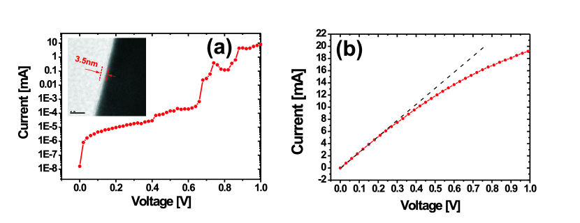
A representative electrical output characteristic of a contacted Ag nanowire is displayed in semi-logarithmic scale in Fig. 1(a) during an initial bias sweep. Current flowing in the nanowire is typically low across a large range of bias and occurs by increasing steps. This non-ohmic current/voltage behavior of the nanowire originates from the initially poor electrical connection between the nanowire and the leads. The chemistry employed to synthesize the nanowires uses an excess of polyvinylpyrrolidone (PVP) surfactant that is bound to the surface of the nanowire. A transmission electron micrograph (TEM) showing a 3.5 nm thick surfactant layer is displayed in the inset of Fig. 1(a). This organic layer acts as a dielectric tunnel barrier preventing current to flow between the electrodes and the nanowire. Irregularity in the current/voltage characteristic occurs at current densities that are large enough to physically destroy the surfactant layer. For current above 5 to 10 mA, the typical resistance is below 100 indicating a metallic electrical contact. This is demonstrated in Fig. 1(b) where the current/voltage characteristic was measured again during a subsequent bias sweep following the initial run. A monotonous rise of the current with increasing voltage is observed. For low voltage, the current/voltage characteristic follows a linear trend (dashed curve) with a slope of 25 corresponding to the total resistance of the contacts. The resistance of the contacts between the probes and electrodes was measured by contacting the two probes close to each other (separation distance the length of the nanowire) on the same electrode. A real resistance of the Ag nanowire at around 2.35 was thus determined yielding a resistivity =1.55 .cm according to , where is the subtracted resistance, is the cross-sectional area of the silver nanowire, and is its longitudinal length. This resistivity is very close to the standardized bulk value of silver 1.59 .cm at room temperature [33]. After 0.3 V, the trend becomes nonlinear with an increasing resistance of the nanowire with voltage. This variation of resistance is due to the temperature rise caused by the current flow [34] and the onset of morphological changes induced by an electromigration process [35, 36, 37]. The effect of surfactant on the electron flow and the subsequent monotonous current/voltage characteristics showed in Fig. 1(a) and (b) were systematically measured for all contacted Ag nanowires. The current/voltage characteristic displayed in Fig. 1(b) is reproducible if the current flowing through the nanowire is kept below the density required to initiate the electromigration of Ag atoms. For voltage sweeps typically exceeding 1V, the subsequent on-start resistance increases as a result of electromigration-induced amorphization of the nanowire.
3 Surface plasmon analysis
We now turn our attention to the properties of surface plasmons propagating in these electrically-biased nanowires. Surface plasmons were launched by using an oil immersion objective. A laser emitting at 800 nm was focused on a diffraction-limited spot at one end of a contacted nanowire. Scattering at the other end of the nanowire and leakage radiation during surface plasmon propagation were collected by the same objective [38]. Two charge-coupled device (CCD) cameras placed at the conjugated image and Fourier planes of the microscope were used to record the intensity distribution in direct and reciprocal space, respectively [39]. Measurements in the image plane provide a direct visualization of plasmon propagation in the nanowire while parameters like effective index of the guided surface plasmon mode and overall losses were estimated from Fourier plane analysis. Thicker nanowires were preferentially studied in this work rather than nanowires with smaller sections since plasmon detection by leakage radiation microscopy requires energy to leak into the substrate [38]. Leakages only occur above a minimal value of the section set by the local environment [40].
Figure 2(a) displays a typical surface plasmon intensity distribution recorded in the image plane for a contacted Ag nanowire (section width 500 nm) excited with a linear polarization oriented along the propagation. The electrodes are visible in this image. The excitation spot overlapping the lower extremity of the nanowire defines the origin of the reference Cartesian frame (), where is aligned with the long axis of the nanowire. The surface plasmon mode is readily excited in this configuration [41] and leakages radiated during its propagation are observed in the form of luminous lines on both sides of the nanowire [42, 38]. At the distal end, the surface plasmon is scattered out of the waveguide.
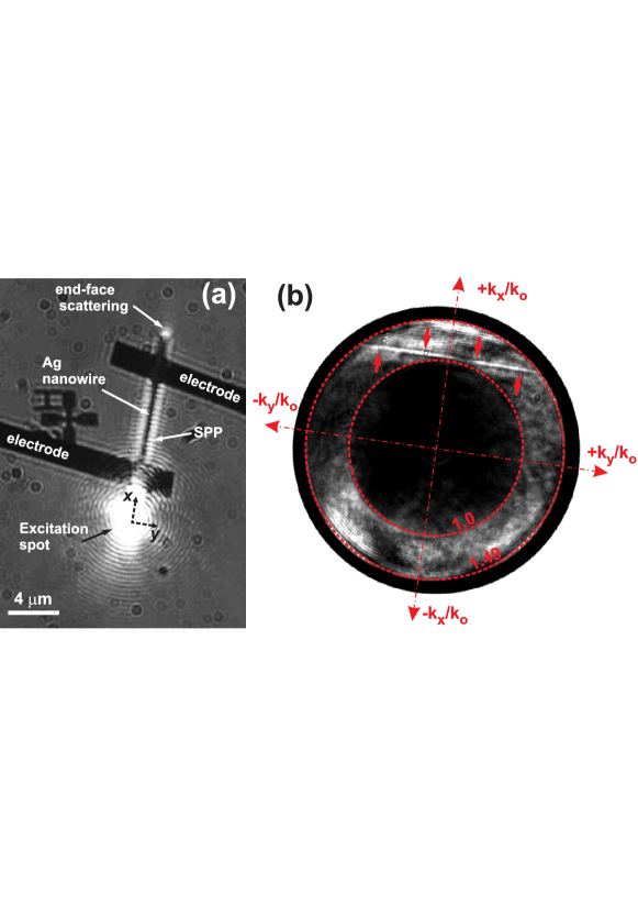
From Fig. 2(a), there is no evidence that the plasmon propagating along the uncoated sections of the wire is significantly altered by the presence of the two 2-m-wide electrodes. At the electrode positions, the field distribution of the mode is modified by the additional 70 nm-thick gold layer on top of the Ag nanowire and no longer leaks in the substrate. However, leakages resume on the uncoated sections indicating that the mode is retained along the pristine nanowire. We hypothesized that a significant field overlap exists between the modes sustained at the electrode-coated sections and the uncovered sections of the nanowire thus promoting energy transfer between the modes [43, 44]. This is equivalent to a hybrid coupling strategies discussed in Ref. [45]. A Fourier image of the wavevector distribution is displayed in Fig. 2(b). The leaky surface plasmon mode is recognized as the unique bright line at an effective index =1.056 (arrows), where is the reciprocal axis and is the free-space wavevector. The outer boundary in Fig. 2(b) indicates the collection limit due to the objective numerical aperture =1.49. The inner boundary corresponds to critical angle of the glass/air interface at =1.0. The extension of the surface plasmon signature along the reflects the lateral confinement of the mode on the nanowire. The imaginary part of the complex effective index is accounted by the width of the line and the measured value at half-maximum =0.09 is comparable to uncontacted nanowires [38]. Efficient scattering of the plasmon mode at the distal end to free-space photons is typical for nanowires with a section greater than 300 nm [46]. Consequently, we did not observed a symmetric line at =-1.056 which would suggest a reflected surface plasmon mode by the end face.
4 Simultaneous plasmon and electron transport
Surface plasmon propagation was simultaneously recorded in this dual-plane imaging mode while synchronously sweeping the DC bias at 30 mV steps. For each voltage/current values, a direct space image and its corresponding Fourier content were recorded. We have then extracted the value of the real and imaginary part of the effective index for each biasing step. The results are reported in Fig. 3(a).
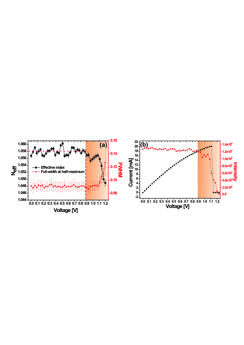
The characteristics of the mode remain almost constant within experimental measurement errors at =1.056+i0.09 until 0.9 V. The dotted line shows the average value of in the [0;0.9 V] voltage range. In this biasing regime, propagation of the leaky plasmon mode is not affected by the flow of charges and the temperature rise of the nanowire. Above 0.9 V (shaded areas), drops below the average value and both the real and imaginary part of the complex effective index become dependent on the biasing condition. Extrinsic propagation losses encoded in the rise of are concomitant to a measurable reduction of . After 1.2 V, there is no longer any evidence of a plasmon signature in the Fourier plane. The rise of propagation loss after 0.9 V is confirmed by the rapid drop of the scattered intensity with voltage measured at the distal end of the nanowire as shown by the red curve (circle) in Fig. 3(b).
The change of the effective index and propagation loss is closely related to the electrical output characteristic of the nanowire reported again in Fig. 3(b). The plasmon propagation is affected by the applied bias at the point where electromigration of the nanowire becomes predominant in the current/voltage characteristic (shaded area). The largest variation of and occurs when the current suddenly drops indicating electrical breakdown of the nanowire. Under such electrical stress, the morphology of the nanowire is significantly affected [47] thus compromising plasmon propagation.
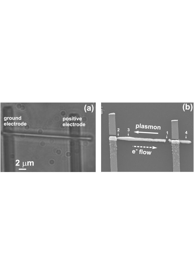
To confirm this drastic morphological change, we have imaged the nanowires before applying a bias and after electrical breakdown. Freshly contacted nanowires were observed by bright-field optical microscopy in order to avoid electron-beam carbon contamination by a scanning electron microscope (SEM). After electromigration however, a thin layer of Au (20 nm) was sputtered on the sample for a detailed SEM investigation. Representative images of a 18 m-long 500 nm-wide Ag nanowire before and after electromigration are shown in Fig. 4(a) and (b), respectively. The SEM image obtained after electromigrating the nanowire confirms the structural deformation. For all investigated Ag nanowires, electrical failure occurs at the positive electrode (point 1). This behavior, already reported for another type of crystalline Ag nanowires [48, 49], suggests that the breakage originates from a motion of charged atoms initiated by the electric field present across the nanowire. However, Fig. 4(b) also shows a weaker but visible mass transport along the electron flow: a thinner nanowire section near the ground electrode (point 2) is visible in the SEM image. This section is immediately followed by a wider area (point 3) indicating that Ag atoms were displaced from point 2 to point 3. The original nanowire section is measured at point 4, on the right of the positive electrode. At this location, the electron flow did not affect the nanowire. Note that the section at point 3 is wider than the original nanowire size at point 4. We have also switched the biasing polarity, i.e. electrons and plasmon propagating in the same direction. We did not observe significant differences from the trend displayed in Fig. 3(a).
5 Numerical determination of the surface plasmon effective index
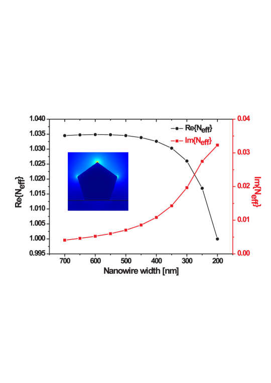
From Fig. 4(b) it is clear that the evolution of the surface plasmon effective index and propagation loss with applied bias described in Fig. 3(a) can be attributed to the altered section of the nanowire and loss of crystallinity caused by the electromigration process. To test this hypothesis, we numerically investigated the effect of a varying nanowire section on the effective index and propagation loss of the surface plasmon using the finite-element analysis simulation software COMSOL Multiphysics. We considered an infinitely long pentagonal silver nanowire on a glass substrate with an excitation wavelength nm and a silver optical index . Since the effective index of the leaky plasmon mode is very close to 1.0, the mode is significantly extending in the air medium. To account for this, we add perfectly-matched layers on the air side of the calculation window. The evolution of the effective index with reducing nanowire section is reported in Fig. 5; the cross-sectional intensity distribution of the mode is displayed in the inset for a section of 300 nm. The and are weakly depending on nanowire section until approximatively 450 nm. For width nm, monotonously decreases towards the cutoff value of the mode (1.0), a condition confirmed by the associated larger losses in this section range. A small discrepancy between the experimental and calculated can be attributed to the dielectric constant used, the presence of the PVP polymer on the surface of the nanowire, and experimental errors in calibrating Fourier planes. A larger discrepancy is however present for the . For a 500 nm-wide nanowire, we experimentally measured =0.09 while the calculation indicates a value approaching 0.01. Residual roughness present along the chemically-synthesized Ag nanowire is probably contributing to the widening of the Fourier signature of the surface plasmon mode. We showed in Ref. [38] that the finite length of the nanowire is affecting . End-face scattering introduces an additional decay channel contributing to the total loss experienced by the leaky surface plasmon mode.
According to SEM images of electromigrated nanowires, the thinnest unbroken section is around 250 nm to 300 nm. The calculated dispersion curve shows that the of the mode is reduced from 1.034 to , a change of 0.014 in this section range. Although the relationship between the width of the nanowire and the applied bias is not trivial (non linear electrical characteristic and local variations along the length), the measured difference of before and after breakdown in Fig. 3(a) (0.010) is comparable to our numerical simulations. Concerning the imaginary part , the calculation also qualitatively reproduces the experimental trend of Fig. 3(a). Amorphization of the chemically-synthesized nanowire during the electromigration process and variation of the section along the nanowire length were omitted in the calculation. Both effects introduce additional plasmon damping compared to pristine nanowires [17] and accounts for the under approximation of the plasmon losses in Fig. 5.
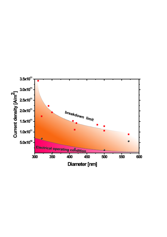
From the above investigations, change in the morphology of the nanowire appears to be the main limitation for co-propagating plasmonic and electronic information in metal nanowires. Figure 6 shows the maximum current densities before electrical failure (red squares) as a function of nanowire section. Like Cu and Au nanowires, the failure current density in crystalline Ag structures depends on the section as a results of a better heat dissipation in the glass substrate [34, 35, 50]. The data points represented with black circles are the measured current densities after which the corresponding of the surface plasmon mode drops below the average value measured at low voltage bias (see Fig. 3(a)). This boundary is therefore an upper limit on the the electrical condition under which electron and (leaky) surface plasmon can be simultaneously supported by the plasmonic platform. The red-shaded area beneath these data points represents the safe electrical operation. In the orange area located between the two curves, electron-induced degradation of the surface plasmon mode is occurring. Thin nanowires can sustain a higher current density and, from an electrical point of view, should be favored in the circuitry. However, surface plasmons in thin nanowires are tightly bound modes and are thus expected to be more sensitive to subtle change occurring at the nanowire surface. We hope to provide experimental evidence for that in a follow-up communication.
In summary, we have investigated the effect of electron flow on plasmon propagation in electrically contacted chemically-synthesized silver nanowires. We find that surface plasmon characteristics are degraded by the morphological stress of the nanowire caused at the onset of electromigration. We have thus determined the operating limit for simultaneously propagating electrons and surface plasmon in the same one-dimensional metallic support, a prerequisite for realizing a practical plasmonic circuitry interfacing integrated photonic and electronic devices.
References
References
- [1] E. Ozbay. Plasmonics: merging photonics and electronics at nanoscale dimensions Science 311:189, 2006
- [2] Th. W. Ebbesen, C. Genet, and S. I. Bozhevolnyi. Surface–plasmon circuitry. Phys. Today, 61(5):44–50, 2008.
- [3] W. L. Barnes, A. Dereux, and Th. W. Ebbesen. Surface plasmon subwavelength optics. J. Nature., 424(14):824–830, 2003.
- [4] H. A. Atwater. The promise of plasmonics. Sci. Am., 296(4):56–62, 2007.
- [5] D. K. Gramotnev and S. I. Bozhevolnyi. Plasmonics beyond the diffraction limit. Nat. Photonics., 4(2):83–91, 2010.
- [6] M. Dragoman and D. Dragoman. Plasmonics : applications to nanoscale terahertz and optical devices. Prog. Quant. Electr., 32(1):1–41, 2008.
- [7] J. A. Schuller, E. S. Barnard, W. Cai, Y. C. Jun, J. S. White, and M. L. Brongersma. Plasmonics for extreme light concentration and manipulation. Nature Mat., 9(3):193–204, 2010.
- [8] R. Zia, J. A. Schuller, and M. L. Brongersma. Near-field characterization of guided polariton propagation and cutoff in surface plasmon waveguides. Phys. Rev. B, 74:165415, 2006.
- [9] J. J. Ju, S. Park, M.-S. Kim, J. T. Kim, S. K. Park, and Y. J. Park. 40 Gbit / s light signal transmission in long-range surface plasmon waveguides. Appl. Phys. Lett., 91(17):171117, 2007.
- [10] P. Neutens, P. Van Dorpe, I. De Vlaminck, L. Lagae, and G. Borghs. Electrical detection of confined gap plasmons in metal/insulator/metal waveguides. Nature Phot., 3(5):283–286, 2009.
- [11] J.-C. Weeber, A. Dereux, Ch. Girard, J. R. Krenn, and J.-P. Goudonnet. Plasmon polaritons of metallic nanowires for controlling submicron propagation of light. Phys. Rev. B, 60(12):9061–9068, 1999.
- [12] J. Grandidier, G. Colas des Francs, L. Markey, A. Bouhelier, S. Massenot, J.-C. Weeber, and A. Dereux. Dielectric-loaded surface plasmon polariton waveguides on a finite-width metal strip. Appl. Phys. Lett., 96(6):063105, 2010.
- [13] S. A. Maier, M. L. Brongersma, P. G. Kik, S. Meltzer, A. A. G. Requicha, and H. A. Atwater. Plasmonics-a route to nanoscale optical devices. Adv. Mater., 13(19):1501–1505, 2001.
- [14] L. Liu, Z. Han, and S. He. Novel surface plasmon waveguide for high integration. Opt. Express., 13(17):6645–6650, 2005.
- [15] Y. Fedutik, V. V. Temnov, O. Schöps, and U. Woggon. Exciton-plasmon-photon conversion in plasmonic nanostructures. Phys. Rev. Lett., 99(13):136802, 2007.
- [16] R. M. Dickson and L. A. Lyon. Unidirectional plasmon propagation in metallic nanowires. J. Phys. Chem. B, 104(26):6095–6098, 2000.
- [17] H. Ditlbacher, A. Hohenau, D. Wagner, U. Kreibig, M. Rogers, F. Hofer, F.R. Aussenegg, and J.R. Krenn. Silver nanowires as surface plasmon resonators. Phys. Rev. Lett., 95(25):257403, 2005.
- [18] M. W. Knight, N. K. Grady, R. Bardhan, F. Hao, P. Nordlander, and N. J. Halas. Nanoparticle-mediated coupling of light into a nanowire. Nano Lett., 7(8):2346–2350, 2007.
- [19] J. A. Conway, S. Sahni, and Th. Szkopek. Plasmonic interconnects versus conventional interconnects: a comparison of latency, crosstalk and energy costs. Opt. Express, 15(8):4474–4484, 2007.
- [20] D. J. Sirbuly, M. Law, P. Pauzauskie, H. Yan, A.V. Maslov, K. Knutsen, C.Z. Ning, R.J. Saykally, and P. Yang. Optical routing and sensing with nanowire assemblies. Proc. Nat. Acad. Sci., 102(22):7800, 2005.
- [21] A. L. Pyayt, B. Wiley, Y. Xia, A. Chen, and L. Dalton. Integration of photonic and silver nanowire plasmonic waveguides. Nature Nanotech., 3(5):660–665, 2008.
- [22] R. Yan, P. Pausauskie, J. Huang, and P. Yang. Direct photonic-plasmonic coupling and routing in single nanowires. Proc. Nat. Acad. Sci., 106(50):21045–21050, 2009.
- [23] Z. Fang, L. Fan, C. Lin, D. Zhang, A. J. Meixner, and X. Zhu. Plasmonic coupling of bow tie antennas with Ag nanowire. Nano Lett., 11(4):1676–1680, 2011.
- [24] A. Manjavacas and F. J. García de Abajo. Robust plasmon waveguides in strongly interacting nanowire arrays. Nano Lett., 9(4):1285–1289, 2009.
- [25] Y. Fang, Z. Li, Y. Huang, S. Zhang, P. Nordlander, N. J. Halas, and H. Xu. Branched silver nanowires as controllable plasmon routers. Nano Lett., 10(5):1950–1954, 2010.
- [26] Q. Li, S. Wang, Y. Chen, M. Yan, L. Tong, and M. Qiu. Experimental demonstration of plasmon propagation, coupling, and splitting in silver nanowire at 1550-nm wavelength. IEEE, 17(4):1107–1111, 2011.
- [27] H. Wei, Z. Li, X. Tian, Z. Wang, F. Cong, N. Liu, S. Zhang, P. Nordlander, N. J. Halas, and H. Xu. Quantum dot-based local field imaging reveals plasmon-based interferometric logic in silver nanowire networks. Nano Lett., 11(2):471–475, 2011.
- [28] Z. Li, S. Zhang, N. J. Halas, P. Nordlander, and H. Xu. Coherent modulation of propagating plasmons in silver-nanowire-based structures. Small, 7(5):593–596, 2011.
- [29] A. L. Falk, F. H. L. Koppens, C. L. Yu, K. Kang, N. de Leon, Snapp, A. V. Akimov, and M. D. Lukin, M.-H. Jo, and H. Park. Near-field electrical detection of optical plasmons and single-plasmon sources. Nature Phys., 5(7):475–479, 2009.
- [30] K. Leosson, T. Nikolajsen, A. Boltasseva, and S. I. Bozhevolnyi. Long-range surface plasmon polariton nanowire waveguides for device applications. Opt. Express, 14(1):314–319, 2006.
- [31] J. Gosciniak, S. I. Bozhevolnyi, T. B. Andersen, V. S. Volkov, J. Kjelstrup-Hansen, L. Markey, and A. Dereux. Thermo-optic control of dielectric-loaded plasmonic waveguide components. Opt. Express, 18(2):1207–1216, 2010.
- [32] C.-X. Kan, J.-J. Zhu, and X.-G. Zhu. Silver nanostructures with well-controlled shapes: synthesis, characterization and growth mechanisms. J.Phy. D: Appl. Phys., 41(15):155304, 2008.
- [33] Y. Peng, T. Cullis, and B. Inkson. Accurate electrical testing of individual gold nanowires by in situ scanning electron microscope nanomanipulators. Appl. Phys. Lett., 93:183112, 2008.
- [34] C. Durkan and M. E. Welland. Analysis of failure mechanisms in electrically stressed gold nanowires. Ultramicro., 82(1):125–133, 2000.
- [35] Q. Huang, C. M. Lilley, R. Divan, and M. Bode. Electrical failure analysis of au nanowires. Nanotech., IEEE Trans. on, 7(6):688–692, 2008.
- [36] B. Stahlmecke and G. Dumpich. Resistance behaviour and morphological changes during electromigration in gold wires. Phys. Condens. Matter., 19:046210, 2007.
- [37] R. Hoffmann, D. Weissenberger, J. Hawecker, and D. Stöffler. Conductance of gold nanojunctions thinned by electromigration. Appl. Phys. Lett., 93(4):043118, 2008.
- [38] M. Song, A. Bouhelier, P. Bramant, J. Sharma, E. Dujardin, D. Zhang, and G. Colas des Francs. Imaging symmetry-selected corner plasmon modes in penta-twinned crystalline Ag nanowires. ACS Nano, 5(7):5874–5880, 2011.
- [39] S. Massenot, J. Grandidier, A. Bouhelier, G. Colas Des Francs, L. Markey, J.-C. Weeber, A. Dereux, J. Renger, M.U. Gonzàlez, and R. Quidant. Polymer metal waveguides characterization by Fourier plane leakage radiation microscopy. Appl. Phys. Lett., 91(24):243102–243102, 2007.
- [40] C.-L. Zou, F.-W. Sun, Y.-F. Xiao, C.-H. Dong, X.-D. Chen, J.-M. Cui, Q. Gong, Z.-F. Han, and G.-C. Guo. Plasmon modes of silver nanowire on a silica substrate. Appl. Phys. Lett., 97(18):183102, 2010.
- [41] T. Laroche and C. Girard. Near-field optical properties of single plasmonic nanowires. Appl. Phys. Lett., 89:233119, 2006.
- [42] Y. Fang, H. Wei, F. Hao, P. Nordlander, and H. Xu. Remote-Excitation Surface-Enhanced Raman Scattering Using Propagating Ag Nanowire Plasmons Nano Lett., 9:2049–2053, 2009.
- [43] J. Seidel, S. Grafström, L. Eng, and L. Bischoff. Surface plasmon transmission across narrow grooves in thin silver films. Appl. Phys. Lett., 82(9):1368–1370, 2003.
- [44] J. Seidel, F. I. Baida, L. Bischoff, B. Guizal, S. Grafström, D. Van Labeke, and L. M. Eng. Coupling between surface plasmon modes on metal films. Phys. Rev. B, 69:121405, 2004.
- [45] X. Guo, M. Qiu, J. Bao, B. J. Wiley, Q. Yang, X. Zhang, Y. Ma, H. Yu, and L. Tong. Direct coupling of plasmonic and photonic nanowires for hybrid nanophotonic components and circuits. Nano Lett., 9(12):4515–4519, 2009.
- [46] V. D. Miljković, T. Shegai, P. Johansson, and M. Käll. Simulating light scattering from supported plasmonic nanowires. Opt. Express, 20(10):10816–10826, 2012.
- [47] P. Xu, S.-H. Jeon, H.-T. Chen, H. Luo, G. Zou, Q. Jia, M. Anghel, C. Teuscher, D. J. Williams, B. Zhang, X. Han, and H.-L. Wang. Facile synthesis and electrical properties of silver wires through chemical reduction by polyaniline. J. Phys. Chem. C, 114:22147–22154, 2010.
- [48] B. Stahlmecke, F.-J. Meyer zu Heringdorf, L. I. Chelaru, M. Horn-von Hoegen, and G. Dumpich. Electromigration in self-organized single-crystalline silver nanowires. Appl. Phys. Lett., 88(5):053122, 2006.
- [49] M. R. Kaspers, A. M. Bernhart, F. J. M. zu Heringdorf, G. Dumpich, and R. Möller. Electromigration and potentiometry measurements of single-crystalline ag nanowires under uhv conditions. J. Phys. Cond. Mat., 21:265601, 2009.
- [50] Q. Huang, C. M. Lilley, M. Bode, and R. Divan. Surface and size effects on the electrical properties of Cu nanowires. J. Appl. Phys., 104(2):023709–023709, 2008.