Compound surface-plasmon-polariton waves guided by a thin metal
layer sandwiched between a homogeneous isotropic dielectric
material and a structurally chiral material
Francesco Chiadini1, Vincenzo Fiumara2, Antonio Scaglione2, Akhlesh Lakhtakia3
1Department of Industrial Engineering, University of Salerno,
via Giovanni Paolo II, 132 - Fisciano (SA), 84084, ITALY
e-mail: fchiadini@unisa.it, ascaglione@unisa.it
2School of Engineering, University of Basilicata,
Viale dell’Ateneo Lucano 10, 85100 Potenza, ITALY
email: vfiumara@unibas.it
3Department of Engineering Science and Mechanics, Pennsylvania State University,
University Park, PA 16802–6812, USA
e-mail: akhlesh@psu.edu
Keywords: compound surface wave, metal, structurally chiral material, surface-plasmon-polariton wave
Abstract
Multiple compound surface plasmon-polariton (SPP) waves can be guided by a structure consisting of a sufficiently thick layer of metal sandwiched between a homogeneous isotropic dielectric (HID) material and a dielectric structurally chiral material (SCM). The compound SPP waves are strongly bound to both metal/dielectric interfaces when the thickness of the metal layer is comparable to the skin depth but just to one of the two interfaces when the thickness is much larger. The compound SPP waves differ in phase speed, attenuation rate, and field profile, even though all are excitable at the same frequency. Some compound SPP waves are not greatly affected by the choice of the direction of propagation in the transverse plane but others are, depending on metal thickness. For fixed metal thickness, the number of compound SPP waves depends on the relative permittivity of the HID material, which can be useful for sensing applications.
1 Introduction
The propagation of a surface-plasmon-polariton (SPP) wave is guided by a planar metal/dielectric interface, the field strengths decaying exponentially away from the interface in both materials [1]. If the dielectric material is homogeneous and isotropic, only one SPP wave can propagate parallel to the interface at a specific frequency. If the dielectric material is periodically nonhomogeneous in the direction normal to the interface, multiple SPP waves that differ in polarization state, phase speed, attenuation rate, and field profile, can be guided simultaneously by the interface at a specific frequency [2].
This multiplicity is attractive for optical sensing applications, as the sensitivity and reliability of sensing can be enhanced thereby [3]. Furthermore, the number of the simultaneously detected analytes can than also be greater than one, the usual number [4]. The same multiplicity will enhance SPP-wave-based microscopy [5] and communications [6] as well.
For about three decades, one way to further increase the number of SPP waves is to interpose a thin metal layer between two suitably chosen homogeneous dielectric materials [7, 8]. The two SPP waves, each guided separately by a metal/dielectric interface when the metal layer is thick, hybridize into compound SPP waves. Motivated by that possibility, recently we analyzed the propagation of multiple compound SPP waves guided by an isotropic metal layer sandwiched between a homogeneous isotropic dielectric (HID) material and a periodically multilayered isotropic dielectric (PMLID) material. We demonstrated that compounding occurs even when one of the two metal/dielectric interfaces is capable of guiding multiple SPP waves by itself [9].
In this paper, we extend the scope of the multiple-compound-SPP-wave phenomenon to encompass anisotropic dielectric materials by replacing the PMLID material by a dielectric structurally chiral material (SCM). Exemplified by Reusch piles [10, 11], cholesteric liquid crystals [12, 13], and chiral sculptured thin films [14], a dielectric SCM is anisotropic and helically nonhomogeneous along a fixed axis. Whereas a planar metal/HID interface by itself can guide a single SPP wave, the planar interface of a metal and a dielectric SCM by itself can guide multiple SPP waves [15].
This paper is organized as follows. A description of the boundary-value problem is provided in Section 2, but we have elected not to describe the procedure to obtain the dispersion equation for compound SPP waves, as the methodology is available in detail elsewhere [2, Chap. 3]. In Section 3 numerical results showing the compounding of the SPP waves guided by the metal/HID and metal/SCM interfaces are presented in relation to both the thickness of the metal layer, the relative permittivity of the HID, and the direction of propagation in the transverse plane. Concluding remarks are given in Section 4.
An dependence on time is implicit, with denoting the angular frequency and . Furthermore, and , respectively, represent the wavenumber and the wavelength in free space, with as the permeability and as the permittivity of free space. Vectors are in boldface; dyadics are double underlined; Cartesian unit vectors are denoted by , , and ; and the asterisk denotes the complex conjugate.
 |
2 Theoretical framework
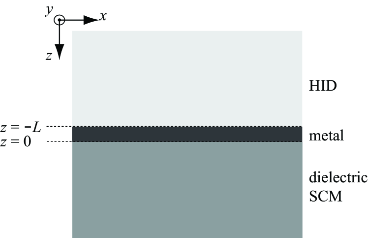
The geometry of the boundary-value problem for the propagation of compound SPP waves is schematically illustrated in Figure 1. The half space is occupied by a HID material with real-valued relative permittivity . An isotropic metal layer of thickness and complex-valued relative permittivity separates the HID material from a dielectric SCM which occupies the half space . The chosen SCM is periodically nonhomogeneous along the axis with period and can be characterized by the relative-permittivity dyadic [2]
| (1) |
where for a right-handed SCM or for a left-handed SCM; the dyadic
| (2) |
contains the principal relative permittivity scalars , , and ; and the rotation dyadics
| (3) | ||||
and
| (4) | ||||
capture the helical nonhomogeneity. Whereas and for cholesteric liquid crystals, and for chiral smectic liquid crystals [16] and chiral sculptured thin films [17]. All three materials are assumed to be nonmagnetic.
Without loss of generality, we consider a compound SPP wave propagating parallel to the unit vector , , in the transverse (i.e., ) plane and decaying far away from the metal layer. The electric and magnetic field phasors can be written everywhere as
| (5) | |||
where is the complex-valued wavenumber. The procedure to obtain a dispersion equation for the wavenumber is provided in detail elsewhere [2]. Once has been numerically determined from that dispersion equation, the piecewise determination of the functions and is also possible.
3 Numerical results
In this section, we present the normalized solutions of the dispersion equation for compound SPP waves. The equation was solved numerically using Mathematica (Version 10) on a Windows XP laptop computer. For all calculations, we fixed nm. The HID material was taken to be SF11 glass () for the results presented in Secs. 3.1 and 3.3, and a lossless dielectric material with a relative permittivity for the results presented in Sec. 3.2. The metal was taken to be silver () with skin depth nm at the chosen wavelength. The dielectric SCM was supposed to be a chiral sculptured thin film made of patinal titanium oxide with nm, , , , and [18]. The angle was set equal to for the results presented in Secs. 3.1 and 3.2. Results for are presented in the Sec. 3.3. The search for solutions was restricted to .
Once a solution of the dispersion equation was found, we determined the field phasors and , and then computed the Cartesian components of the time-averaged Poynting vector
| (6) |
Profiles of the Cartesian components of are presented for representative solutions in this section.
3.1 Effect of the thickness of the silver layer
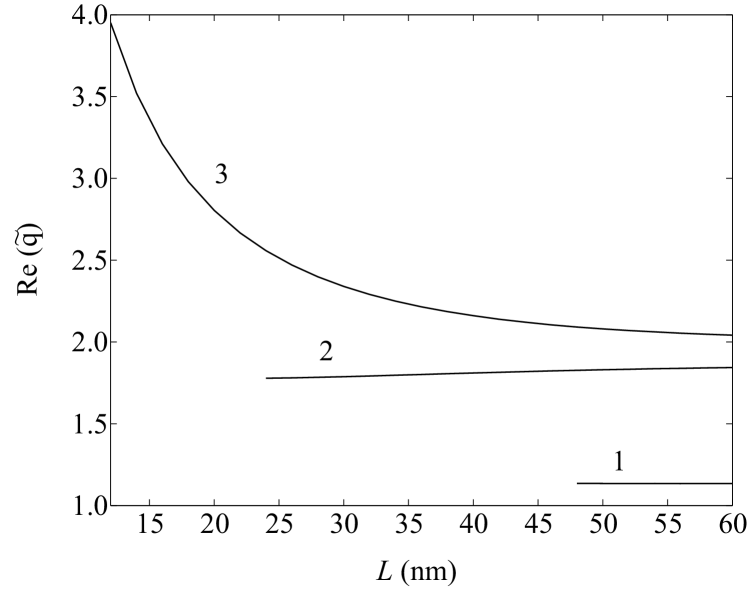
Figures 2 and 3, respectively, show the real part of the normalized wavenumber and the propagation distance in the plane found for all solutions as the thickness of the metal layer was varied from 10 nm to 60 nm, with fixed. As many as three different compound SPP waves can be guided by the chosen HID/metal/SCM structure for nm. These solutions are organized in three branches labeled to in Figs. 2 and 3. Each branch spans the range , the branch being absent for . We determined that nm for branch 1, nm for branch 2, and nm for branch 3.
As increases from , and, therefore, the phase speed , are practically constant on branches 1 and 2; however, the propagation distance decreases. Branch has quite different characteristics: both and increase as increases. However, for a fixed value nm, the solution belonging to branch exhibits the highest value of .
 |
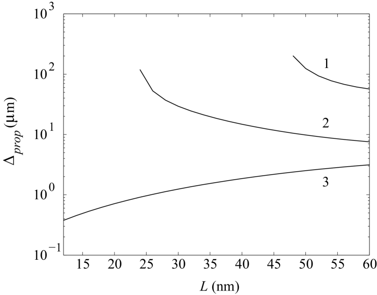 |
Table 1 shows the relative wavenumbers of the compound SPP waves computed for two different thicknesses of the metal layer, nm () and , while is fixed. The table also lists the values of for (a) the SPP waves guided by the metal/SCM interface by itself [15] and (b) the sole -polarized SPP wave guided by the metal/HID interface by itself [4]. When nm, the relative wavenumbers of the compound SPP waves belonging to the branches and are very close to the ones of the SPP wave guided by the metal/SCM interface by itself, while the relative wavenumber of the compound SPP wave belonging to the branch is very close to the one of the SPP wave guided by the metal/HID interface alone. Such affinities indicate that, for this value of , the compound SPP waves on branches and propagate bound predominantly to the metal/SCM interface while the compound SPP wave on branch propagates bound predominantly to the metal/HID interface. Both situations are indicative of a weak coupling between the two metal/dielectric interfaces and . As decreases, solutions on branch 1 remain strongly bound to the metal/SCM interface, but solutions on branches 2 and 3 show stronger coupling between the two metal/dielectric interfaces.
The foregoing conclusions are confirmed by the plots of the spatial profiles of the Cartesian components of the time-averaged Poynting vector . Figure 4 shows the spatial variations of , and for representative compound SPP waves on the three solution branches, when when . From the figure it is evident that the compound SPP wave belonging to branch propagates bound predominantly to the metal/SCM interface with its energy confined mostly to several periods of the SCM close to the metal. The compound SPP wave on branch is bound to the metal/SCM interface only when is large enough, and most of its energy is contained in the first period of the SCM. As decreases, the wave becomes increasingly bound also to the metal/HID interface, thereby indicating a significant coupling between the two metal/dielectric interfaces. The compound SPP wave belonging to branch propagates bound predominantly to the metal/HID interface when nm with a power density confined almost totally in the HID material. The coupling between the two interfaces is clearly evident when nm, the wave then propagating bound to both metal/dielectric interfaces and its energy distributed almost equally in both the HID material and the dielectric SCM.
(a) 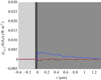 (b)
(b) 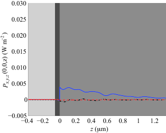
|
(c) 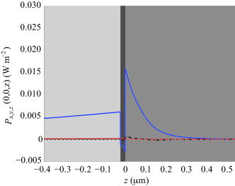 (d)
(d) 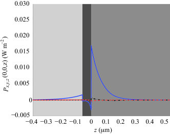
|
(e) 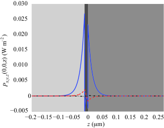 (f)
(f) 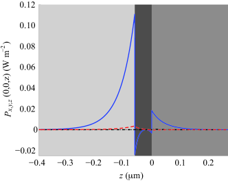
|
| Branch | |||
|---|---|---|---|
| nm | |||
| - | |||
| - | - |
3.2 Effect of the relative permittivity of the HID material
In Sec. 3.1 we showed that the number of the compound SPP waves guided jointly by the two metal/dielectric interfaces reduces (and even vanishes) as the thickness of the metal layer decreases; moreover, no compound SPP wave exists when . In order to investigate the influence of the relative permittivity of the HID material on the number of compound SPP waves, we fixed and nm (i.e., is slightly smaller than ), and varied from to .
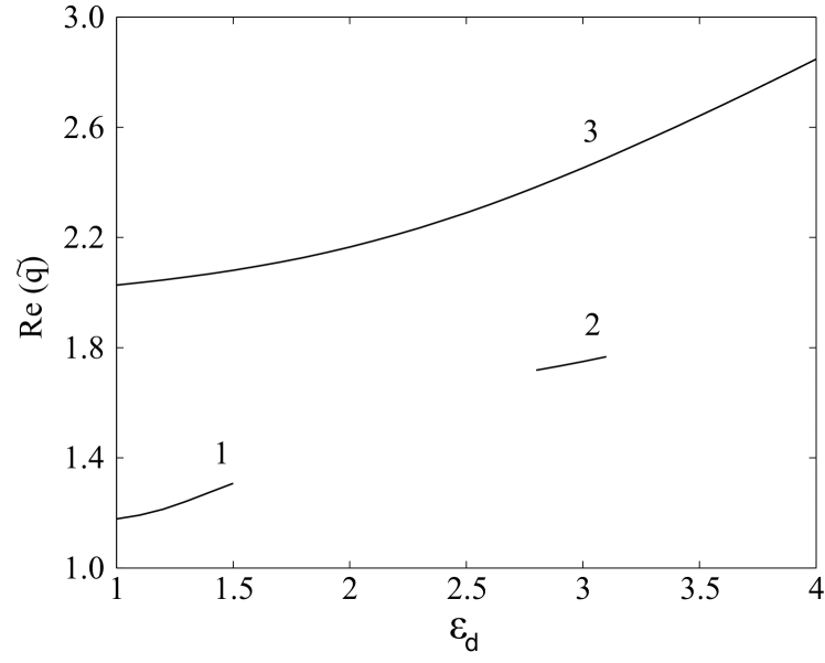
Figures 5 and 6, respectively, show plots of and as functions of . The solutions are organized in three branches labeled to . Two solutions exist in two distinct -intervals: (i) and (ii) . In the remaining parts of the range , only one compound SPP wave exists. As increases, the phase speed increases on all three branches, the increase being almost linear on branches 1 and 2. As increases, the propagation distance first decreases and then increases on branches 1 and 2, but decreases almost linearly on branch 3.
 |
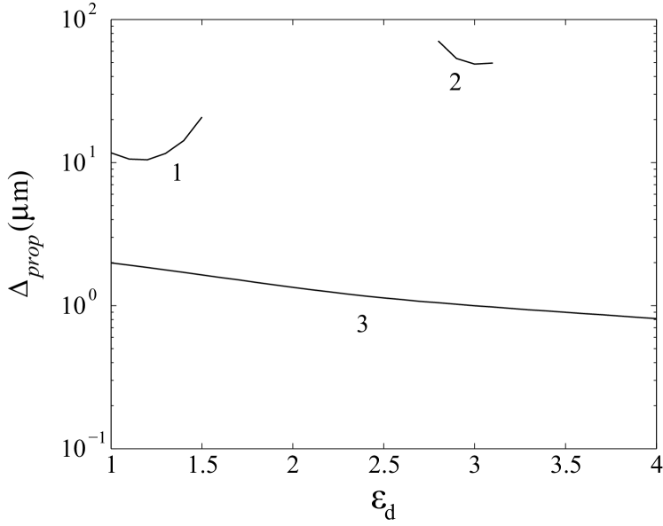 |
Figure 7 shows the spatial profiles of the Cartesian components of the time-averaged Poynting vector for compound SPP waves belonging to the branches and when . Likewise, Fig. 7 shows the spatial profiles of the Cartesian components for compound SPP waves belonging to the branches and when . Due to the significant coupling between the two dielectric/metal interfaces, significant fractions of the energy of the compound SPP waves reside in the both the HID material and the dielectric SCM. When , most of the energy resides in the HID material for the wave on branch and in the dielectric SCM for the wave on branch . When , the energy of the wave is distributed almost equally in both dielectric materials.
(a) 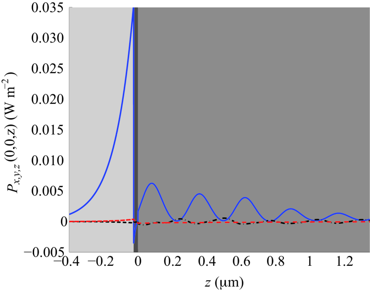
|
(b) 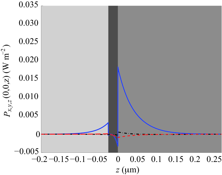
|
(a) 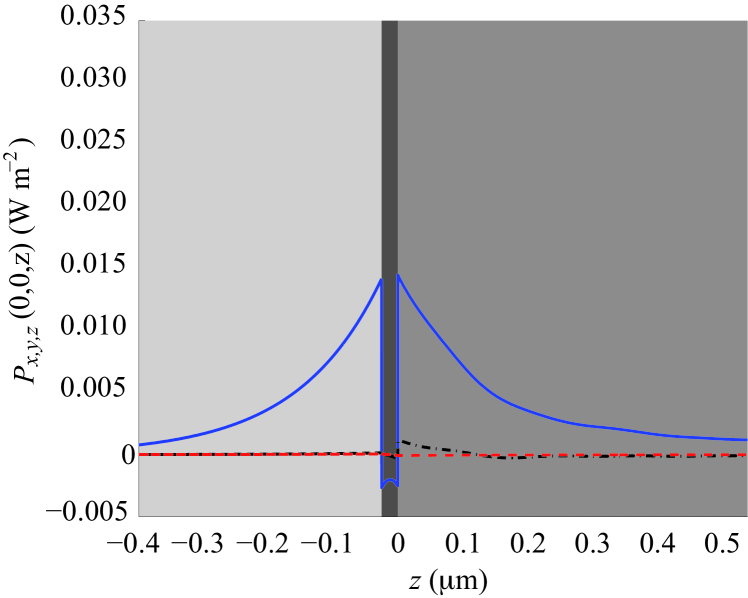
|
(b) 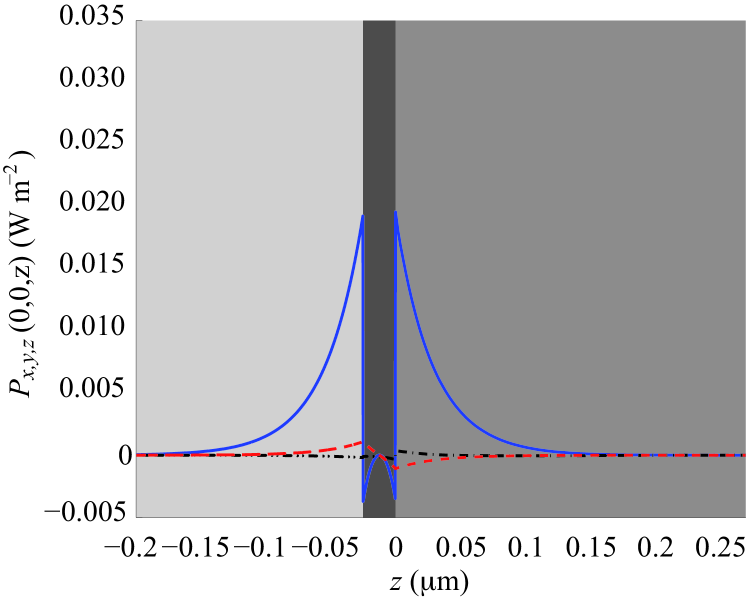
|
3.3 Influence of the transverse anisotropy of the SCM
So far in this paper, we have reported results for . Since an SCM is not isotropic in the plane, the choice of the direction of propagation as quantified through should have an effect. In order to analyze the effect of the anisotropy of the dielectric SCM, we fixed (SF11 glass) and varied for nm. Due to the symmetry of the in the plane, the solutions for are the same for .
Figures 9 and 10, respectively, show plots of and as functions of for nm. In these figures, the solution branches are labeled to be consistent with the data presented in Figs. 2 and 3 for .
For the thinner metal layer ( nm), branch 1 does not exist for any . Whereas branch 2 is confined to , branch 3 spans the entire range . On both branches, Re is almost constant, which implies that is very weakly dependent on . However, whereas is almost independent of on branch 3, it varies by a factor of 10 on branch 2 with a minimum at .
Solution branches 1–3 exist for nm. Two of those branches (labeled 2 and 3) span the entire range of while one (labeled 1) is confined to . Both Re (and, therefore, ) and depend on very weakly on branches 2 and 3. In contrast, Re increases and decreases almost monotonically as increases, but decreases up to where it reaches its minimum and then increases.
Thus, we conclude that some compound SPP waves is not affected greatly by the direction of propagation but others are, depending on metal thickness. A device containing the HID/metal/SCM structure could be rotated about the axis for optimal performance.
(a) 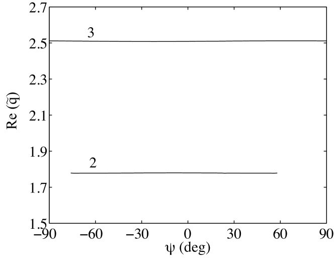
|
(b) 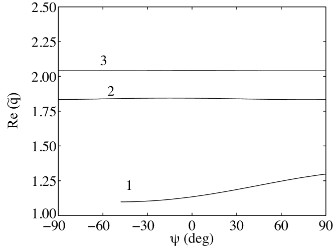
|
(a) 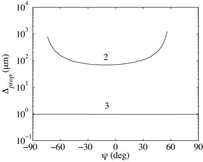
|
(b) 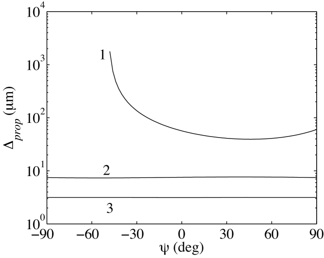
|
4 Concluding remarks
The boundary-value problem for the propagation of compound surface plasmon-polariton waves guided by a thin metal layer sandwiched between a homogeneous isotropic dielectric material and a dielectric structurally chiral material was formulated and solved numerically.
Multiple compound SPP waves, differing in phase speed, attenuation rate and field profile, were found to exist at a fixed frequency (or free-space wavelength, equivalently) only if the thickness of the metal layer is sufficiently large. When the metal thickness is small, the two metal/dielectric interfaces couple to each other, thereby resulting in one or more compound SPP waves that propagate bound to both interfaces with energy lying in both the HID material and the dielectric SCM. As the metal thickness increases, the coupling between the two dielectric/metal interfaces weakens. Eventually, each compound SPP wave is bound predominantly to just one of the two metal/dielectric interfaces with its energy residing mostly in the dielectric partner. If the thickness of the metal layer is greater than the skin depth, the attributes of the compound SPP waves approach those of the SPP waves guided by a metal/dielectric interface alone. The propagation characteristics of some of the compound SPP waves are less affected by the transverse anisotropy of the dielectric SCM than of others.
Thus, the propagation characteristics can be tailored by appropriate choices of the metal thickness, the relative permittivity of the HID material, and the direction of propagation in the transverse plane, once the dielectric SCM has been chosen.
Finally, the multiplicity and the number of compound SPP waves depend on the relative permittivity of the HID material. This feature could be useful for optical sensing applications.
References
- [1] J.M. Pitarke, V.M. Silkin, E.V. Chulkov, P.M. Echenique, Rept. Prog. Phys. 70 (2007) 1–87 (2007).
- [2] J.A. Polo Jr., T.G. Mackay, A. Lakhtakia, Electromagnetic Surface Waves: A Modern Perspective, Elsevier, Waltham, MA, USA, 2013.
- [3] S.E. Swiontek, D.P. Pulsifer, A. Lakhtakia, Sci. Rep. 3 (2013) 1409.
- [4] J. Homola (ed.), Surface Plasmon Resonance Based Sensors, Springer, Berlin, Germany, 2006.
- [5] G. Stabler, M.G. Somekh, C.W. See, J. Microsc. 214 (2004) 328–333.
- [6] J.S. Sekhon, S.S. Verma, Curr. Sci. India 101 (2011) 484–488.
- [7] D. Sarid, Phys. Rev. Lett. 47 (1981) 1927–1930.
- [8] J.C. Quail, J.G. Rako, H.J. Simon, Opt. Lett. 8 (1983) 377–379.
- [9] F. Chiadini, V. Fiumara, A. Scaglione, A. Lakhtakia, J. Nanophoton. 9(1), (2015) 093060.
- [10] E. Reusch, Ann. Phys. Chem. Lpz. 138 (1869) 628–638.
- [11] G. Joly, J. Billard, J. Opt. (Paris) 13 (1982) 227–238.
- [12] S. Chandrasekhar, Liquid Crystals, second ed., Cambridge University Press, Cambridge, United Kingdom, 1992.
- [13] P.G. de Gennes, J.A. Prost, The Physics of Liquid Crystals, second ed., Clarendon Press, Oxford, United Kingdom, 1993.
- [14] K. Robbie, M.J. Brett, A. Lakhtakia, Nature 384 (1996) 616.
- [15] J.A. Polo Jr., A. Lakhtakia, Proc. R. Soc. Lond. A 465 (2009) 87–107.
- [16] I. Abdulhalim, L. Benguigui, R. Weil, J. Phys. (Paris) 46 (1985) 815–825.
- [17] A. Lakhtakia, R. Messier, Sculptured Thin Films: Nanoengineered Morphology and Optics, SPIE Press, Bellingham, WA, USA, 2005.
- [18] I. Hodgkinson, Q.h. Wu, and J. Hazel, Appl. Opt. 37 (1998) 2653–2659.
- [19] J.A. Polo Jr., T.G. Mackay, A. Lakhtakia, J. Opt. Soc. Am. B 28 (2011) 2656–2666.