Electronic structure, spin-orbit coupling, and interlayer interaction in bulk MoS2 and WS2
Abstract
We present in-depth measurements of the electronic band structure of the transition metal dichalcogenides (TMDs) MoS2 and WS2 using angle-resolved photoemission spectroscopy, with focus on the energy splittings in their valence bands at the K point of the Brillouin zone. Experimental results are interpreted in terms of our parallel first-principles computations. We find that interlayer interaction only weakly contributes to the splitting in bulk WS2, resolving previous debates on its relative strength. We additionally find that across a range of TMDs, the band gap generally decreases with increasing magnitude of the valence band splitting, molecular mass, or ratio of the out-of-plane to in-plane lattice constant. Our results provide an important reference for future studies of electronic properties of MoS2 and WS2, and their applications in spintronics and valleytronics devices.
I Introduction
Transition metal dichalcogenides (TMDs) (MX2 where M = Mo or W and X = S, Se, or Te) are layered semiconducting materials that have recently shown promise for application to a wide range of electronic devices, including the growing fields of spintronics and valleytronicsWang et al. (2012). In the monolayer limit, TMDs are theorized to have a split valence band that is nearly fully spin polarizedZhu et al. (2011) near the K and points of the hexagonal Brillouin zone. The spin polarization is predicted to be reversed between the K and points, implying existence of an unusual spin-valley coupling in the TMDs. The ability to selectively populateCao et al. (2012); Xiao et al. (2012); Zeng et al. (2012) these valleys demonstrates their viability for use in spintronics/valleytronics devices.
Despite the importance of the split valence band that governs the unique spin and valley physics of TMDs, there remain questions regarding the origin of these splittings in bulk TMDs. In particular, this splitting is theorized to be entirely a consequence of spin-orbit coupling in the monolayer limit, and a combination of spin-orbit coupling and interlayer interaction in the bulk limit, but there is disagreementKlein et al. (2001); Molina-Sánchez et al. (2013); Alidoust et al. (2014); Eknapakul et al. (2014) about the relative strength of the two mechanisms in the bulk limit. Current electronic band structure studies of bulk MoS2Eknapakul et al. (2014); Jin et al. (2013); Mahatha et al. (2012); Mahatha and Menon (2012, 2013); Suzuki et al. (2014) and WS2Klein et al. (2001) are limited by energy and momentum resolution and lack focus on the valence band splittings. Experimentally, the sizes of the splittings have been characterized, but only with limited resolution.
Here we present high-resolution angle-resolved photoemission spectroscopy (ARPES) data of the electronic band structure of bulk MoS2 and WS2, and analyze our measurements via parallel first-principles computations. Our findings resolve previous debates on the role of interlayer interaction on the valence band splitting, revealing that the splitting in the bulk samples is primarily due to spin-orbit coupling and not interlayer interaction. In order to gain insight into the nature of this splitting, we further investigate its origins, its magnitude, and its correlation with the electronic band gap across a range of TMDs. Our comparisons for various TMDs reveal the interplay between the valence band splitting, band gap, molecular mass, and out-of-plane to in-plane lattice constant ratio, suggesting how specific TMDs would be suited for particular applications.
II Methods
High-resolution ARPES experiments on MoS2 (WS2) were performed at Beamline 10.0.1.1 (4.0.3) of the Advanced Light Source at a temperature of 150 K using 50 eV (52-120 eV) photons. The total energy resolution was 10 meV (20 meV) for experiments on MoS2 (WS2) with an angular resolution () of . The momentum resolution () is related to the angular resolution by where the kinetic energy of the ejected electrons () is dependent on the incident photon energyDamascelli et al. (2003). The samples were cleaved in situ at 150 K in a vacuum better than Torr.
The electronic structures of MX2 (M = Mo or W and X = S, Se, or Te) were computed using the projector augmented wave methodBlöchl (1994); Kresse and Joubert (1999) as implemented in the VASPKresse and Hafner (1993); Kresse and Furthmüller (1996a, b) package within the generalized gradient approximation (GGA)Perdew et al. (1996) scheme. A Monkhorst-Pack k-point mesh was used in the computations. We used experimental lattice constants and relaxed the atomic positions until the residual forces were less than 0.001 eV/Å. The spin-orbit coupling effects were included self-consistently. In order to correct the energy band gaps, we also performed calculations with the HSE hybrid functionalHeyd et al. (2003, 2006).
Single crystals were synthesized using the Br2 vapor transport technique in a two-zone furnace system. Mo, W, and S powders (purity 99.9995%) were mixed in stoichiometric ratios in a sealed quartz tube at Torr pressure and annealed to for one week to yield precursor powders. Next, they were loaded into 2 inch diameter tubes with Br2 liquid, pumped down to Torr, and sealed. Typical growth parameters were established as heat up for one week from room temperature to , the low temperature zone was set to in one day, and the system was kept at this temperature for three weeks and controllably cooled down to room temperature in one week. Synthesized crystals displayed strong Raman signals at 384 cm-1 and 407 cm-1 for MoS2, and 352 cm-1 and 417 cm-1 for WS2. Lastly, monolayers exfoliated from MoS2 and WS2 crystals displayed sharp bright luminescence peaks at 1.88 eV and 2.04 eV, respectively.
III Results And Discussion
III.1 Characterizing the Origins of the Splitting
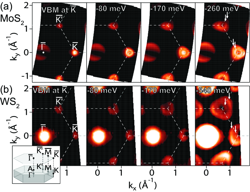
Fig. 1(a) and 1(b) show detailed momentum-resolved constant-energy maps for bulk MoS2 and WS2, respectively. The two-dimensional (reduced in the dimension as shown in the inset) hexagonal Brillouin zone is overlaid as white dashed lines. The observed suppression of intensity in MoS2 along a specific momentum direction near is due presumably to matrix element effectsBansil and Lindroos (1999); *Sahrakorpi2005; *Bansil2005. The evolution of the valence band about the , , and points can be clearly observed throughout the range of binding energies shown. We offset the two sets of data so that the valence band maximum at is shown at the same energy and we compare the two band structures as binding energy is increased. The two samples produce similar spectra with the most notable difference being the appearance of the lower split valence band at at approximately 170 meV below the local valence band maximum (VBM) for MoS2. This appears as a small circular feature centered at within a larger concentric feature. The analogous splitting for WS2 becomes apparent in the spectra at much higher binding energy, as seen in the map at 540 meV below the VBM. The splitting for both samples is shown by vertical white arrows. Trigonal warping of the valence band in the vicinity of the and points, similar to that seen in other bulk TMDsAlidoust et al. (2014); Suzuki et al. (2014), is observed for both samples and presented here for the first time for bulk WS2. This deviation from a circular feature about and is more pronounced at higher binding energies where the feature becomes more triangular. An analogous trigonal warping has been predictedRostami et al. (2013); Kormányos et al. (2013) to occur in monolayer MoS2 samples as a consequence of the orbital structure of these bands and anisotropic (order ) corrections to the energy but has not been observed so far in an ARPES experiment.
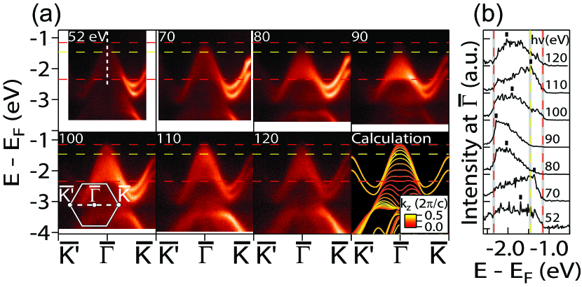
To obtain information about the dispersion, i.e. the interlayer dispersion, in Figure 2(a) we show detailed photon energy dependent maps compared with -resolved theoretical calculations of bulk WS2 along the – high symmetry direction. Indeed, at normal emission (), is related to the kinetic energy of the ejected electrons () by where is the inner potential determined from the measured dispersionHimpsel (1983); Hüfner (2003). Near , we observe a broad feature likely associated with the convolution of the various bands predicted for different values as it extends between the two horizontal red dashed lines corresponding to the calculated energies of the top two valence bands at (). The top of this broad feature aligns well with the calculated valence band maximum at () for the 52 eV map and as the photon energy is increased further, the top of the feature decreases in energy until it aligns with the calculated valence band maximum at the A point (, ) indicated by the horizontal yellow dashed line in the 90 eV map. Increasing the photon energy further returns the top of the valence band feature to its maximum value.
The observed dispersion at is investigated more closely in Fig. 2(b) by comparing energy distribution curves (EDCs) taken at for each of the incident photon energies (e.g. along the dashed white line in the 52 eV image in (a)). The observation of a large spread in energy of the main peak in the EDC spectra between the calculated energies of the top two valence bands at (vertical red dashed lines) is in agreement with the association of the broad feature near with the convolution of multiple bands predicted for different values. The peak intensity (tick mark) moves up and down in binding energy in a periodic manner confirming the strong dependence of these bands. Overall, our observed dispersions agree well with other predictions for WS2Klein et al. (2001) and our calculations which predict wide variation in binding energy (up to 880 meV) of the bands as changes from 0 to . Similar dispersions are also found theoretically and experimentally more generally in TMDsBöker et al. (2001); Fives et al. (1992); Mattheiss (1973); Coehoorn et al. (1987).
Near , we observe the band splitting at the top of the valence bands for all photon energies, indicating that the splitting occurs for all corresponding values. We measure the magnitude of the splitting to vary between 414 meV and 441 meV in accordance with our corresponding predicted range of 410 meV () to 466 meV (). This relatively small change in magnitude of the splitting (27 meV experimentally and 56 meV theoretically) across this range of photon energies indicates weak dispersion near and . This is in contrast to the observation of large variations in the spectra of the broad feature at which indicates strong dispersion of the bands near .
As a result of the layered structure of bulk TMDs, the three-dimensional character of the band structure is directly related to the strength of the interlayer interaction. The strong dispersion at is a reflection of the three-dimensional character of those bands. However, the relatively weak dispersion at and is a reflection of the two-dimensional character of those bands and shows that interlayer interaction has a weak effect on the valence band splitting. Hence, we conclude that the splitting is dominated by spin-orbit coupling with interlayer interaction playing a minor role.
III.2 The Effect of Spin-Orbit Coupling on the Valence Band Structure
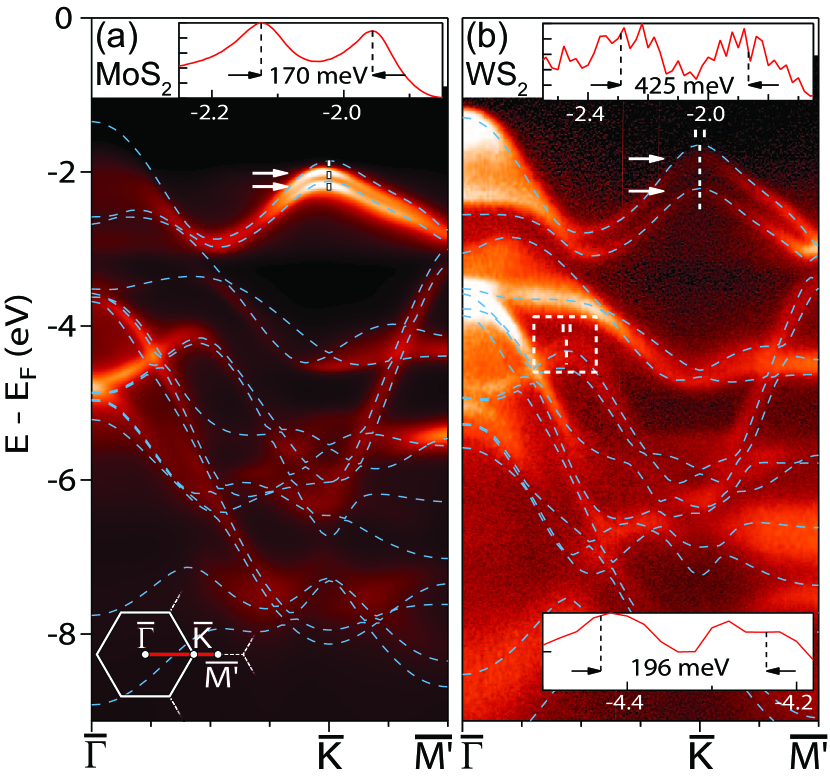
Figure 3 shows high-resolution energy versus momentum maps of the band structure of bulk MoS2 (panel a) and WS2 (panel b). Band dispersions can be seen as far as 8 eV below the Fermi energy; many of these bands have not been observed before. The experimental band structure shows remarkable agreement with our theoretical predictions (blue dashed lines) throughout this energy and momentum region. The intensity of the valence band maximum near for MoS2 is reduced due presumably to matrix element effectsBansil and Lindroos (1999); *Sahrakorpi2005; *Bansil2005. Additionally, intensity of the experimental bands with low binding energy may be shifted near due to their strong dependence (as shown for WS2 in Fig. 2). The splitting of the valence band at is fully resolved for both samples (as indicated by the white arrows) and is found to be 170 2 meV for MoS2 and 425 18 meV for WS2 (as shown in the upper insets). The value for MoS2 agrees well with our experimental constant energy maps presented in Fig. 1(a) as the lower split band for MoS2 appears 170 meV below the higher split band. The value for WS2 is consistent with our experimental constant energy maps in Fig. 1(b) as the lower split band is not visible 170 meV below the higher split band, but is clearly visible 540 meV below. These measured magnitudes are smaller by approximately 100 meV than the values of 265 meV for MoS2 and 570 meV for WS2 predicted by HSE-based calculations. However, our experimental values agree very well with GGA-based calculations that predict a splitting of 145-224 meV for MoS2 and 410-466 meV for WS2 across all values. The large difference in magnitude between the splittings for MoS2 and WS2 can be explained by the larger intrinsic spin-orbit coupling of tungsten compared with that of molybdenum. Additionally, our calculations predict a substantial splitting of a valence band of WS2 at high binding energy (see white dashed rectangle). The maximum splitting predicted is in agreement with the experimental value of 196 22 meV extracted from the EDC spectra (bottom inset) where two clear peaks can be distinguished. Similar to the splitting in the top valence band, we predict this band to be split largely due to spin-orbit coupling and only partially by interlayer interaction.
III.3 Relationship between Band Gap and Spin-Orbit Splitting
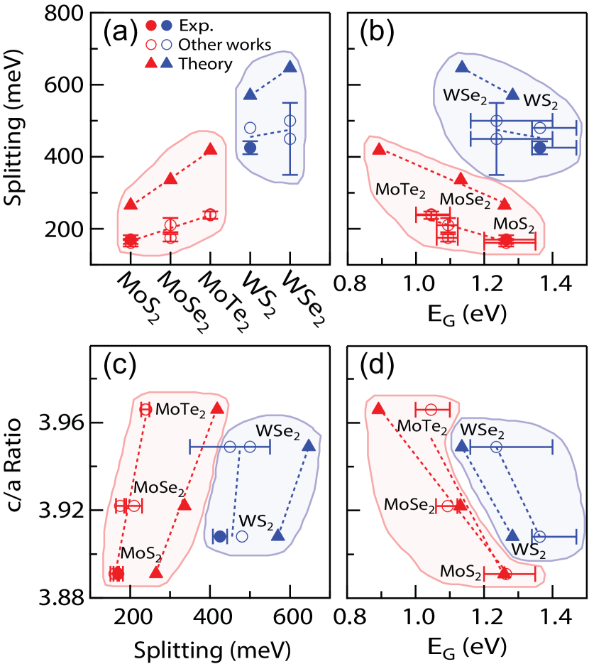
Figure 4(a) shows the magnitude of valence band splitting for bulk MoS2, WS2, and other bulk TMDs. The molybdenum- and tungsten-based TMDs are ordered separately from left to right with increasing molecular mass. For a given transition metal, the magnitude of the splitting increases as molecular mass increases. These trends are shown by the dashed lines and can be explained as a consequence of the larger intrinsic spin-orbit coupling of the successively heavier atoms. The same general trend is obtained from HSE hybrid functional calculations (triangles), although the splitting appears to be approximately 100 meV larger. Figure 4(c) shows the ratio of out-of-plane to in-plane lattice constant () versus the magnitude of valence band splitting. Similar to the molecular mass trend, we observe that for a given transition metal, the magnitude of splitting increases with increasing ratio; however, our calculations indicate that although this trend holds across a range of TMDs, it does not hold for individual TMDs.
In addition to the valence band splitting, the band gap plays a key role when considering TMDs for use in spintronics/valleytronics devices. Figure 4(b) shows the magnitude of valence band splitting versus band gap (EG) for bulk MoS2, WS2, and other bulk TMDs. For a given transition metal, the band gap of bulk TMDs decreases with increasing valence band splitting. The same trend is observed as a function of molecular mass in that the band gap decreases with increasing molecular mass. Again, this trend is seen for both experimental and theoretical data even though the magnitude of the splitting for each TMD is calculated to be approximately 100 meV larger than the corresponding experimental values. Figure 4(d) shows the ratio of out-of-plane to in-plane lattice constant versus band gap. It too follows the same trend as molecular mass and valence band splitting in that the band gap decreases with increasing ratio. This strong relationship between the band gap, the valence band splitting, and ratio would help guide the search for suitable TMDs targeted at specific applications.
III.4 Conclusions
We have presented in-depth high-resolution ARPES studies of the electronic band structure of bulk MoS2 and WS2 together with detailed first-principles computations. We have shown that the valence band splitting in bulk WS2 is primarily due to spin-orbit coupling and not interlayer interaction, resolving previous debates on their relative role. These results strengthen the connection between bulk and monolayer TMDs as the splitting in the monolayer limit is due entirely to spin-orbit coupling. We have shown how the magnitude of this splitting changes for various TMDs and how it correlates with molecular mass, ratio, and band gap. These results provide important new information on how to control these parameters in TMDs and for the development of TMD-based devices in the fields of spintronics and valleytronics.
Acknowledgements.
We thank C. Hwang, C. L. Smallwood, and G. Affeldt for useful discussions. The ARPES work was supported by the sp2 Program at Lawrence Berkeley National Laboratory, funded by the U.S. Department of Energy, Office of Science, Office of Basic Energy Sciences, Materials Sciences and Engineering Division, under Contract No. DE-AC02-05CH11231. The Advanced Light Source is supported by the Director, Office of Science, Office of Basic Energy Sciences, of the U.S. Department of Energy under Contract No. DE-AC02-05CH11231. The electronic structure calculations at Northeastern University were supported by the US Department of Energy (DOE), Office of Science, Basic Energy Sciences grant number DE-FG02-07ER46352 (core research), and benefited from Northeastern University’s Advanced Scientific Computation Center (ASCC), the NERSC supercomputing center through DOE grant number DE-AC02-05CH11231, and support (applications to layered materials) from the DOE EFRC: Center for the Computational Design of Functional Layered Materials (CCDM) under DE-SC0012575. TRC and HTJ are supported by the National Science Council and Academia Sinica, Taiwan. H.L. acknowledges the Singapore National Research Foundation for support under NRF Award No. NRF-NRFF2013-03. We also thank NCHC, CINC-NTU, and NCTS, Taiwan for technical support.References
- Wang et al. (2012) Q. H. Wang, K. Kalantar-Zadeh, A. Kis, J. N. Coleman, and M. S. Strano, Nat Nano 7, 699 (2012).
- Zhu et al. (2011) Z. Y. Zhu, Y. C. Cheng, and U. Schwingenschlögl, Phys. Rev. B 84, 153402 (2011).
- Cao et al. (2012) T. Cao, G. Wang, W. Han, H. Ye, C. Zhu, J. Shi, Q. Niu, P. Tan, E. Wang, B. Liu, and J. Feng, Nat Commun 3, 887 (2012).
- Xiao et al. (2012) D. Xiao, G.-B. Liu, W. Feng, X. Xu, and W. Yao, Phys. Rev. Lett. 108, 196802 (2012).
- Zeng et al. (2012) H. Zeng, J. Dai, W. Yao, D. Xiao, and X. Cui, Nat Nano 7, 490 (2012).
- Klein et al. (2001) A. Klein, S. Tiefenbacher, V. Eyert, C. Pettenkofer, and W. Jaegermann, Phys. Rev. B 64, 205416 (2001).
- Molina-Sánchez et al. (2013) A. Molina-Sánchez, D. Sangalli, K. Hummer, A. Marini, and L. Wirtz, Phys. Rev. B 88, 045412 (2013).
- Alidoust et al. (2014) N. Alidoust, G. Bian, S.-Y. Xu, R. Sankar, M. Neupane, C. Liu, I. Belopolski, D.-X. Qu, J. D. Denlinger, F.-C. Chou, and M. Z. Hasan, Nat Commun 5, (2014).
- Eknapakul et al. (2014) T. Eknapakul, P. D. C. King, M. Asakawa, P. Buaphet, R.-H. He, S.-K. Mo, H. Takagi, K. M. Shen, F. Baumberger, T. Sasagawa, S. Jungthawan, and W. Meevasana, Nano Letters, Nano Lett. 14, 1312 (2014).
- Jin et al. (2013) W. Jin, P.-C. Yeh, N. Zaki, D. Zhang, J. T. Sadowski, A. Al-Mahboob, A. M. van der Zande, D. A. Chenet, J. I. Dadap, I. P. Herman, P. Sutter, J. Hone, and R. M. Osgood, Phys. Rev. Lett. 111, 106801 (2013).
- Mahatha et al. (2012) S. K. Mahatha, K. D. Patel, and K. S. R. Menon, Journal of Physics: Condensed Matter 24, 475504 (2012).
- Mahatha and Menon (2012) S. K. Mahatha and K. S. R. Menon, Journal of Physics: Condensed Matter 24, 305502 (2012).
- Mahatha and Menon (2013) S. K. Mahatha and K. S. R. Menon, Journal of Physics: Condensed Matter 25, 115501 (2013).
- Suzuki et al. (2014) R. Suzuki, M. Sakano, Y. J. Zhang, R. Akashi, D. Morikawa, A. Harasawa, K. Yaji, K. Kuroda, K. Miyamoto, T. Okuda, K. Ishizaka, R. Arita, and Y. Iwasa, Nat Nano 9, 611 (2014).
- Damascelli et al. (2003) A. Damascelli, Z. Hussain, and Z.-X. Shen, Rev. Mod. Phys. 75, 473 (2003).
- Blöchl (1994) P. E. Blöchl, Phys. Rev. B 50, 17953 (1994).
- Kresse and Joubert (1999) G. Kresse and D. Joubert, Phys. Rev. B 59, 1758 (1999).
- Kresse and Hafner (1993) G. Kresse and J. Hafner, Phys. Rev. B 48, 13115 (1993).
- Kresse and Furthmüller (1996a) G. Kresse and J. Furthmüller, Computational Materials Science 6, 15 (1996a).
- Kresse and Furthmüller (1996b) G. Kresse and J. Furthmüller, Phys. Rev. B 54, 11169 (1996b).
- Perdew et al. (1996) J. P. Perdew, K. Burke, and M. Ernzerhof, Phys. Rev. Lett. 77, 3865 (1996).
- Heyd et al. (2003) J. Heyd, G. E. Scuseria, and M. Ernzerhof, The Journal of Chemical Physics 118, 8207 (2003).
- Heyd et al. (2006) J. Heyd, G. E. Scuseria, and M. Ernzerhof, The Journal of Chemical Physics 124, 219906 (2006).
- Bansil and Lindroos (1999) A. Bansil and M. Lindroos, Phys. Rev. Lett. 83, 5154 (1999).
- Sahrakorpi et al. (2005) S. Sahrakorpi, M. Lindroos, R. S. Markiewicz, and A. Bansil, Phys. Rev. Lett. 95, 157601 (2005).
- Bansil et al. (2005) A. Bansil, M. Lindroos, S. Sahrakorpi, and R. S. Markiewicz, Phys. Rev. B 71, 012503 (2005).
- Rostami et al. (2013) H. Rostami, A. G. Moghaddam, and R. Asgari, Phys. Rev. B 88, 085440 (2013).
- Kormányos et al. (2013) A. Kormányos, V. Zólyomi, N. D. Drummond, P. Rakyta, G. Burkard, and V. I. Fal’ko, Phys. Rev. B 88, 045416 (2013).
- Himpsel (1983) F. J. Himpsel, Advances in Physics, Advances in Physics 32, 1 (1983).
- Hüfner (2003) S. Hüfner, Photoelectron Spectroscopy: Principles and Applications, 3rd ed. (Springer Berlin Heidelberg, 2003).
- Böker et al. (2001) T. Böker, R. Severin, A. Müller, C. Janowitz, R. Manzke, D. Voß, P. Krüger, A. Mazur, and J. Pollmann, Phys. Rev. B 64, 235305 (2001).
- Fives et al. (1992) K. Fives, I. T. McGovern, R. McGrath, R. Cimino, G. Hughes, A. McKinley, and G. Thornton, Journal of Physics: Condensed Matter 4, 5639 (1992).
- Mattheiss (1973) L. F. Mattheiss, Phys. Rev. B 8, 3719 (1973).
- Coehoorn et al. (1987) R. Coehoorn, C. Haas, J. Dijkstra, C. J. F. Flipse, R. A. de Groot, and A. Wold, Phys. Rev. B 35, 6195 (1987).
- Böker et al. (1999) T. Böker, A. Müller, J. Augustin, C. Janowitz, and R. Manzke, Phys. Rev. B 60, 4675 (1999).
- Yu et al. (1999) S.-W. Yu, T. Lischke, R. David, N. Müller, U. Heinzmann, C. Pettenkofer, A. Klein, A. Perlov, E. Krasovskii, W. Schattke, and J. Braun, Journal of Electron Spectroscopy and Related Phenomena 101–103, 449 (1999).
- Finteis et al. (1997) T. Finteis, M. Hengsberger, T. Straub, K. Fauth, R. Claessen, P. Auer, P. Steiner, S. Hüfner, P. Blaha, M. Vögt, M. Lux-Steiner, and E. Bucher, Phys. Rev. B 55, 10400 (1997).
- Kam and Parkinson (1982) K. K. Kam and B. A. Parkinson, The Journal of Physical Chemistry, J. Phys. Chem. 86, 463 (1982).
- Aruchamy (1992) A. Aruchamy, Photoelectrochemistry and Photovoltaics of Layered Semiconductors, Physics and Chemistry of Materials with Low-Dimensional Structures (Springer Netherlands, 1992).
- Gmelin (1992) L. Gmelin, Gmelin Handbook of Inorganic and Organometallic Chemistry. Mo - Molybdenum. Supplement Vol. B 7, 8, 9. (Springer, 1992).
- Kam et al. (1984) K. K. Kam, C. L. Chang, and D. W. Lynch, Journal of Physics C: Solid State Physics 17, 4031 (1984).
- Braga et al. (2012) D. Braga, I. Gutiérrez Lezama, H. Berger, and A. F. Morpurgo, Nano Letters, Nano Lett. 12, 5218 (2012).
- Traving et al. (1997) M. Traving, M. Boehme, L. Kipp, M. Skibowski, F. Starrost, E. E. Krasovskii, A. Perlov, and W. Schattke, Phys. Rev. B 55, 10392 (1997).
- Schutte et al. (1987) W. Schutte, J. De Boer, and F. Jellinek, Journal of Solid State Chemistry 70, 207 (1987).