Dielectric Engineered Tunnel Field-Effect Transistor
Abstract
The dielectric engineered tunnel field-effect transistor (DE-TFET) as a high performance steep transistor is proposed. In this device, a combination of high-k and low-k dielectrics results in a high electric field at the tunnel junction. As a result a record ON-current of about 1000 uA/um and a subthreshold swing (SS) below 20mV/dec are predicted for WTe2 DE-TFET. The proposed TFET works based on a homojunction channel and electrically doped contacts both of which are immune to interface states, dopant fluctuations, and dopant states in the band gap which typically deteriorate the OFF-state performance and SS in conventional TFETs.
Index Terms:
TFETs, dielectric engineering, electrical doping.I Introduction
Tunnel FETs (TFETs) are strong candidates for future electronics applications due to their promise of low power consumption originating from their subthreshold-swing (SS) being less than the conventional limit of 60 mV/dec [1]. However, TFETs usually suffer from lower ON-currents if compared to ultra-scaled MOSFETs [2], since their currents are the result of the tunneling process. To overcome the low ON-current challenge, two obvious solutions are: 1) Increasing the electric field at the tunnel junction, 2) decreasing the band gap and effective mass of the channel material. However, reducing the band gap increases the OFF-current of the device and limits the maximum allowable supply voltage VDD. Accordingly, there is a lower limit on the band gap for any VDD ().
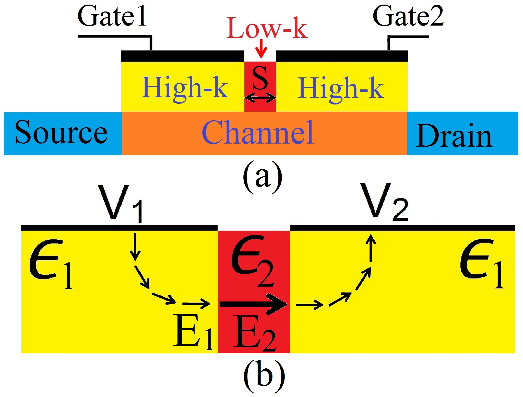
Previous approaches for increasing the electric field at the tunnel junction included using an internal field (i.e. piezo-electric field) in nitride heterostructures [3] or employing 2D channel materials with tight gate control [4, 5]. In this work, a new method for increasing the electric field is proposed. It is shown that using a low-k dielectric next to high-k dielectrics can, in principle, increase the electric field in homo-junction TFETs significantly. The structure of the dielectric engineered TFET (DE-TFET) is shown in Fig. 1a. At the interface between the dielectrics, the displacement vector should be continuous (). With , the low-k dielectric has a larger electric field as illustrated in Fig. 1b. Since the high electric field region occurs right at the top of the tunnel junction, the ON-current of the device is amplified. Notice that the same idea (combination of high-k and low-k dielectrics) can be used in other device structures; e.g. gate-all-around, double and single gated TFETs.
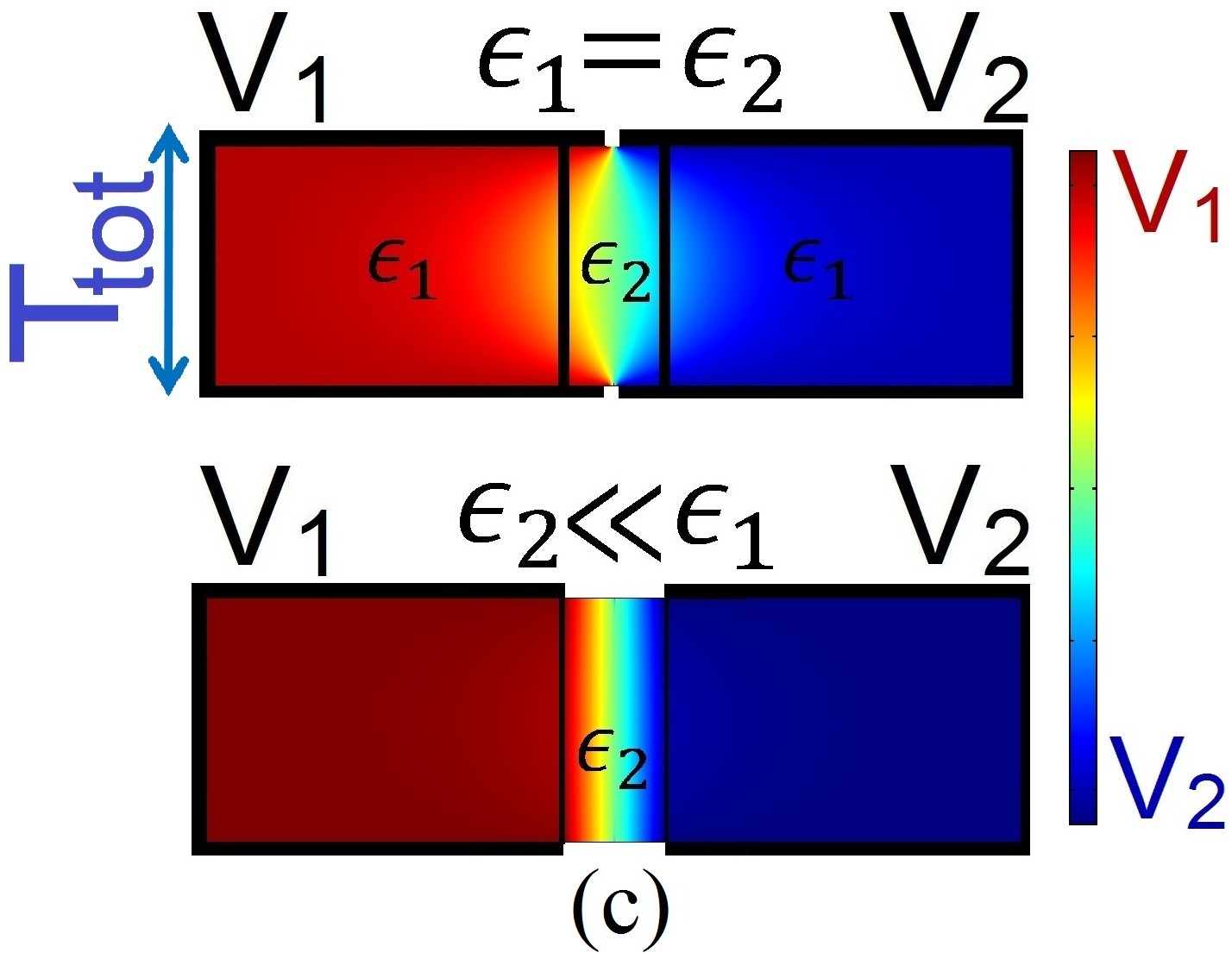
Fig. 1c compares the potential profile for a conventional electrically doped TFET (ED-TFET) [6] with that of a DE-TFET. In case of the ED-TFETs, the width of the potential spread is proportional to the total thickness of the device (the body thickness plus the oxide thickness shown as in Figs. 1c and 2a). In contrast, most of the potential drop in the DE-TFET occurs over the width of the low-k dielectric region (labeled as in Fig. 1a). Equation (1) compares the average electric field of a conventional ED-TFET with that of the DE-TFET showing a possible gain in the electric field for the DE-TFET (as long as ).
| (1) |
Furthermore, the DE-TFET offers several other advantages: 1) The performance is not very sensitive to the spacing (shown as in Fig. 1) when is chosen around the optimum value, in contrast to the conventional ED-TFET in which the ON-current decreases monotonically with increasing [6] (i.e. lack of optimum : ). 2) Increasing the oxide thickness does not deteriorate the performance of the device, while the performance of electrically doped devices strongly depends on the thickness [6]. 3) There is no need for chemical doping which means the DE-TFET does not exhibit the drawbacks of chemically doped devices [7] (i.e. dopant states in the bandgap which deteriorate the OFF-state performance and SS in addition to the disorder introduced by fluctuations in dopant locations). Note that despite the oxide thickness having less impact on the performance of the DE-TFETs compared to ED-TFETs, a thinner oxide is still slightly beneficial for an improved ON-state.
In Section III, full-band quantum transport simulations are performed on a monolayer WTe2 homojunction DE-TFET to investigate its performance. The performance sensitivity of the DE-TFETs to the spacing, thickness, and channel material (WSe2 and WTe2) is discussed by both analytic modeling and numerical simulations in Section IV.
II Simulation details
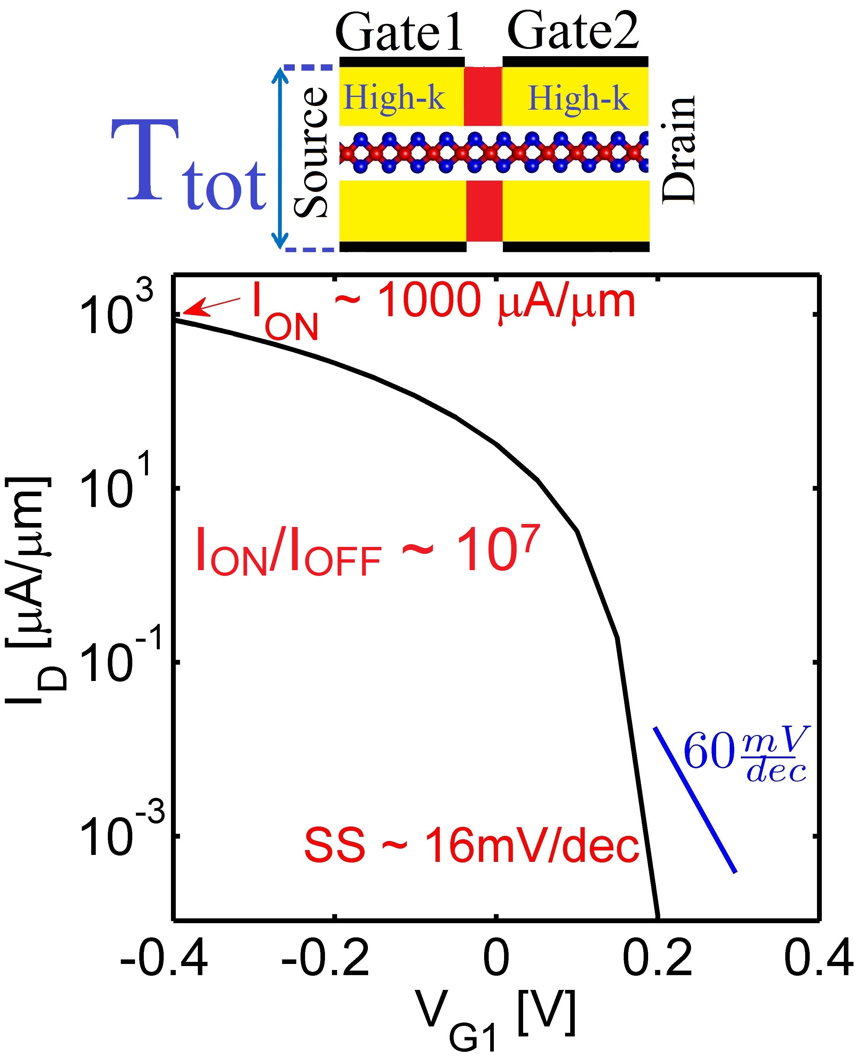
To represent WSe2 and WTe2 as channel materials of the DE-TFET atomistically, we have utilized a sp3d5 2nd nearest neighbor tight-binding model with spin-orbit coupling. Atomistic quantum transport simulations employing a self-consistent Poisson-NEGF (Non-equilibirum Green’s Function) method have been utilized. The details of the simulation methods and material properties can be found in [4]. The simulated double gated DE-TFETs assume a structure shown in Fig. 1a. Each gate has a length of 12nm, with the low-k spacing . Notice that the low-k dielectric fills the space between the gates, right on top of the tunnel junction. A source-drain voltage of 0.8V is used throughout, and the relative dielectric constants of high-k and low-k dielectrics are set to 20 and 1 (i.e. air gap) respectively unless mentioned otherwise. The total thickness of the device equals 4.4nm by default, including the body thickness of the channel (0.7nm). All of the transport simulations have been performed with the simulation tool NEMO5 [8].
III Simulation results
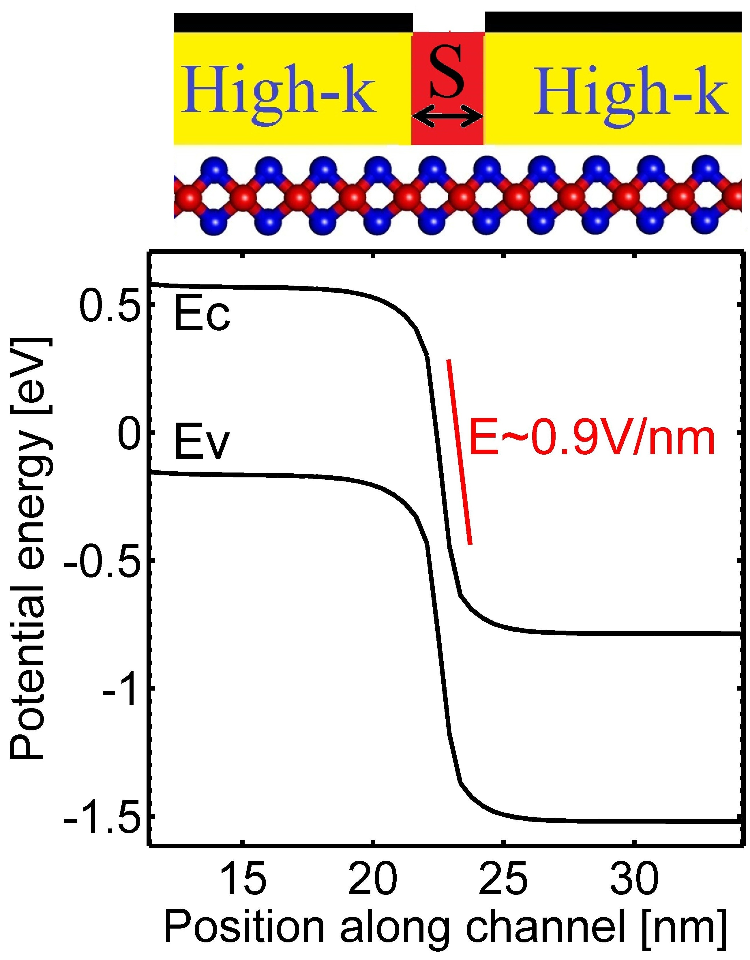
Fig. 2a shows transfer characteristics of a monolayer WTe2 DE-TFET with an ON-current of about 1000 uA/um and SS of 16 mV/dec. This is a record ION-value among all reported ON-currents from full band atomistic simulations of planar homojunction steep devices [9]. Having a high ON-current without using a hetero-junction and chemical doping has advantages in terms of OFF-state performance. Chemical doping can introduce dopant states within the band gap [7], and hetero-junctions often suffer from interface states. Both of these effects increase SS of the device. Fig. 2b shows the conduction and valence band profiles of the WTe2 DE-TFET. The electric field at the tunnel junction is about 0.9 V/nm. This large value of electric field and ON-current is due to the presence of the low-k dielectric ().
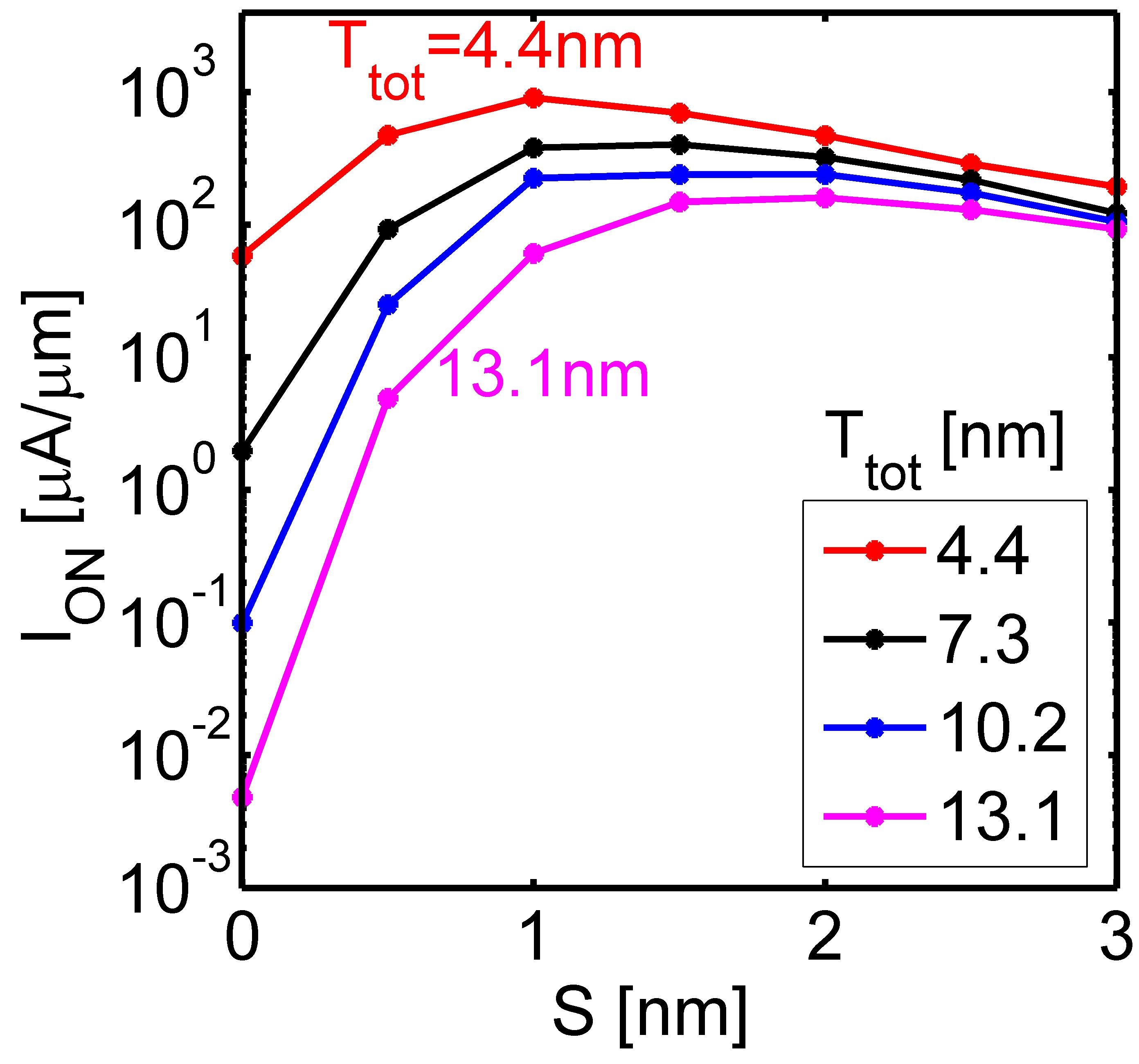
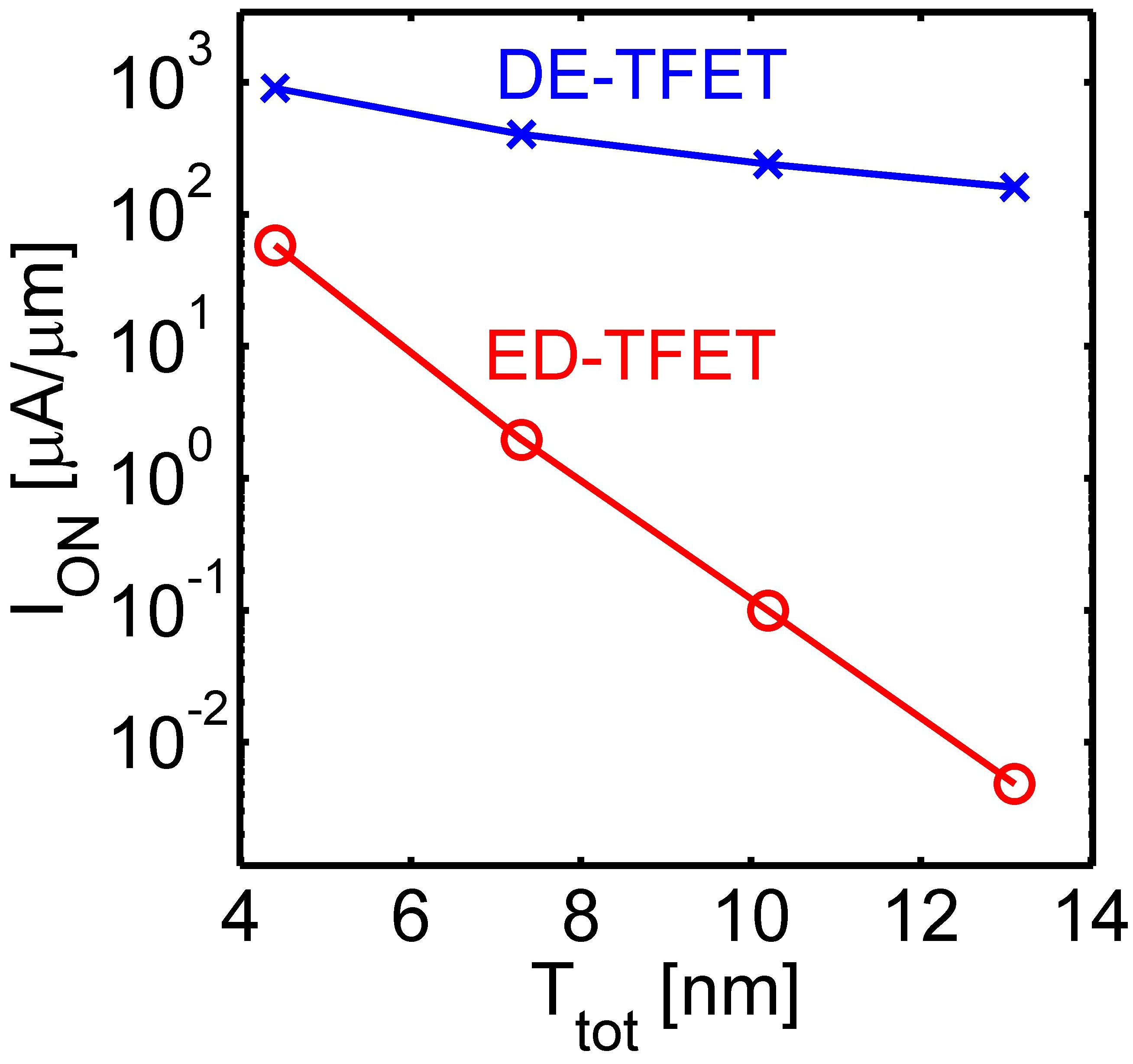
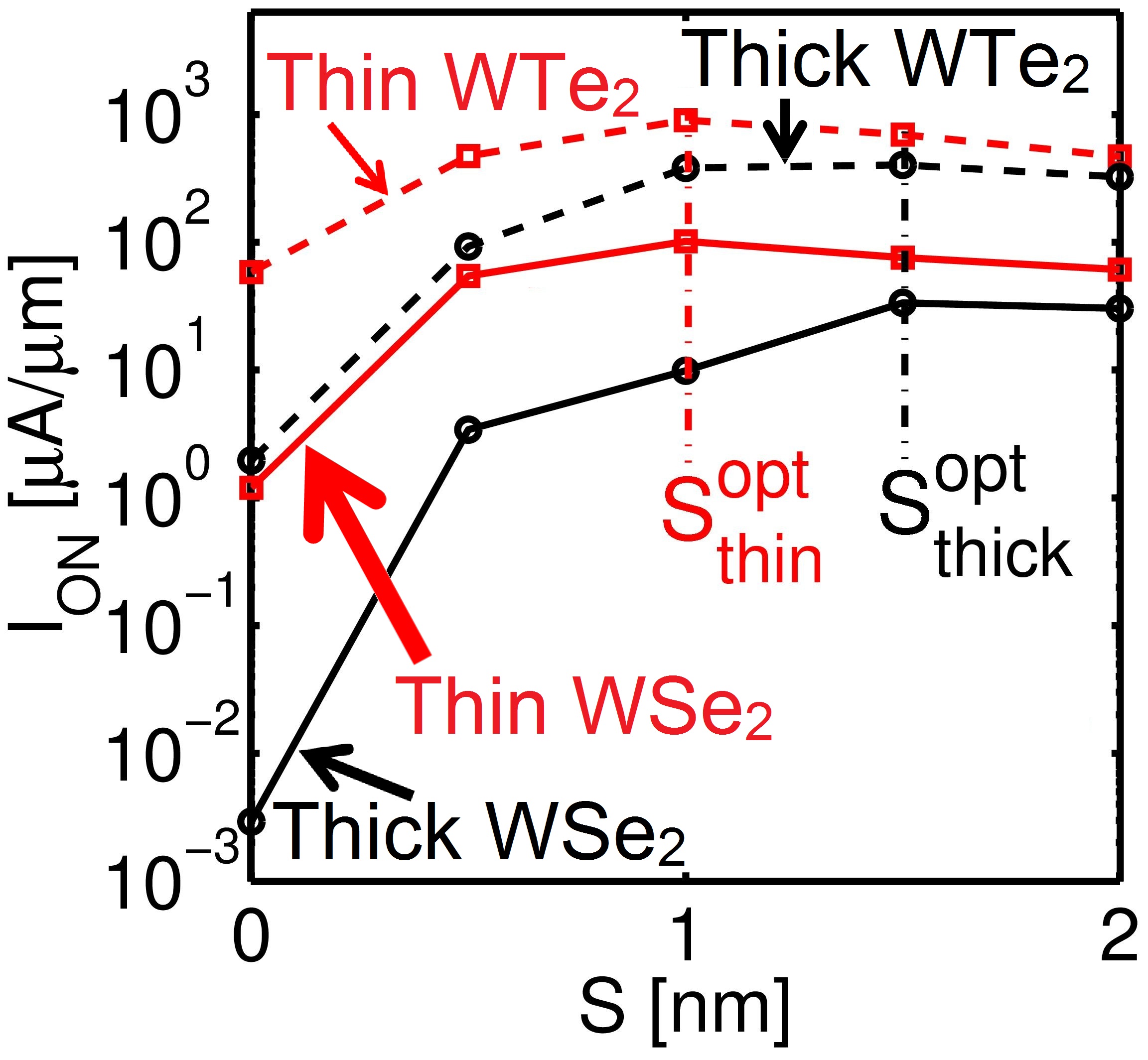
The ON-current of a WTe2 DE-TFET as a function of low-k spacing is shown in Fig. 2c. The optimum spacing to gain the maximum ON-current depends on the total thickness of the device (shown as in Fig. 2a). For example, the optimum varies from about 1nm to 2nm when changes from 4.4nm to 10.2nm. Fig. 2d compares the performance sensitivity of the WTe2 DE-TFET with the conventional ED-TFET. The performance of the DE-TFET is much less sensitive to oxide thickness variations if compared to the conventional ED-TFET.
IV Analytical Modeling
It is apparent that the width of the low-k dielectric () affects the performance of DE-TFETs. When equals 0, the device converts to a conventional ED-TFET and the electric field at the tunnel junction reduces. On the other hand, when becomes very large, the electric field reduces to 0. Accordingly, there exists an optimum spacing where the electric field is high. Notice that achieving the highest electric field is not a sufficient condition to ensure best performance. For example, if the electric field is high only over a very small distance such that the potential drop across the low-k dielectric is not large enough (compared to the band gap), then the tunneling window with high field will be small.
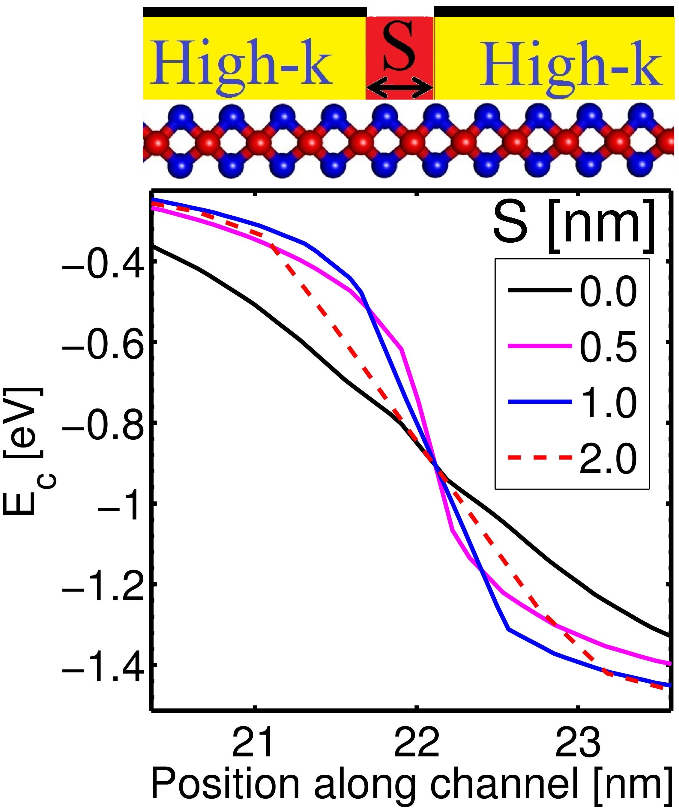
Fig. 3a shows the conduction band profile for a WTe2 DE-TFET with different spacing values. The lower the spacing, the higher is the electric field. However, this does not always translate into better performance. For example, a spacing of 0.5nm has a larger electric field compared to the spacing of 1.0nm but the energy window with high electric field of case is smaller than that of .
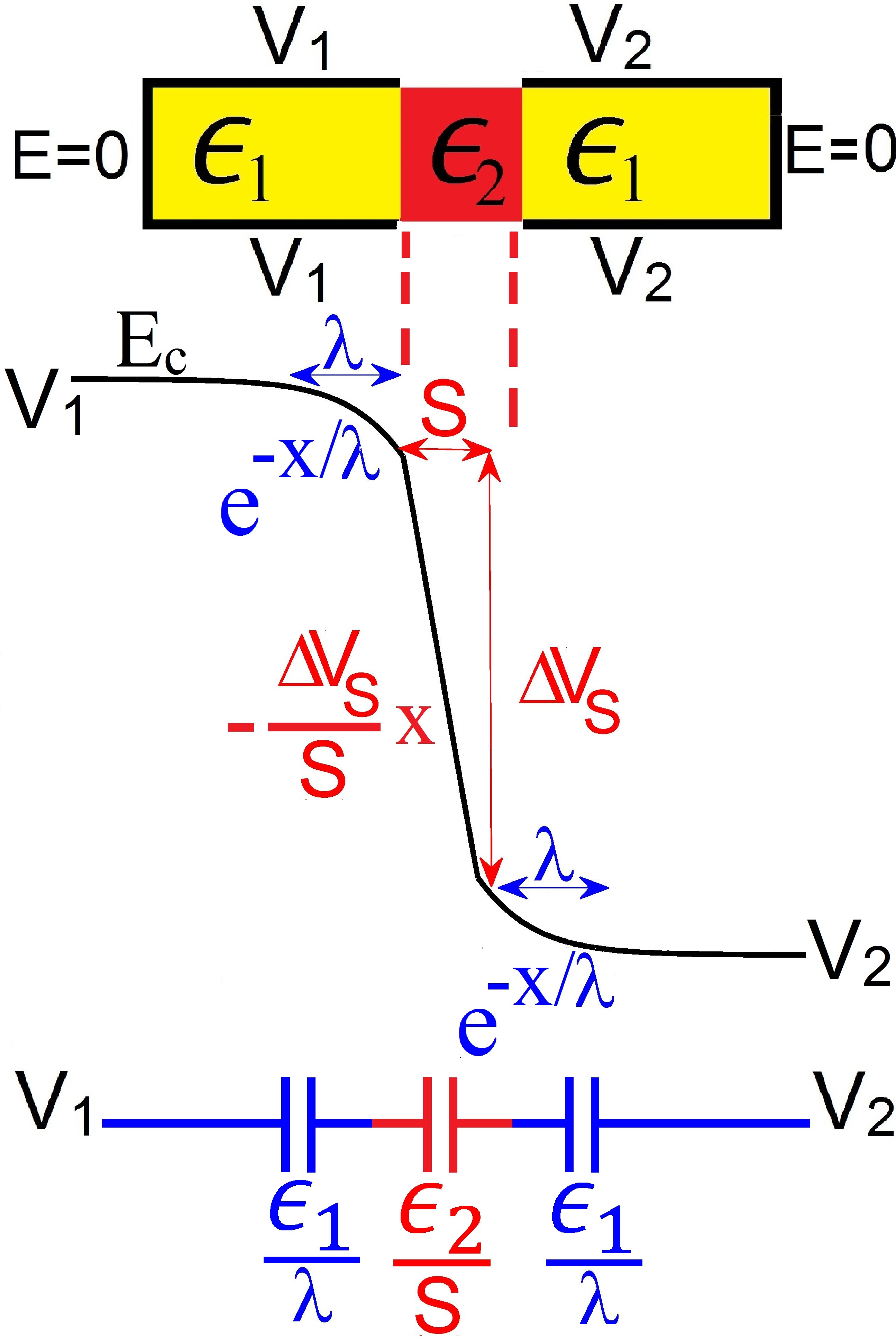
To understand the impact of low-k spacing on the potential profile and performance, an analytic model is developed. For the case of , it was previously proven that the potential can be described by a dependence with [6]. For the sake of simplicity, the channel thickness is assumed to be 0 first (). Later on, an empirical term is added to include the impact of . Simulations reveal that in the case of DE-TFETs, the potential is linear within the low-k dielectric as shown in Fig. 3b. Accordingly, the potential profile can be approximated as:
|
|
(2) |
Here, is the potential drop across the low-k dielectric and is the position of the center of the low-k dielectric. To determine , a capacitor network is used as shown in Fig. 3b.
| (3) |
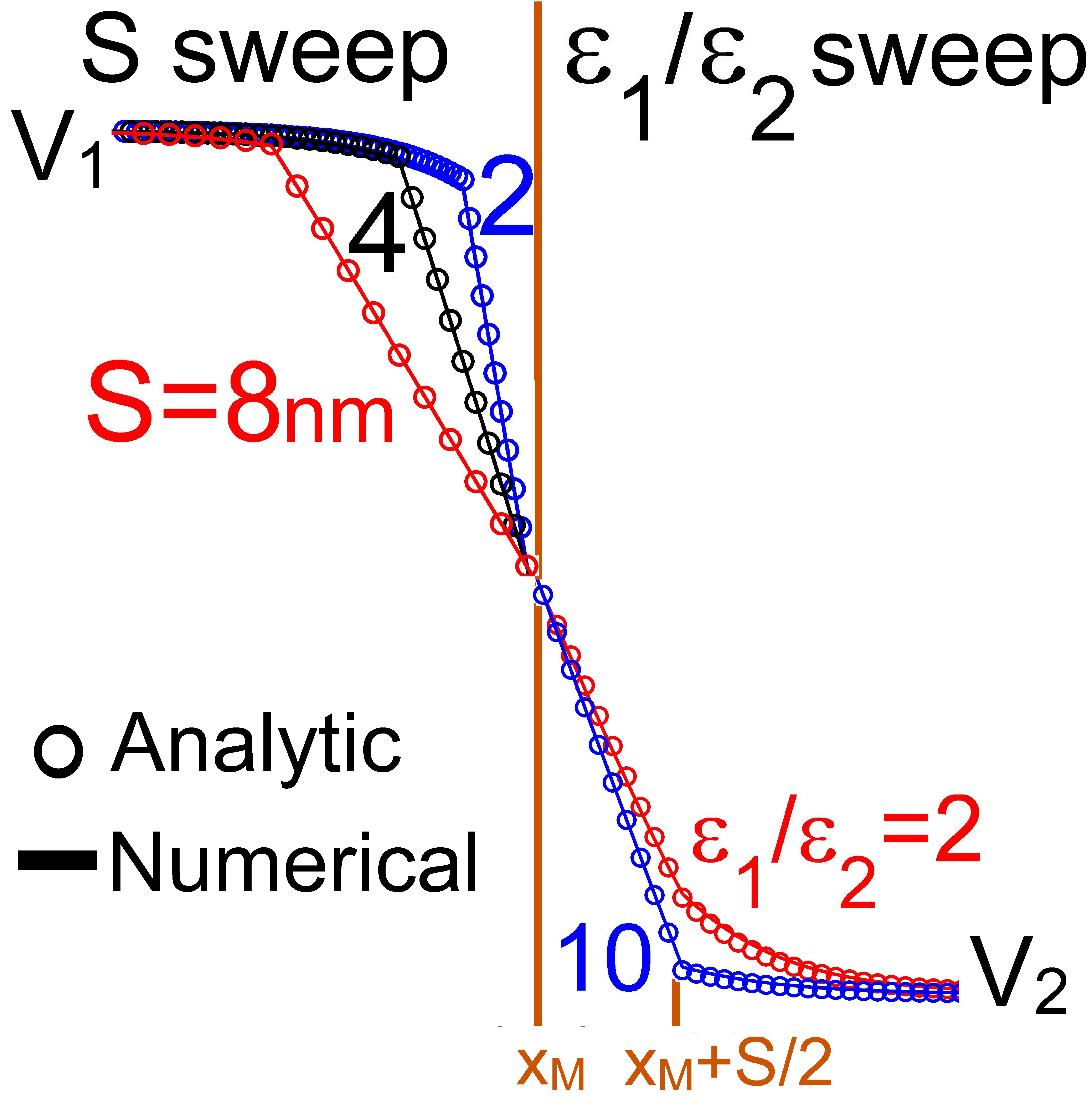
where is an empirical term to include the impact of the channel (). Fig. 3c compares the analytic potential using (2) and (3) with the numerical solution of the 2D Poisson equation which shows that the analytic solution captures the effect of the low-k spacing and the ratio of dielectric constants () accurately. The maximum performance as a function of occurs when becomes a significant portion of the total band bending ().
| (4) |
Fig. 3d depicts the optimum spacing () for the best performance of WTe2 and WSe2 DE-TFETs. Notice that does not depend on the material significantly.
V Conclusion
In summary, a new high performance TFET is proposed with a simulated record ON-current of 1000 uA/um and SS of 16 mV/dec. The high performance and high electric field in DE-TFETs is a result of the combination of low-k and high-k dielectrics. Moreover, DE-TFETs offer other advantages: e.g. smaller sensitivity to the oxide thickness compared to conventional ED-TFETs. The same idea can be applied to other device structures (e.g. nanowire TFETs) and other channel materials (e.g. III-V materials) to bring the ON-current of TFETs on par with MOSFETs and keep their excellent OFF-state performance intact.
References
- [1] J. Appenzeller, Y.-M. Lin, J. Knoch, and Ph. Avouris, ”Band-to-band tunneling in carbon nanotube field-effect transistors,” Phys. Rev. Lett., vol. 93, no. 19, pp. 196805 (2004).
- [2] M. Salmani-Jelodar, S. Mehrotra, H. Ilatikhameneh, and G. Klimeck, ”Design Guidelines for Sub-12 nm Nanowire MOSFETs,” IEEE Trans. on Nanotechnology, vol. 14, no. 2, pp. 210-213 (2015).
- [3] W. Li, S. Sharmin, H. Ilatikhameneh, R. Rahman, Y. Lu, J. Wang et al., ”Polarization-Engineered III-Nitride Heterojunction Tunnel Field-Effect Transistors,” IEEE JxCDC, DOI: 10.1109/JXCDC.2015.2426433.
- [4] H. Ilatikhameneh, Y. Tan, B. Novakovic, G. Klimeck, R. Rahman, J. Appenzeller, ”Tunnel Field-Effect Transistors in 2D Transition Metal Dichalcogenide Materials,” IEEE JxCDC (2015), DOI: 10.1109/JXCDC.2015.2423096.
- [5] G. Fiori, F. Bonaccorso et al. ”Electronics based on two-dimensional materials,” Nature nanotechnology, vol. 9, no. 10, pp. 768-779 (2014).
- [6] H. Ilatikhameneh, G. Klimeck, J. Appenzeller, and R. Rahman, ”Scaling Theory of Electrically Doped 2D Transistors,” IEEE EDL, vol. 36, no. 7, pp. 726-728 (2015).
- [7] S. Agarwal, and E. Yablonovitch, ”Band-Edge Steepness Obtained From Esaki/Backward Diode Current–Voltage Characteristics,” IEEE Transaction on Electron Devices, vol. 61, no. 5, pp. 1488-1493 (2014).
- [8] J. E. Fonseca et al., ”Efficient and realistic device modeling from atomic detail to the nanoscale,” JCEL, vol. 12, pp. 592-600 (2013).
- [9] H. Lu, and A. Seabaugh, ”Tunnel Field-Effect transistors: state-of-the-art,” IEEE EDS, vol. 2.4, pp. 44-49 (2014).