Carrier mobility modeling in highly inhomogeneous semiconductors
Abstract
The large scale various shapes and orientation defects influence into carrier scattering was theoretically analyzed using Monte Carlo method and compared to the experimental measurements. It was shown how the large scale defects screen themselves from the interaction with free charge carriers. The comparison of quantum and classical transport regimes was performed.
pacs:
72.20.My; 72.20.Dp; 72.20.JvI Introduction
One of the most important parameter describing semiconductor material is the carrier mobility. It is directly related to the speed of electronic devices made from that material. The mobility gives information about the crystal quality of the material, amount of impurity or other defects. The widely used mobility measurement methods like Hall, magnetoresistivity, time-of-flight or others enables to find the mobility values mostly in homogeneous materials, however they are often applied for the highly inhomogeneous ones. The properties of such materials usually are difficult to describe because they contain separate regions of the materials with different properties, which do not manifest as simple average. These materials are more similar to metamaterials, which distinguish global from local characteristics. As an example of this manifestation can be a conductive wire surrounded by electrical isolator. Thus the mobility in the wire can be measured, but not in the isolator, which may have high mobility but low density of charge carriers. In such samples the electrical screening or short-cutting may disable mobility calculations from Hall effect at all, like in key-1 , where neutron irradiation introduced clusters of p-type point defects into n-type crystals. However, this was not the case of carrier scattering peculiarities. The carrier mobility in these experiments was extracted from the simultaneously measured magnetoresistivity effect, showing the irradiation unaffected crystal parts, which had high carrier mobility. Very similar behavior of these two mobility measurements also were observed in samples after the defect engineering key-2 or self formation of oriented large scale defects key-3 ; key-4 . In both cases the Hall voltage signal was anomalously low and the magnetoresistivity effect was distinctly sensitive to the orientation of the samples. The effect was not attributed to the change of the carrier scattering. It was thought the effect rises from the measurement particularity but not the carrier transport. Thus in the presence of such kind large-scale defects the question was unanswered: when the measurement results describing scattering processes can be distinguished from the measurement peculiarities with partial incompatibility? To answer this question, the modeling was performed with similar geometry defects in the scope of quantum and classical transport mechanisms with Monte Carlo method. The method was chosen because of implementation simplicity and the availability of large computing resources. Several types large scale defects were used for the carrier scattering investigations. The supplemental research was performed as experimental modeling for the certain large-scale defect configurations.
II The Theory Background
From the point of view of Monte Carlo method, the transport of carriers in the crystal may be found by repeating the steps of a single carrier walk and making the statistical average. The first assumption was made that the carriers do not interfere between themselves. Then the classical diffusion transport principles may be applied. In that case the mobility of the particle is directly proportional to the diffusion coefficient by Einstein relation . The diffusion of the particle is considered as random walk in the crystal and the collision events occur with phonons and crystal structure irregularities. The phonons at each time step appear randomly and in the modelling they are considered as determining random direction for the next step. Thus, the temperature is not included in this model other way and its absolute value is not calculated. The mobility is reciprocally proportional to the number of the scattering events and we will consider the mobility only qualitatively. The screening of the internal potential by free carriers is not included, so the model is limited to be suitable for higher resistivity materials. The crystal structure defects may be treated as particle scattering centres with the finite interaction probability. In mesoscopic transport systems the particle transfer through the defective region may be described using Landauer model key-5 , which introduces the transfer coefficient T. The crystal field distortion caused by defects may be considered as barriers or wells in the paths of the quasi-free charge carriers. For the simplicity, in our modelling the shape of the distortions were approximated as bar-shape profiles. Thus the defects were treated as rectangular potential barriers as shown in Figure 1.
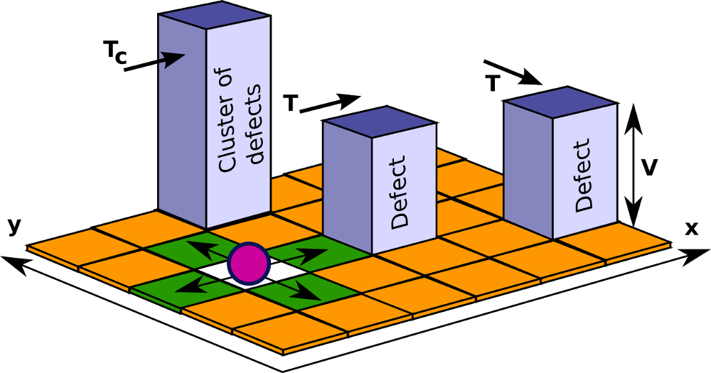
The classical transport through the barrier states that the particle may jump it over only if it has the energy greater than the potential energy of the barrier. Or else the particle is reflected completely. In quantum mechanics the probability of the particle to penetrate through the finite size barrier is always greater than zero:
| (1) |
here is the potential height in energy units, is the particle energy, is the width of the barrier in space units, is an impulse parameter , relating particle mass with energy parameters and fundamental constant. The particle dispersion was limited to its ability to perform only one constant space step and the fundamental constants were chosen appropriate . The reflection probability is . The infinite size of the barrier gives the same result for the classical or quantum transport through the barrier. The modelling was performed only for 2 dimensional space grid (size 1500 x 1500 points) as it is less time consuming than 3D but gives qualitatively good results. The particle motion on the grid was available only in 4 directions. It was enough to have possibility for stepping over all space points and every step may be treated as one dimensional, this enabled simple evaluation of T for the next step. The step was fixed to the length of the single space point. The defects were treated either as neutral or screened to the size of the single space point. Initially the space was randomly filled with the number of point defects acting as background scatters. Further, more point defects were placed in certain arrangements to create larger scale defects. The particle for the modelling was randomly placed in the space at the grid point without defect and counted steps for each arrangement. The translational symmetry boundary conditions were applied to keep the particle in space. The potential of the single defect was assigned to be 10 times grater than the energy of the jumping particle. So the cluster potential may be several times greater than for the single defect. In this case the particle energy corresponds to real transition probability or low temperature of the system.
III Point Defects And Clusters
When the crystal contains plenty of the point defects, their characterization (detection) may be difficult because of their fields overlap and clusterization. Starting with the model of randomly distributed point defects we may observe that increasing the number of the scattering centres (point defects) not linearly increases the number of the scattering events as shown in Figure 2.
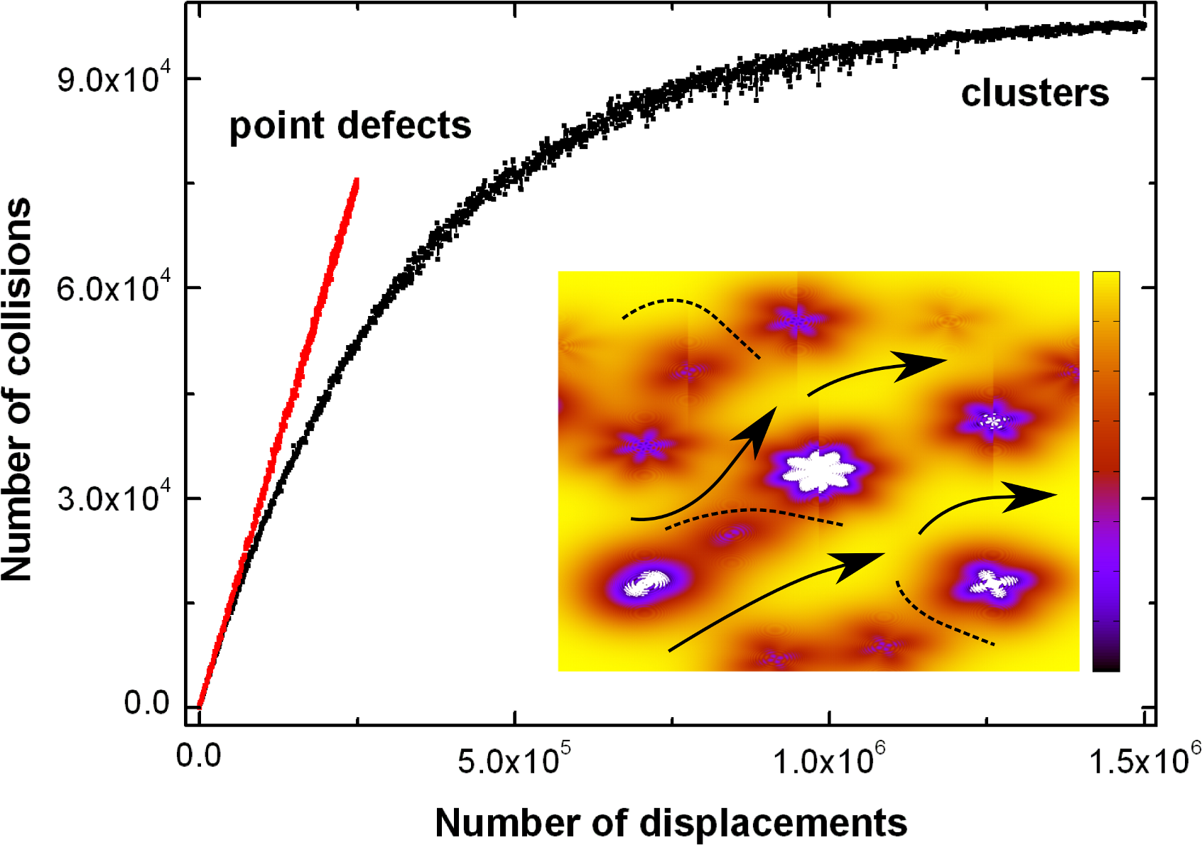
Here the linear dependence corresponds to point defects. It was obtained by putting only single defects at sites on the space grid. The defective sites were allowed to appear in the neighbourhood, still their conglomerations were not influencing as clusters. In contrast, the other dependency is saturating, which indicates the presence of clusters. The illustration in the Figure 2 shows the paths of the charge carriers around large scale defects (or clusters), which do not allow the carriers to penetrate into some regions. Electrical characterization of such material is complicated because the part of it is isolated while the rest of it may still be of good quality. The electrical resistivity of such material can be fairly measured but the carrier mobility measurements may return failures. The clusters of only few point defects may be considered as single scattering centres with larger interaction cross-section because the electric field smoothers the edges of the branchy structures.
IV Some Large Scale Deffect Geometries
Further geometries of this investigation are shown in Fig. 3. Here the orientation of the defects (samples) to the external electric voltage is important. The parts of the figures correspond to the crystal samples with the electric potential driving carriers along the samples length. The external voltage in the modeling is included into the particle jump probability as additive parameter to the defect barrier potential in one direction (x) and as additional jump direction choice (x) for the 4 possible random directions (x, -x, y, -y) where the barriers are absent. The parts (a) and (b) in Figure 3
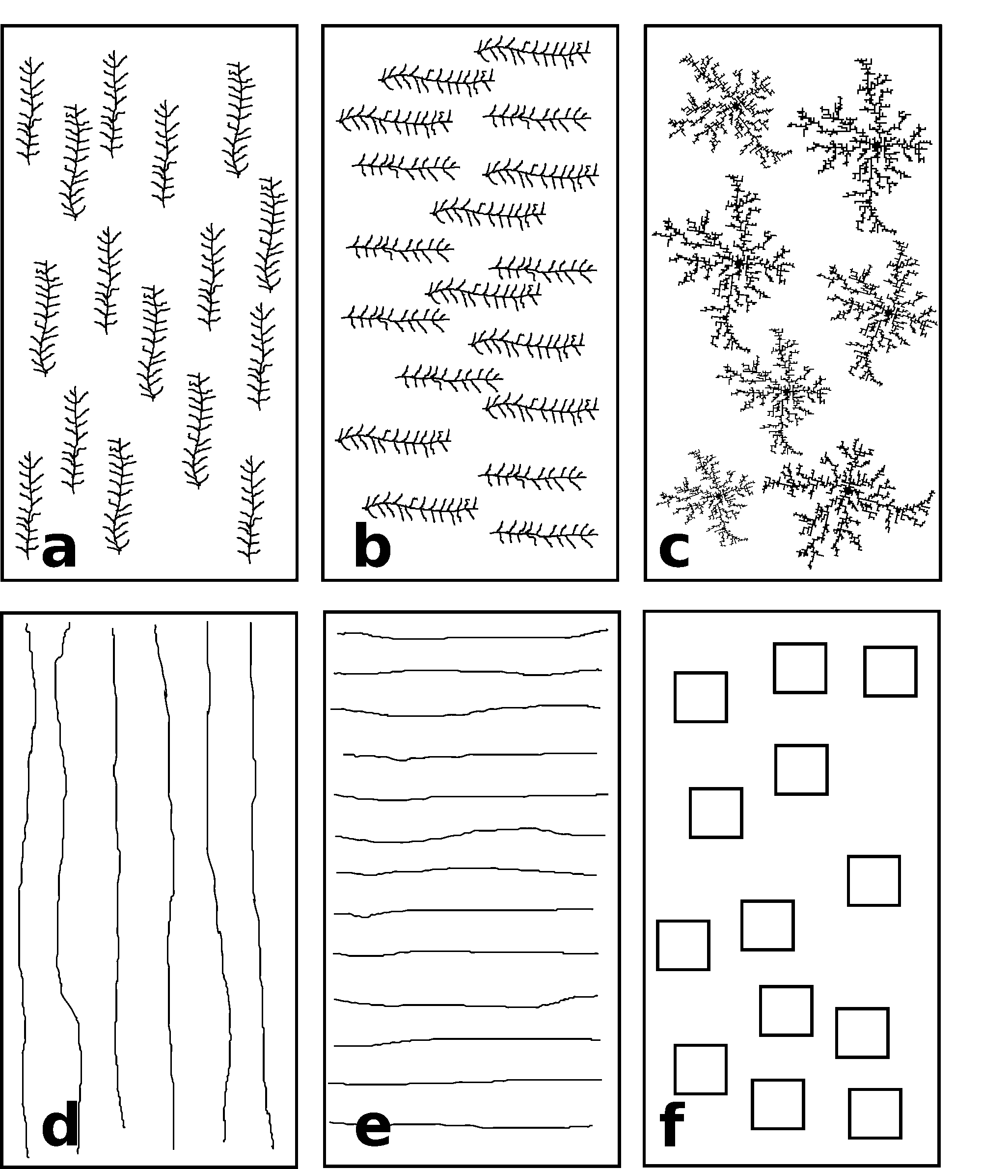
sketch the pattern of defects obtained in the 3C-SiC crystals key-3 ; key-4 (cubic lattice silicon carbide). These defects are the twin boundaries (TBs) in a shape of fir tree branch. The magnetoresistant mobility in these samples differs times depending on the orientation of the samples. Experimentally only two orientations were measured as shown in Figure 3. Here the scattering modeling was applied for these two orientations including the transformations from one to another. The results are presented in Figure 4. The upper part of this figure corresponds to the quantum transport. In the middle of the figure the orientation of the defects (sample) is displayed. As one can notice, the zero angle (with the period of 180 degrees) gives the greatest scattering, while for the 90 degrees (with the period) the scattering is lower. Depending on the number of the large scale defects, the scattering difference on the rotation angle becomes more distinct. The fir tree pattern of the defects acts as carrier trap for the further scattering. In the quantum transport regime if the particle once jumped over the barrier it is more probable it will go away from the defect because of being dragged by the external field. However in the classical regime, the particle may only walk around the defect and the external field returns the particle back into the defect of the complex structure. The lower part of the Figure 4
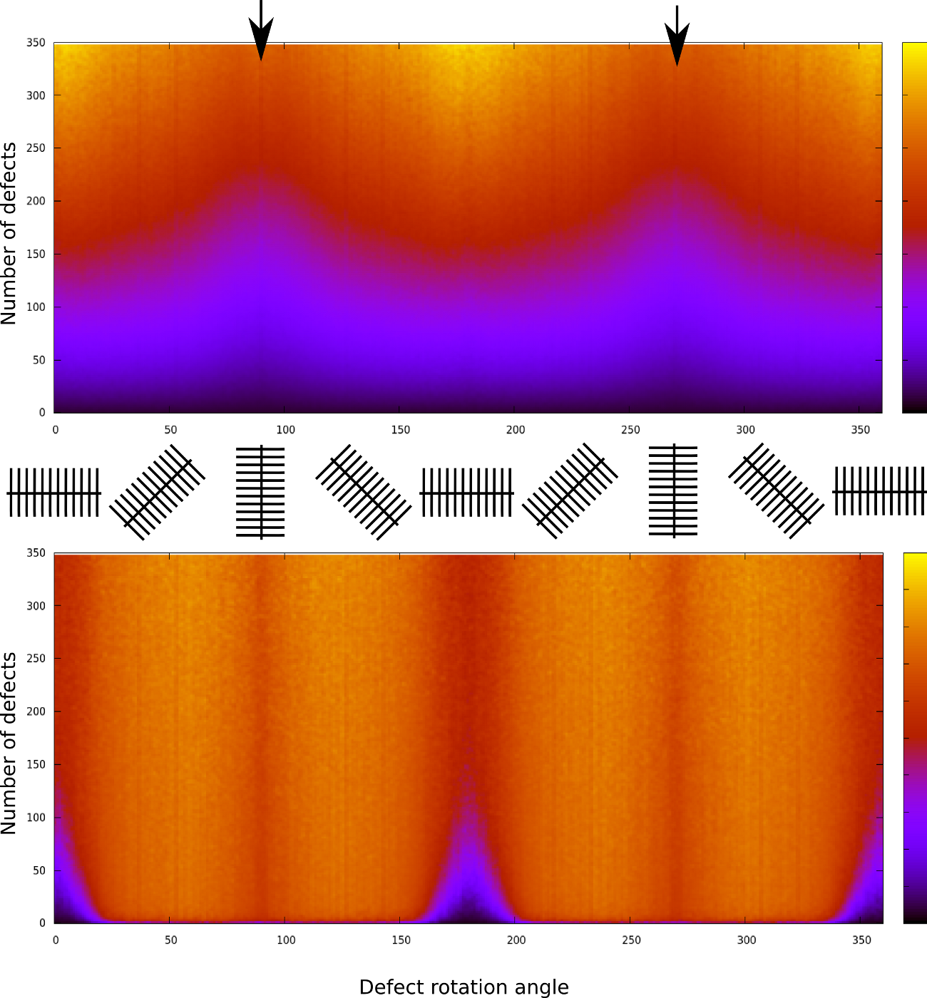
shows clear difference between these transport regimes. The classical one has the greatest scattering at the angles where the quantum one has the lowest. The exception is marked by the arrows where the both regimes have minima. This result of the different scattering behavior is not trivial. In reality the barriers of the large scale defects may be high enough to be treated as infinite (classical), but when the defect “captures” the carrier its electric charge repulses other carriers away and statistically the effective number of scatters changes. The described classical transport may take place only when the carrier density is low and the carriers do not interfere each other. Comparing the modeling results with the experiment it may be stated that the TBs in 3C-SiC should be treated quantum mechanically in the carrier transport analysis.
The other experimentally measured sample with oriented defects is shown in Figure 3 (d) and (e) parts key-2 . These large scale defects were created by scratching the SiC crystal substrate in lines then the 3C-SiC phase was grown on top and the substrate removed. The boundaries between the 3C phase material parts penetrated through the whole crystal. The idea of this scratching was to release the strain of the overgrown layer and avoid cracks. The good quality of the crystals between the inner boundaries was obtained but the carrier transport through the whole crystal was greatly modified. Here the good agreement of the experiment with the theory was found. The defects along the sample contribute as more effective scatters that the perpendicular ones. The modeling of only quantum regime was analyzed because the perpendicular classical defects isolate the material completely. The summary of these and some more defects (from the Figure 3) contribution for the carrier scattering is shown in Figure 5.
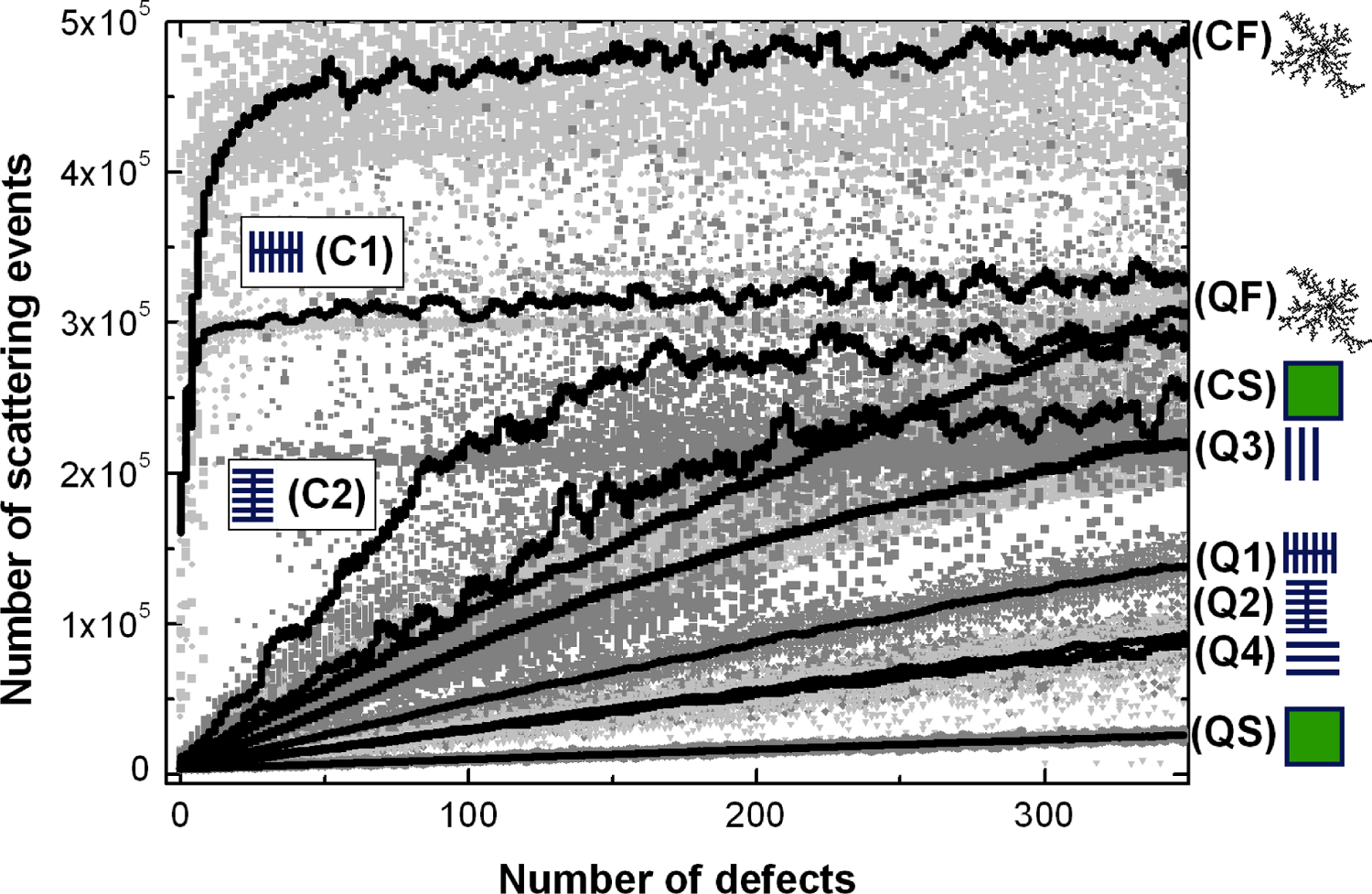
At the right of the figure the defect forms are drawn and the names are marked for quantum (with letter Q) and classical (C) regime. The classical scattering is always greater comparing to the quantum one for the same type of the defects. The growth of the number of the scattering events grows nonlinearly with the number of defects indicating the defect self screening effect. It is mostly expressed in the classical transport, in which the number of the scattering events rapidly grows to the saturation values. This case can be attributed to the material with isolating inclusions, which do not influence scattering. By comparing the types of the defects one can notice that the screening is most significant in fractal type defects (Figure 3 c) or fir tree-like defects perpendicular to the external field (Figure 3 b). The similar to fractal defect structure may be found in crystals with cracks or electrical break through. Also the high energy irradiation of heavy particles may be followed by cascade displacement events when point defect tracks are created, which shape is close to shown in Figure 3c. These kind defects effectively screen the crystal volume from the charge carriers like was shown in key-1 . The lowest contribution to the scattering is found for the square shape defects in quantum regime (Figure 5, QS) and is similar to the form described in key-6 ; key-7 ; key-8 for the Hall effect. In classical regime their contribution is comparable to the other defect forms. This is explained as the total screening of the interior of the large defect in the classical regime. In case of the square defects (they are empty inside) the quantum transport senses only their boundary and background point defect scattering. Thus the number of active point defects is lower comparing to the other defect shapes. The size of each sort large scale defect was chosen to be of the similar space volume. This fact does not restrict analysis to the single size of the defects but makes them comparable between the sorts.
V Experimental Modeling
To improve the analysis of the mentioned defects influence to the charge transport parameters the experimental modeling was performed on thin semiconducting layers. The layers produced by Physical Vapor Deposition technique, which details are not important here. The semiconductor material was chosen for convenience and ability was PbTe, which has fair high carrier mobility and consequently produces higher Hall voltage. In our experiment the layer formation conditions were such that the highest Hall mobility was found about 750 . For the defect modeling two types of the defects with two perpendicular orientations were used as shown in Figure 6.
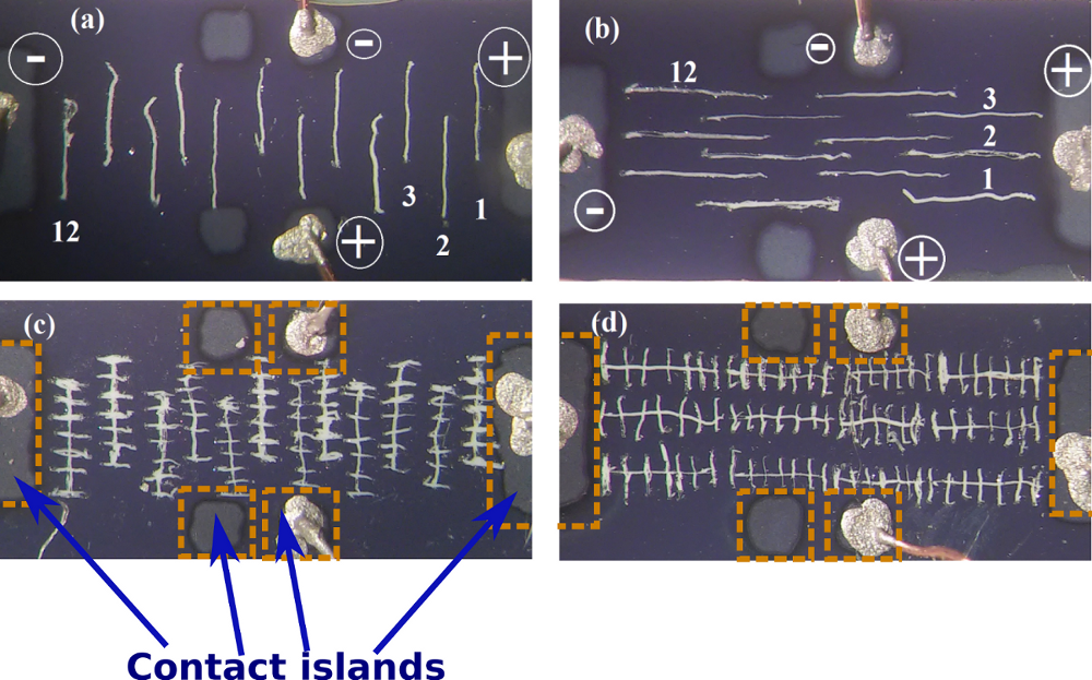
Here four samples are shown with planar electrical contacts of Hall bar-shape configuration and the scratched surfaces with intention to repeat defect configuration from Figure 3 d, e, a, b parts respectively. The scratches were done by metallic needle in the numbered order shown on the photographs. After each large-scale defect formation, Hall and magnetoresistivity measurements were performed at room temperature to obtain carrier mobility. The experimental results are shown in Figure 7.
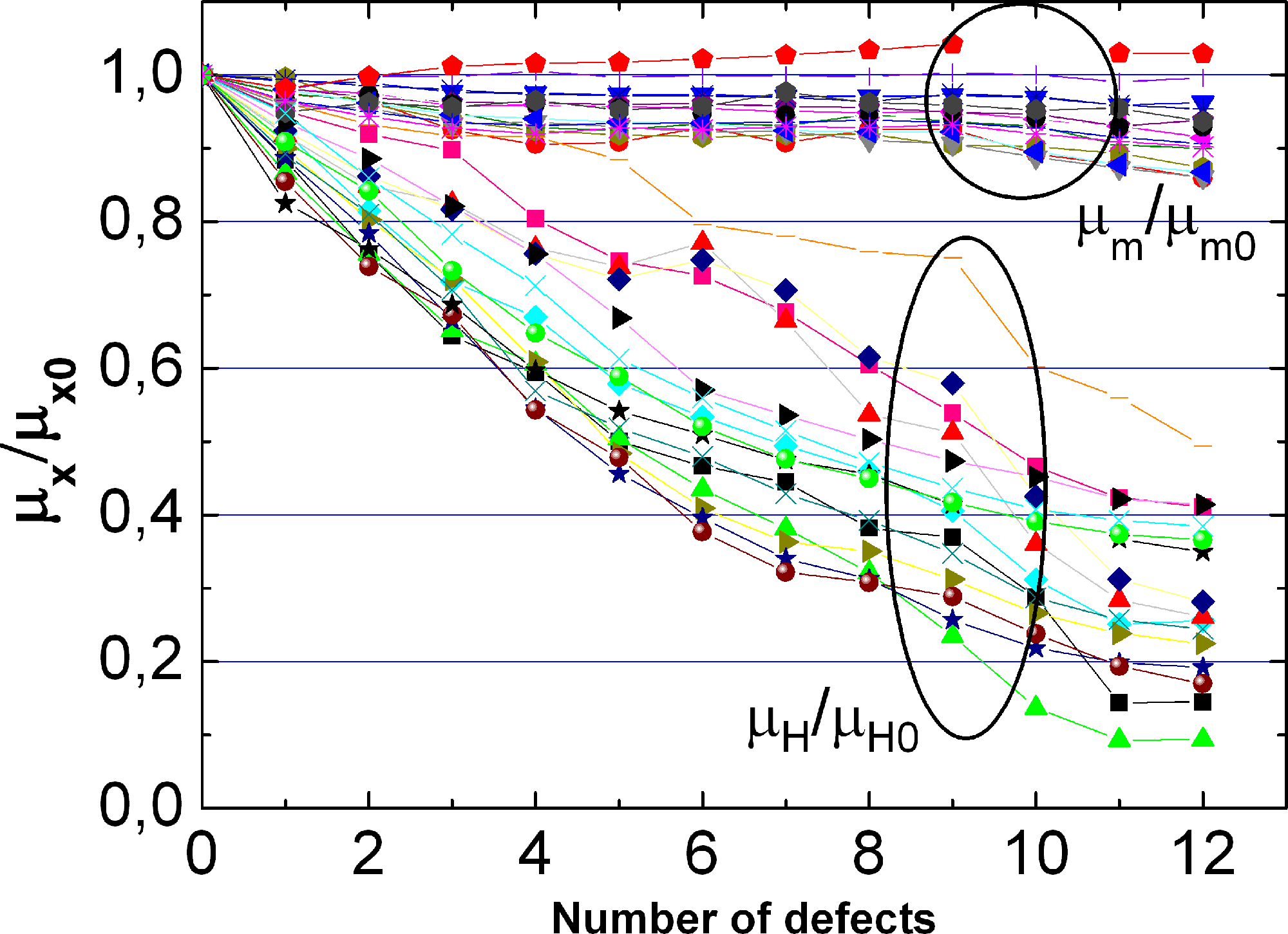
Here the relative mobility dependence on the number of scratched defects is plotted for all samples and appear more like statistical variation. The most distinguishing result is that Hall mobility signal (lower curves in the figure grouped by an oval shape) is much more sensitive to the appearance of the defects than magnetoresistant mobility (upper curves). The similar result was observed in for the silicon irradiated by neutrons key-1 or electrons key-9 . The difference of magnetoresitant mobility values for the fir-tree like defects orientation (shown in Figure 6 c) and d) parts) was expected to be the most expressed like in 3C-SiC case, however the experiment showed that magnetoresistant mobility is not sensitive to this kind defect orientation. The explanation may be that size of the structural parts (perpendicular scratches) of the large scale defect does not differ enough from the total size of the defect. In case of line-shape defects (Figure 6 a) and b) parts) the most interesting observation is the increase of mangetoresistivity in certain sample when defects are perpendicularly oriented to the average electric current flow direction (Figure 6a). This result is in agreement with the one found in 3C-SiC key-2 . The influence of the defect shape and orientation in the current experiment may be better observed for dependency on resistivity as shown in Figure 8.
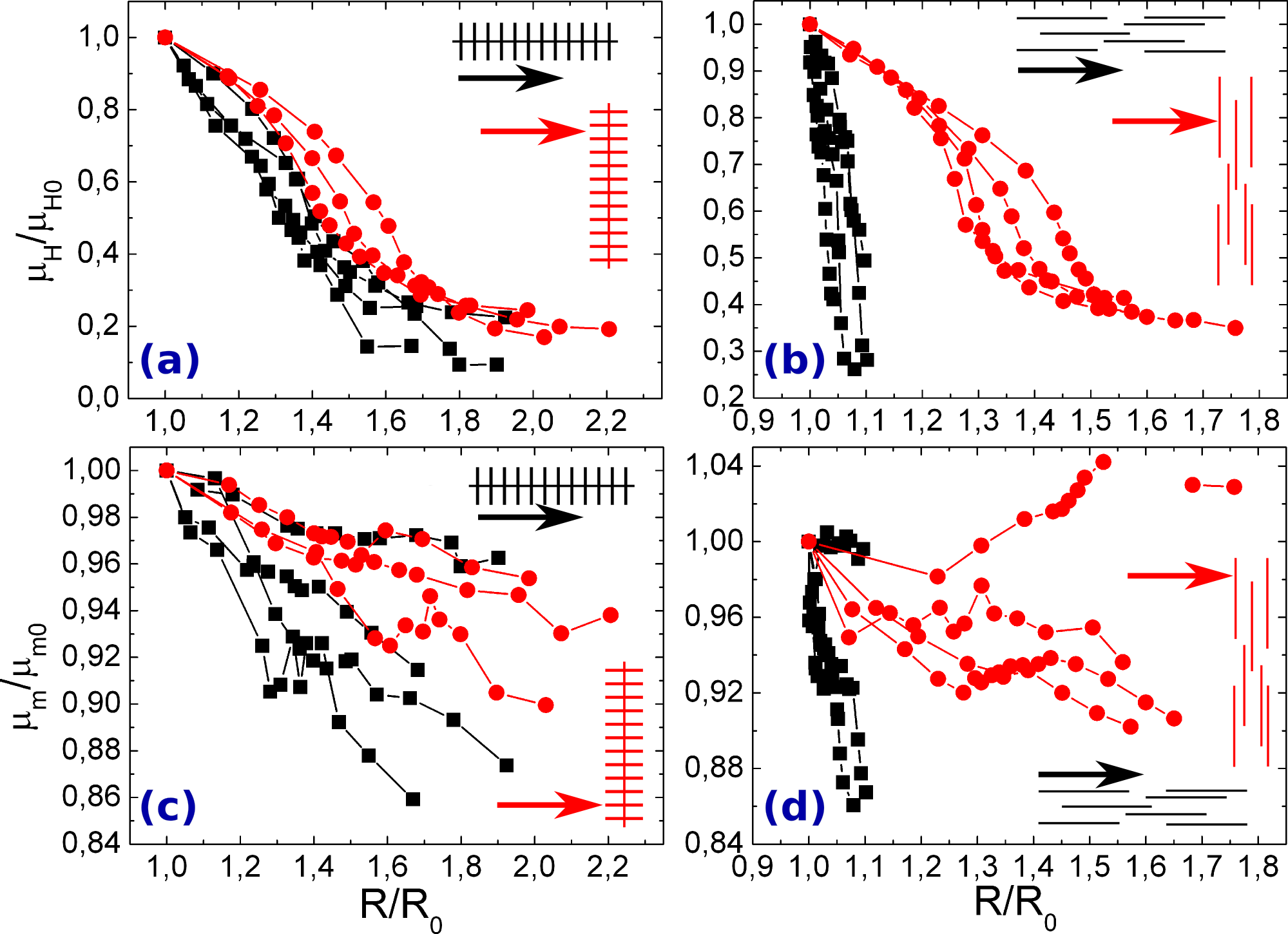
The relation between resistivity and mobility may give information about the charge carrier density. In this case that relation is not straightforward and is affected by the geometry of the defect. One can notice that in case of line-shape defects (Figure 8 b), the Hall mobility drops much faster with resistivity when the defects are along the electric current and perpendicular to the Hall field. The resistivity in this case cannot change much because the defect lines separate the sample into array of parallel resistors. However Hall voltage is created much smaller because the carriers reach the Hall contacts through the field of obstacles. The same effect is observed in magnetoresistivity (Figure 8 d), when line-shape defects do not allow carriers to bend in magnetic field and increase their path. The opposite effect, when magnetoresitivity is increased, is observed in the case when the same type defects are oriented perpendicularly to the electric current path (Figure 8 d red dots). In this case magnetic field turns the carriers into the regions around defects, which effectively increase the paths.
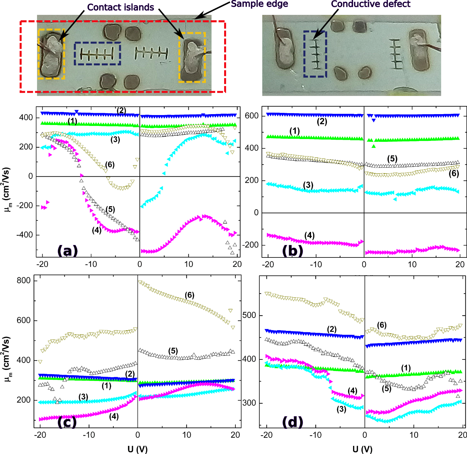
The defects shown in Figure 6 are electrical insulators (at least in the bulk). It is reasonable to investigate the influence of the same type defects to the electrical parameters when the defects are electrical conductors. For this purpose the same material (PbTe) was evaporated in vacuum with aluminium as shown in Figure 9 photographs. The size of the defects is of the order for consideration about only electrical potential redistribution but not the scattering of the charge carriers. In this case the orientation of the defect is less important as one can nottice its influence to the magnetoresistivity. In the figure the magnetoresistant mobility is calculated as the square root of magnetoresistivity divided by magnetic field induction and the sign extracted out from the root. When the defects are absent the magnetoresistivity is proportional to the drift mobility with certain geometry factor and it is independent on the applied electric voltage (plots 1 and 2) as it should be. When only one defect is manufactured the magnetoresistivity drops in all cases while even in some it becomes negative (plots 3 and 4). The negative magnetoresistivity may be explained by more conductive edges of the semiconductor layer when the carriers are turned by magnetic field to these edges. It has to be noted that the voltamperic characteristics are linear in all cases and the resistivity is only slightly affected by the presence of the defect. Since the artificial defect is formed from metal on semiconductor the junction barrier should be present. The semiconductor layer below the metal is not intacted, so the free carriers are influenced in these regions only by potential redistribution, which may be considered as a bunch of low barriers. In that point of view the scattering of the free carriers may be also considered. The evaporation of the second defect may be expected to enhance the described effect, however in all cases it acts in the opposite manner: the magnetoresistivity is increased and in some regions it is greater than the initial (for example part c, positive voltage graphs 5 and 6 comparing to 1 and 2). It is similar to the case for the defects shown in Figure 8 part (d) when the defects are perpendicular to the electric current direction. This fact suggests that the increase of the magnetoresistivity is more related to the defect which is repulsive (or isolating) to the charge carriers. The influence of the defect orientation in this case is observed in voltamperic characteristics. When the defect is as shown in Figure 9 at the left photograph, the resistivity after the formation of the first defect increases while the second defect slightly decreases the resistivity in comparison to the previuous one. For the another orientation the resistivity constantly increases with the number of defects. Since the doping was constant in all cases the conductivity may change only with carrier mobility, which is not proportional to the magnetoresistivity any more.
VI Summary
The material characterization by mobility measurements reveals the number of scattering centers, which may be not exact because the large-scale defects may demonstrate self-screening effect. The complete and reliable analysis requires a set of investigations with different numbers of defects because their influence is not straight-forward for the extrapolation. In some cases these numbers may be changed with intense light excitation, when non-equilibrium charge carriers change the profiles of the defect potentials. The shape and orientation of the large-scale defects may play a significant role in carrier transport and the structural characterization has to be performed before making conclusions from the electrical measurements.
ACKNOWLEDGEMENTS
The authors would like to thank prof. J. V. Vaitkus from Vilnius University for suggestions and recommendations preparing this work. L. Andrulionis is grateful to the Institute of Applied Research for support with “Viscakas” stipend. The support from Research Council of Lithuanian is also acknowledged (Grand No. MIP-15200).
References
- (1) J.Vaitkus, A.Mekys, J.Storasta. Analysis of microinhomogeneity of irradiated Si by Hall and magnetoresistance effects. 10th RD50 Workshop on Radiation hard semiconductor devices for very high luminosity colliders. Vilnius, 2007.
- (2) P. čajev, A. Mekys, P. Malinovskis, J. Storasta, M. Kato, and K. Jara iūnas. Electrical parameters of bulk 3C-SiC crystals determined by Hall effect, magnetoresistivity, and contactless time-resolved optical techniques. Materials Science Forum Vols. 679-680 (2011) 157-160. doi:10.4028/www.scientific.net/MSF.679-680.157.
- (3) R. Vasiliauskas, A. Mekys, P. Malinovskis, M. Syvajarvi, J. Storasta, R. Yakimova, Influence of twin boundary orientation on magnetoresistivity effect in free standing 3C–SiC , Materials Letters 74 (2012) 203.
- (4) R Vasiliauskas, A Mekys, P Malinovskis, S Juillaguet, M Syvajarvi, J Storasta and R Yakimova Impact of extended defects on Hall and magnetoresistivity effects in cubic silicon carbide., J. Phys. D: Appl. Phys. 45 (2012) 225102.
- (5) S. Data. Electronic Transport in Mesoscopic Systems. Cambridge University Press (1997) 369.
- (6) R. H. Bube. Interpretation Of Hall And Photo-Hall Effects In Inhomogeneous Materials. Appl. Phys. Lett. 13 (1968) 136.
- (7) J. Viscakas, K. Lipskis, A. Sakalas. On the interpretation of Hall and thermoelectric effects in polycrystalline films. Lith. Jour. Phys. 5 (1971) 799-806.
- (8) W.Siegel, S Schulte, G. K hnel, J. Monecke. Hall mobility lowering in undoped n-type bulk GaAs due to cellular-structure related nonuniformities. J. Appl. Phys. 81 (1997) 3155.
- (9) A. Mekys, V. Rumbauskas, J. Storasta, L. Makarenko, J. V. Vaitkus. Defect analysis in fast electron irradiated silicon by Hall and magnetoresistivity means., Nuclear Instruments and Methods in Physics Research Section B 338 (2014) 95.