Conductance, Valley and Spin polarization and Tunnelling magneto-resistance in ferromagneticnormalferromagnetic junctions of silicene
Abstract
We investigate charge conductance and spin and valley polarization along with the tunnelling magneto-resistance (TMR) in silicene junctions composed of normal silicene and ferromagnetic silicene. We show distinct features of the conductances for parallel and anti-parallel spin configurations and the TMR, as the ferromagneticnormalferromagnetic (FNF) junction is tuned by an external electric field. We analyse the behavior of the charge conductance and valley and spin polarizations in terms of the independent conductances of the different spins at the two valleys and the band structure of ferromagnetic silicene and show how the conductances are affected by the vanishing of the propagating states at one or the other valley. In particular, unlike in graphene, the band structure at the two valleys are independently affected by the spin in the ferromagnetic regions and lead to non-zero, and in certain parameter regimes, pure valley and spin polarizations, which can be tuned by the external electric field. We also investigate the oscillatory behavior of the TMR with respect to the strength of the barrier potential (both spin-independent and spin-dependent barriers) in the normal silicene region and note that in some parameter regimes, the TMR can even go from positive to negative values, as a function of the external electric field.
pacs:
73.23.-b, 73.63.-b, 72.80.Vp, 75.76.+jI Introduction
A close cousin of graphene, silicene has been attracting a lot of attention in recent times both theoretically and experimentally Ezawa (2015); Lalmi et al. (2010); Padova et al (2010); Vogt et al. (2012), due to the possibility of new applications, given its compatibility with silicon based electronics. Although earlier theoretical analyses Liu et al. (2011a); Ezawa (2013a, b) had predicted the possibility of silicene and even germanene, stanene, etc, interest in this subject rose after experimentalists observed hexagonal structure in silicene sheets deposited on a silver substrate Lalmi et al. (2010); Padova et al (2010); Vogt et al. (2012). Unlike graphene, silicene does not have a planar structure; instead it forms a buckled structure due to the large atomic radius of silicon, resulting in a band gap at the Dirac point Liu et al. (2011a). Further, it turns out that such a band gap is tunable by an external electric field applied perpendicular to the silicene sheet Drummond et al. (2012); Ezawa (2013b). Thus, from the point of view of applications, one of the drawbacks of graphene in making transistors is overcome by silicene, and very recently, a silicene based transistor has been experimentally realised Tao et al. (2014). Therefore, with the possibility of silicene based electronics, experimental interest in silicene remains quite high.
Theoretical interest in silicene soared when it was realised that one could have topologically non-trivial phases in silicene, tuned by the external electric field Drummond et al. (2012); Ezawa (2013b). Graphene and silicene have similar band structures and the low energy spectrum of both are described by the relativistic Dirac equation i.e., both have the Dirac cone band structure around the two valleys represented by the momenta and . However, in silicene, the spin-orbit coupling is much larger than in graphene Guzmán-Verri and Lew Yan Voon (2007); Liu et al. (2011a); Ezawa (2013b). This is an important difference which causes the Dirac fermions to become massive. Furthermore, because of the buckled structure in silicene, the two sub-lattices respond differently to an externally applied electric field. This means that the Dirac mass term becomes tunable Ezawa (2013b), and hence allows for the mass gap to be closed at some critical value of the electric field and then reopened. The phases on the two sides of the critical value where the gap is closed are different, with one of them being topologically trivial and the other being topologically non-trivial Ezawa (2013a, b, 2012). Hence, under suitable circumstances, silicene can be a quantum spin Hall insulator with topologically protected edge states Liu et al. (2011b); Ezawa and Nagaosa (2013).
In recent years, spin based electronics or spintronics has become a prominent field of research both theoretically and experimentally Zutić et al. (2004). The upsurge of activity in this area is essentially due to the realisation that devices based on the spin degree of freedom are almost dissipationless unlike those based on the charge degree of freedom. The possibility of using silicene as a spintronic device has been reported very recently in Ref. [Wang et al, 2015; Rachel and Ezawa, 2014; An et al., 2012; Tsai et al., 2013; Shakouri et al., 2015] due to its strong spin-orbit coupling. Another important quantity in spintronics is the tunneling magnetoresistance (TMR) which occurs at junctions between materials i.e., ferromagnetnormal metalferromagnet (FNF) junctions. The resistance of the junction is different for parallel and anti-parallel spin configurations, and this difference in resistance can be experimentally measured.
In this paper, we study charge conductance and spin and valley polarizations along with the TMR in silicene junctions, in particular the FNF junctions, as the external electric field is tuned through the system. We model our FNF setup within the scattering matrix formalism Datta (1995). A similar setup has been utilised in graphene Zou et al. (2009) to study TMR, while valley polarization has been studied in a normalferromagnetnormal (NFN) junction in silicene Yokoyama (2013). In Ref. Yokoyama, 2013, the author has investigated the conductances and valley polarization of a NFN junctions in silicene. Spin and valley textures of the particle-hole excitations due to the addition of external fields is another important issue in silicene and recently, analytical and numerical results for the dispersion of the plasmons has been studied Duppen et al. (2014). However, conductances and TMR based on silicene FNF junction have not yet been considered in the literature.
The remainder of this paper is organized as follows. In Sec. II, we present our model and band structure for the ferromagnetic silicene (FS). In Sec. III, we describe the scattering matrix for the FNF junction to compute the two terminal charge conductance (), valley and spin polarizations () and the TMR. In Sec. IV, we present our numerical results for the conductances, spin and valley polarizations and TMR in the FNF set up for various parameter regimes. Finally in Sec. V, we present the summary of our numerical results followed by the conclusions.
II Model and band structure
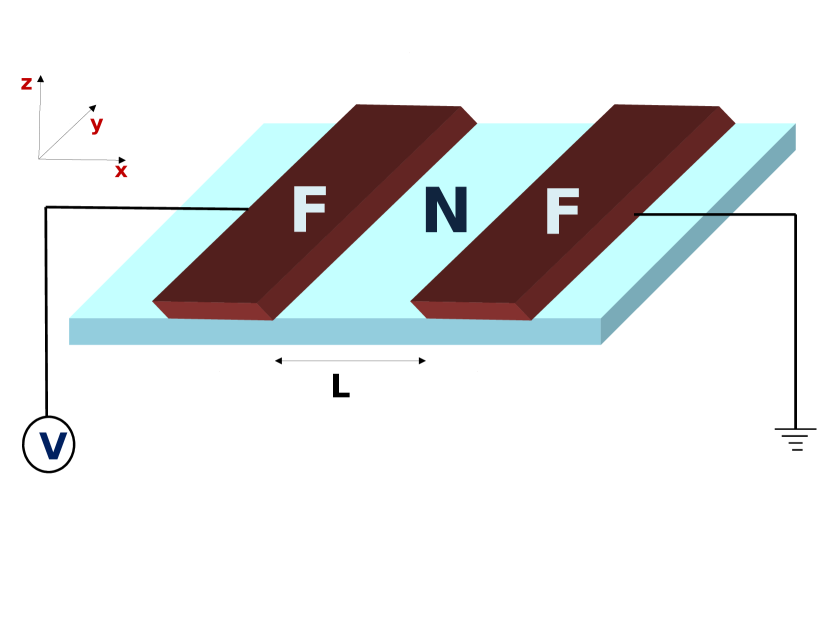
We study the FNF junction set up in silicene as shown in Fig. 1. Ferromagnetism is induced in silicene by the proximity effect when it is placed in proximity with a magnetic insulator, which we model by the following Hamiltonian given by Yokoyama (2013)
| (1) |
where is the Fermi velocity of the charge carriers in silicene, is the charge of the electron and correspond to the valley and spin indices and corresponds to the sublattice (pseudospin) Pauli matrices. is the parameter that specifies the spin-orbit coupling in silicene. Due to the buckled structure of silicene, the atoms in the two sublattices respond differently to an externally applied electric field Ezawa (2013b). Thus is the potential difference between the two sublattices A and B due to this applied electric field where is the separation between the two sublattices. Hence, the potential difference is a tunable parameter and can be tuned by an external electric field Ezawa (2013b). Also, when the Fermi energy is close to the Dirac point, at the critical electric field , one of the valleys in silicene is up-spin polarized and the other one is down-spin polarised Ezawa (2013b). Here denotes the and valleys respectively and denotes the spin indices. denotes the profile for the potential barrier in the normal silicene region and corresponds to the exchange splitting, or the energy difference between the up and down spin electrons in the FS regions. Note however, that in real materials the proximity of a ferromagnet to silicence can actually change the band structure of silicene itself. In that case, the only way to proceed will be to perform first principles calculations as have been done in graphene Yang et al. (2013).
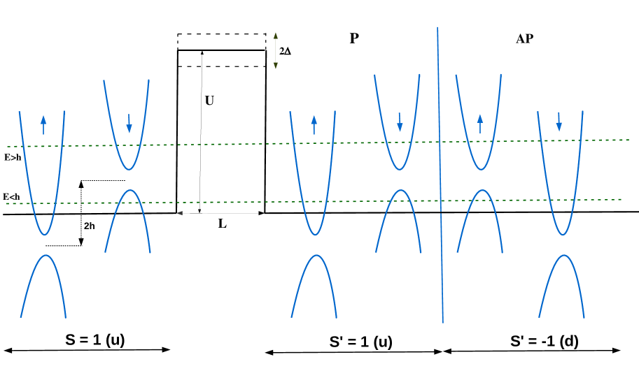
We now consider the geometry shown in Fig. 1 and assume that the system is translationally invariant along the direction. The interface between the normal and the FS are located at and where the length of the normal silicene region sandwiched between the ferromagnetic patches. Here is the profile of the potential barrier modelled in the normal silicene region and denotes the exchange field or Zeeman field in the two ferromagnetic regions with corresponding to the parallel (P) configuration and corresponding to the antiparallel (AP) spin configurations of magnetization respectively. We show the schematic of up and down spin in left region (for ) and in right region for parallel ( or P or ) and antiparallel ( or AP or ) configurations in FNF junction for both and regions in Fig. 2. The orientation of the exchange field in the left region is kept fixed by keeping and then and in the right region corresponds to the parallel (P or ) and antiparallel (AP or ) configuration respectively. Note that the line crosses the same band in the third region for the P configuration, but crosses the other band for the AP configuration. As reported earlier Zou et al. (2009), this feature gives rise to negative TMR in graphene. In silicene, also, the same feature is responsible for negative TMR which we discuss later in Sec. IV.
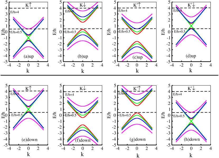
In Fig. 3 we demonstrate the spin polarization of both the and valleys for FS with the magnetisation directions up ( defined by ) and down ( defined by ) via an energy band diagram. The diagram clearly shows that different spin orientations behave differently in the and valleys at different values of the exchange field . To visualize this picture, we fix and show the dispersion for , , and for four different values of the tunable parameter , for the cases and . Note that we use , to denote the spins of the incoming (also reflected and transmitted) charge carriers and we use to denote the orientation of magnetic exchange. For the or case, at both and have a vanishing band gap. On the other hand, for , , and , the valleys at , , , are all gapped. Also note that due to the exchange splitting , the valley is shifted upwards for the spin while the valley is shifted downwards for the spin. The case for or is the other way around. Hence, it is clear that unlike in graphene, the contributions to the conductances from various spin configurations will not be identical for the and valleys.
III The scattering matrix
We model our FNF setup within the scattering matrix formalism Datta (1995) where we match the wave functions at each ferromagnetnormal interface to obtain the scattering matrix and find the conductances and the TMR . The wave functions for the valley in each of the three regions, , and can be written as
| (4) | |||||
| (7) |
where for , for and for . Note that we keep track of the sign of the charge carriers by including the index in all the regions (the sign of the charge carriers changes from electron-type to hole-type when is negative in any region). This actually happens for the anti-parallel configuration when energy of the incident charge carrier is below the induced magnetic field energy i.e. (). This charge reversal actually qualitatively changes the conductances, as was shown in graphene Zou et al. (2009).
We obtain the scattering matrix both for and by matching the wave functions (see Eq.(7)) at and and solving Eq.(16) numerically.
| (16) |
Further,
| (17) |
with , , , and . Since momentum is conserved in the direction and does not change, it is convenient to write the -component of the wave-vectors as
| (18) |
where is the conserved momentum in the direction.
IV Numerical results
In this section we present our numerical results for the FNF junction for different parameter regimes.
We first study the model described in Eq.(1) which has a spin-independent barrier in the normal silicene region. We compute the conductance using the transmission coefficients obtained in Eq.(16) for both the parallel () and the anti-parallel () configurations of spins, using the LandauerButtiker formalism Datta (1995). We use the scattering matrix to compute the total transmission probability for parallel and anti-parallel configurations by choosing the spins appropriately and for a particular incident angle (which fixes the angles in the other regions as well). The factor of in the transmission function is needed because the probablity flux density includes a factor of the velocity which is essentially . Since experimentally, it is not easy to control the angle of incidence of the impinging electron, we then compute the conductance by integrating over the possible angles of incidence and multiplying by the number of modes within the width of the silicene sample. At zero temperature, this leads us to a conductance given by
| (20) |
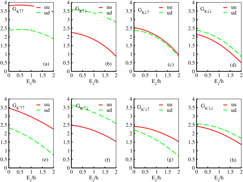
Here, is the critical angle of the incident particles which is needed to ensure propagating particles in the first and third regions and is given by for and for . Note that unlike the case for graphene, in silicene, the contributions at the two valleys are not identical and hence, we do not get the degeneracy factor of two. Instead, the contributions at both the valleys have to be computed independently and added to obtain the total conductance through the junction. Thus we define the total charge conductances , valley and the spin polarizations () and TMR through the FNF junction in terms of the following constituent conductances . Here, denotes (P) or (AP) spin configurations, denotes the valley ( or ) and denotes the spin of the incoming charge carrier in region 1 and denotes the spin of the outgoing charge carrier in region 3, which can be different, because we have spin-orbit coupling in the system. These conductances have been shown in Fig. 4 for both and . It is now easy to realize, in reference to the band diagrams given in Fig. 3 that the conductances go to zero when there is a gap in the density of states either in region 1 or 3. The maxima can also be understood by noting that the density of states at those values of are maximum and reduce both when is reduced or increased. This can be checked for each of the various conductances on a case by case basis.
The total charge conductance and the valley and spin polarizations for both the P () and AP () configurations are now defined as
| (21) |
Note that the indices in Eq.(21) gives rise to four possible spin configurations , , , for a FNF junction, of which and imply P configurations with and and denote AP configurations with .
Now from the knowledge of all the possible conductances, one can define the tunneling magnetoresistance (TMR) through the FNF geometry as
| (22) |
Note that the standard definition of TMR has in the denominator. However it is also sometimes defined with Moodera and Mathon (1999) and we choose this definition because in our case, vanishes at . This implies a singularity in the TMR which is avoided in our definition. Note that for , the difference in TMR between the two definitions is negligible. For , there are numerical differences, but no qualitative difference in the behavior of TMR with the two definitions.
The results are different for the energy regimes and , because of the difference in band structure, which has band gaps and hence no propagating states available for transport (see Fig. 3), for certain ranges of for . Since the main difference of silicene from graphene is the fact that the gap in silicene is tunable by the external electric field , we choose to focus on the dependence of conductances on . In cases, where we study the conductances as functions of other parameters such as the barrier strength or the exchange splitting , we present our results for three different values of .
Note that when , silicene is actually coplanar, i.e. the two sublattices are in same plane like in graphene. But the spin-orbit coupling in silicene is much stronger than in graphene Liu et al. (2011a). This increases or decreases the momentum of the incident charge carrier (see Eq.(17)) depending on the spin-polarization of the ferromagnetic silicene. Hence, we do not expect to reproduce the results of FNF junctions in graphene in the gapless regime.
IV.1 Spin-independent Barrier
Here we discuss the case where we have a finite spin-independent (scalar) barrier in the normal silicene region. The energy of the incident electron can be in the regime or and we present the behavior of the conductances and the TMR below. To carry out our numerical analyses, we have chosen to normalise all our energy scales by the Zeeman energy , so that all our results are in terms of dimensionless quantities. We also choose to measure conductances in units of .
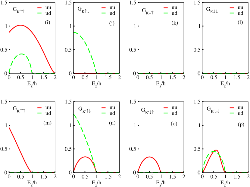
We first present the results for the various constituent conductances for the P and AP configuration in Fig. 4 in order to understand the behaviour of the conductances, the valley and spin polarizations and the TMR in various parameter regimes. The conductances are shown independently at the and the valleys as well as independently for the incoming () and the outgoing () spins of the charge carriers. In Figs. 4(a-h), we show the behaviour of the conductances at the and valleys, with respect to the dimensionless parameter for the four possibilities () in the regime for both the and configurations. Here the configuration corresponds to the majority spin density of states in the left and right FS regions being up spin (parallel to each other) and the configuration corresponds to the majority spin being opposite (anti-parallel) in the two regions. When charge carrier comes in from the left then it can either go to state or state in right region. So etc, denote spins of the incoming and scattered charge carriers. The behaviour of the various conductances in Figs. 4(a-h) can now be understood easily when analysed in terms of the band structure presented in Fig. 3.
For , the results have been presented for . Using the band diagram, it is easy to check that both at and , there are always electron states available for conductance for both the P and AP configurations and for all possible incoming and outgoing spins. The differences in the magnitude both at and valleys stems from the decrease in the momentum of the propagating states at the Fermi energy, as can be seen from the band diagram.
The results for is shown in Figs. 4(i-p) for . Consider the case for the valleys and . For , (red lines shown in Fig. 4(i) and Fig. 4(m)), the band diagram (see Fig. 3) shows that if we start with a spin up electron at the valley, (Fig. 4(i)) then there is a non-zero density of states for electrons in the third region for all values of until it reaches the value of 2 (the magenta line goes above the value of ). On the other hand, for the valley, (shown in Fig. 4(m)), there is no density of states for the electrons beyond (the blue line goes above the value ) in the third region. This explains why beyond for the valley and beyond for the valley, the conductances and are zero. It is also clear from the band diagram that for , its value increases from the value at , because the momenta of the electrons at grows (comparing the red and green lines) and beyond that it decreases (comparing the green, blue and magenta lines). On the other hand, for , it is clear that the momentum of the electrons at decreases as a function of (comparing the red, green and blue lines). This explains why the conductance rises initially and then falls beyond for and why it falls monotonically for .
A similar detailed analysis can also be made for the case as well as each of the other graphs in Figs. 4(j,k,l) and Figs. 4(n,o,p), which explains each feature of the graph. However, since the method is similar to what has been described above, we will not go through each one of the graphs in detail. The behaviour of the charge conductance, the valley and spin polarizations and the TMR are also now understandable, since we can explain how each of the constituents behave as a function of from the band diagram.
(a)
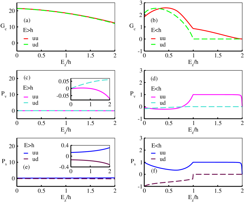
In Figs. 5(a), 5(c) and 5(e), we show the behaviour of the charge conductance () and the valley and spin polarizations ( and ) with respect to the dimensionless parameter for the P and AP configurations ( and ) in the regime. Note that in Fig. 5(a), and are both finite at and start decreasing as we increase the value of . is obtained by summing and , which in turn are obtained as
| (23) | |||||
and similarly for . In other words, the total charge conductance is obtained by summing over all the conductances in the panels (a) to (h) in Fig. 4.
In Fig. 5(c), and are plotted which are close to zero on the scale of the charge conductance. However, they are not identical, as shown in the inset. But it appears that in this regime, silicene has negligible valley polarization, similar to graphene, which in fact has no valley polarization at all, since the two valleys are identical. This can be understood because the valley polarization is simply proportional to , and as can be seen from Fig.4 that the magnitudes of the conductances at and are almost the same for . In Fig. 5(e), the behaviour of the spin polarization has been shown for both P () and AP () configurations, which is also very small in this regime. As shown in the inset, the spin polarization is positive for the P and negative for the AP configurations and increases as a function of . This difference is due to the spin-orbit coupling in silicene, whereas in graphene, they are much smaller, since the spin-orbit coupling is vanishingly small. Finally, in Fig. 6(a), the behavior of the TMR is shown as a function of by the green solid line in the regime. In this regime, the TMR is close to zero.
(b)
The right panels in Fig. 5 shows the behaviour of the charge conductance and the valley and spin polarizations , with respect to the dimensionless parameter , in the regime, for the same spin and polarization configurations mentioned earlier. These are just the appropriate sums and differences of the constituent conductances in Figs. 4(i-p). Here also, their behaviour is easy to understand by comparing each of the graphs in Figs. 4(i-p) with the band diagrams in Fig. 3 and noting when there is no density of states for the configuration in either the incoming or the outgoing spin configuration of the charge carriers. For instance, for the case, there is only one contribution for in Fig. 4(i) and for the case, there is no contribution for . This is because we have chosen and the blue line () in the band diagram goes above that line either for the incoming or scattered region for all cases in the configuration and all but one case in the configuration. In other words, their behaviour follows what is expected from the availabality or non-availability of propagating states at the and valleys as explained above in the discussion of Fig. 4.
The most interesting point to note is that the valley polarization and the spin polarization for the parallel or configuration is unity for in regime. This is simply because of the entire contribution to the conductance in this regime originates from . So the conductance is both fully valley and spin polarised and would be an important regime to achieve by tuning the incident electron energy and the electric field . In the anti-parallel or regime, the spin polarization can be tuned to negative values when , but without any valley polarization.
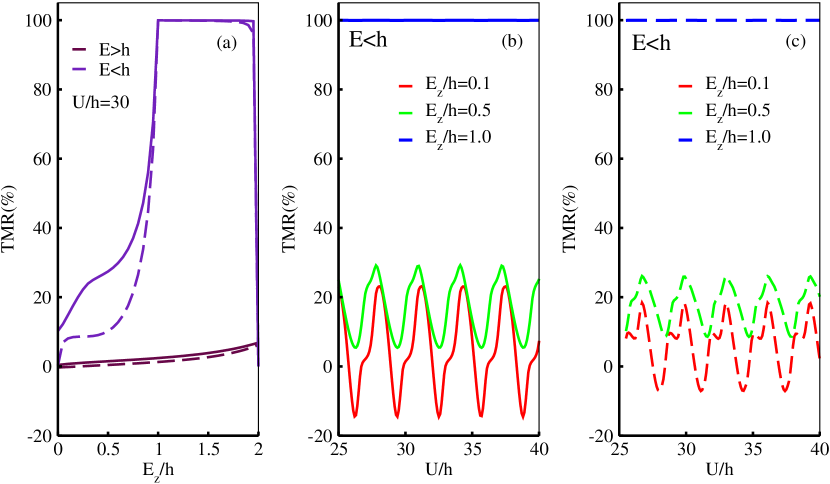
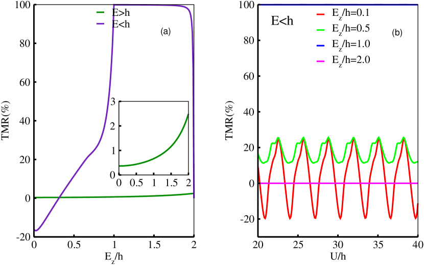
The behaviour of TMR is demonstrated in Figs. 6(a) and 6(b) for the regime. For , the TMR is negative and reaches its maximum negative value. Then the TMR increases as we increase the value of and changes sign and reaches saturation at since the conductance becomes fully spin polarised at that point. Note that we need to restrict the value of below two as the TMR takes an indeterminate form at due to the vanishing of both and (see Fig.5(c) and Eq.(22)) for all spin configurations. This is a consequence of our choice of the incident energy at .
The striking feature of positive to negative transition in the TMR also arises as we vary the strength of the potential barrier in the middle normal silicene region for different values of . This feature is shown in Fig. 6(b) where the TMR oscillates between positive and negative values with respect to for . Such oscillations of the TMR from positive to negative values have been reported earlier in Ref. Zou et al., 2009 in graphene, due to the change in the type of the charge carrier in the third region. Note also there is no significant qualitative change in the behavior of TMR even if we choose . This extra tunability of the TMR with respect to an external electric field is a unique feature of silicene that we wish to emphasize here in this manuscript.
IV.2 Spin dependent Barrier
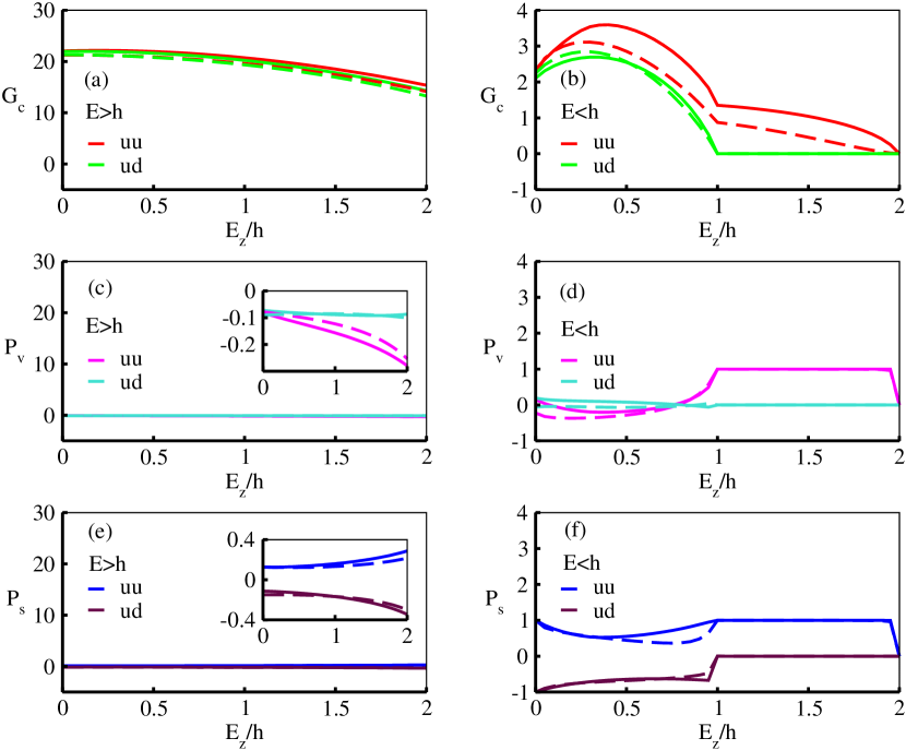
Here we discuss the effect of a spin-dependent barrier on the total charge conductance, valley and spin polarizations and the TMR. The barrier is modelled in the normal silicene region as which is shown in Fig. 2. Here positive (negative) represents the exchange splitting in the silicene barrier with its magnetization parallel (anti parallel) to the spin orientation of the FS in the first region.
In Figs. 7(a-f) we show the behaviour of the total charge conductances , spin and valley polarizations and , in the and regimes, for . Since the qualitative behavior of all the conductances remain similar to the spin independent barrier case, we do not show the behaviour of the conductances at the and valleys independently, or analyse the graphs in detail via the band structure. Similarly, in Figs 8(a-c), we show the behaviour of the TMR as a function of and as a function of as well (for ), for both . We find that the results are fairly similar to the spin-independent barrier case.
V Summary and conclusions
To summarize, in this paper, we have investigated the transport properties (charge conductance as well as spin and valley polarizations) and the TMR through a FNF junction in silicene. Here we have adopted the Landauer-Buttiker formalism to carry out our analysis. We show that the conductances and the TMR in this geometry can be tuned by an external electric field for each case (, , , ) in the left and right ferromagnetic silicene regions, for both parallel ( or ) and anti-parallel ( or ) configurations. For specific values of the electric field, we analyse both the charge conductance and valley and spin polarizations in terms of the independent behaviour of the conductances at the two valleys and the band structure at specific incident energies. We find that we can tune a fully valley polarised and also a fully spin polarised current through our setup via the external electric field. We also find that the TMR can be tuned to 100 % in this geometry via the electric field. This is one of the main conclusions of our analysis. We also show that the TMR through our setup exhibits an oscillatory behavior as a function of the strength of the barrier (both spin independent and spin dependent) in the normal silicene region. The TMR also changes sign between positive and negative values and such a transition can be tuned by the external electric field. This is another conclusion of our analysis. Hence, from the application point of view, our FNF geometry may be a possible candidate for making future generation spintronic devices out of silicene.
As far as the practical realization of such a FNF structure in silicene is concerned, it should be possible to fabricate such a geometry with the currently available experimental techniques. Ferromagnetic exchange in silicene may be achieved via proximity effect using a magnetic insulator, for instance, EuO Yang et al. (2013); Haugen et al. (2008). The typical spin orbit energy in silicene is Liu et al. (2011a). For an incident electron with energy and exchange energy , the maximum value of the spin and valley polarization as well as sign change of TMR from positive to negative value occur at an electric field , potential barrier of height , exchange splitting in the normal silicene region and width of the barrier .
Acknowledgments
One of us (A.S.) would also like to acknowledge the warm hospitality at the University of Basel, Switzerland, where this work was initiated.
References
- Ezawa (2015) M. Ezawa, “Monolayer topological insulators: Silicene, germanene and stanene,” (2015), arXiv:1503.08914 [cond-mat.mes-hall].
- Lalmi et al. (2010) B. Lalmi, H. Oughaddou, H. Enriquez, A. Kara, S. Vizzini, B. Ealet, and B. Aufray, Appl. Phys. Lett. 97, 223109 (2010).
- Padova et al (2010) P. D. Padova et al, Appl. Phys. Lett. 96, 261905 (2010).
- Vogt et al. (2012) P. Vogt, P. D. Padova, C. Quaresima, J. Avila, E. Frantzeskakis, M. C. Asensio, A. Resta, B. Ealet, and G. L. Lay, Phys. Rev. Lett. 108, 155501 (2012).
- Liu et al. (2011a) C. C. Liu, H. Jiang, and Y. Yao, Phys. Rev. B. 84, 195430 (2011a).
- Ezawa (2013a) M. Ezawa, Phys. Rev. B. 87, 155415 (2013a).
- Ezawa (2013b) M. Ezawa, New J. Phys. 14, 033003 (2013b).
- Drummond et al. (2012) N. D. Drummond, V. Zólyomi, and V. I. Falko, Phys. Rev. B. 85, 075423 (2012).
- Tao et al. (2014) L. Tao, E. Cinquanta, D. Chiappe, C. Grazianetti, M. Fanciulli, M. Dubey, A. Molle, and D. Akinwande, Nat. Nanotech. 10, 227 (2014).
- Guzmán-Verri and Lew Yan Voon (2007) G. G. Guzmán-Verri and L. C. Lew Yan Voon, Phys. Rev. B. 76, 075131 (2007).
- Ezawa (2012) M. Ezawa, Eur. Phys. J. B 85, 363 (2012).
- Liu et al. (2011b) C. C. Liu, W. Feng, and Y. Yao, Phys. Rev. Lett. 107, 076802 (2011b).
- Ezawa and Nagaosa (2013) M. Ezawa and N. Nagaosa, Phys. Rev. B. 88, 121401(R) (2013).
- Zutić et al. (2004) I. Zutić, J. Fabian, and S. Das Sarma, Rev. Mod. Phys. 76, 323 (2004).
- Wang et al (2015) Y. Wang et al, “Silicene spintronics,” (2015), arXiv:1506.00917 [cond-mat.mes-hall].
- Rachel and Ezawa (2014) S. Rachel and M. Ezawa, Phys. Rev. B 89, 195303 (2014).
- An et al. (2012) X. T. An, Y. Y. Zhang, J. J. Liu, and S. S. Li, New J. Phys. 14, 083039 (2012).
- Tsai et al. (2013) W. F. Tsai, C. Y. Huang, T. R. Chang, H. Lin, H. T. Jeng, and A. Bansil, Nat. Commn. 4, 1500 (2013).
- Shakouri et al. (2015) K. Shakouri, H. Simchi, M. Esmaeilzadeh, H. Mazidabadi, and F. M. Peeters, Phys. Rev. B 92, 035413 (2015).
- Datta (1995) S. Datta, Electronic transport in mesoscopic systems (Cambridge University Press, Cambridge, 1995).
- Zou et al. (2009) J. Zou, G. Jin, and Y. Ma, J. Phys. Cond. Matt. 21, 126001 (2009).
- Yokoyama (2013) T. Yokoyama, Phys. Rev. B. 87, 241409(R) (2013).
- Duppen et al. (2014) B. V. Duppen, P. Vasilopoulos, and F. M. Peeters, Phys. Rev. B 90, 035142 (2014).
- Yang et al. (2013) H. X. Yang, A. Hallal, D. Terrade, X. Waintal, S. Roche, and M. Chshiev, Phys. Rev. Lett. 110, 046603 (2013).
- Moodera and Mathon (1999) J. S. Moodera and G. Mathon, J. Magn. Magn. Mater. 200, 248 (1999).
- Haugen et al. (2008) H. Haugen, D. Huertas-Hernando, and A. Brataas, Phys. Rev. B 77, 115406 (2008).