High-Responsivity Graphene-Boron Nitride Photodetector and Autocorrelator in a Silicon Photonic Integrated Circuit
Abstract
Graphene and other two-dimensional (2D) materials have emerged as promising materials for broadband and ultrafast photodetection and optical modulation. These optoelectronic capabilities can augment complementary metal-oxide-semiconductor (CMOS) devices for high-speed and low-power optical interconnects. Here, we demonstrate an on-chip ultrafast photodetector based on a two-dimensional heterostructure consisting of high-quality graphene encapsulated in hexagonal boron nitride. Coupled to the optical mode of a silicon waveguide, this 2D heterostructure-based photodetector exhibits a maximum responsivity of 0.36 A/W and high-speed operation with a 3 dB cut-off at 42 GHz. From photocurrent measurements as a function of the top-gate and source-drain voltages, we conclude that the photoresponse is consistent with hot electron mediated effects. At moderate peak powers above 50 mW, we observe a saturating photocurrent consistent with the mechanisms of electron-phonon supercollision cooling. This nonlinear photoresponse enables optical on-chip autocorrelation measurements with picosecond-scale timing resolution and exceptionally low peak powers.
The past decades have seen concerted efforts to combine optical and electrical components into integrated optoelectronic circuits for a variety of applications, including optical interconnects Hochberg and Baehr-Jones (2010); Miller (2009); Bergman et al. (2014), biochemical sensing Estevez, Alvarez, and Lechuga (2012), and all-optical signal processingWabnitz and Eggleton (2015). The leading photodetector architectures, which form an essential technology for such circuits, are presently based on bulk semiconductor materials, predominantly Ge Wang and Lee (2011) and InPLiang et al. (2010). However, the integration of bulk semiconductor-based on-chip detectors has faced important challenges, including in some cases front-end changes in complementary metal-oxide-semiconductor (CMOS) processing, a spectral response limited by the material’s bandgap—e.g. up to the L telecommunication band for strained Ge—and an intrinsic speed limited by the material’s carrier mobility. In addition, because of the weak nonlinear optical response of these bulk semiconductor materials, high optical powers are required in nonlinear applications including optical pulse characterization, sampling, and signal processingSlavík et al. (2010); Ferdous et al. (2011); Weiner (2000). Recently, the family of two-dimensional (2D) materials has emerged as an alternative optoelectronic platform with new functionalitiesKoppens et al. (2014); Avouris and Freitag (2014), including broadband ultrafast photodetectionXia et al. (2014); Gan et al. (2013a); Youngblood et al. (2015); Schall et al. (2014); Tielrooij et al. (2015), on-chip electro-optic modulationLiu et al. (2011); Gao et al. (2015); Phare et al. (2014); Hu and Pantouvaki (2014), light emissionBaugher et al. (2014); Pospischil, Furchi, and Mueller (2014), saturable absorptionSun et al. (2010), and parametric nonlinearitiesGu et al. (2012); Hendry et al. (2010); Gullans et al. (2013). Moreover, distinct 2D materials can be assembled nearly defect-free into entirely new types of 2D heterostructuresWang et al. (2013a); Geim and Grigorieva (2013), enabling optoelectronic properties and device concepts that were not feasible using bulk semiconductors.
Here, we introduce a 2D heterostructure consisting of single-layer graphene (SLG) encapsulated by hexagonal boron nitride (hBN) that enables both high-responsivity photodetection and ultrafast pulse metrology in a compact waveguide-integrated design. The mobility of BN-encapsulated graphene can reach up to 80,000 cm2/Vs at room temperature, exceeding that of traditional semiconductors such as Ge by 1-3 orders of magnitude. We use one-dimensional contacts to the hBN/SLG/hBN stack combined with a wide channel design to achieve a device resistance as low as 77 . We measure operating speeds exceeding 40 GHz (3dB cut-off) and a record-high detection responsivity exceeding 350 mA/W, approaching responsivities of on-chip Si-Ge photodetectorsWang and Lee (2011). We fabricated this 2D heterostructure in a back-end-of-the-line (BEOL) step on a silicon-on-oxide (SOI) photonic integrated circuit (PIC), which was fabricated in a CMOS-compatible process. The strong electron-electron interaction and weak electron-phonon coupling of the SLGSong et al. (2011); Song, Reizer, and Levitov (2012); Graham et al. (2012) result in a nonlinear photoresponse above mW of peak input power, enabling direct autocorrelation characterization of ultrafast pulses. Unlike traditional free-space autocorrelators, optical nonlinear time-lens techniquesFoster et al. (2008), and frequency-resolved optical gating (FROG)Tien et al. (2009); Walmsley and Dorrer (2009), this on-chip 2D heterostructure-based autocorrelator does not require parametric nonlinear effects, passive dispersive optics, or separate photodetectors. We measured a minimum timing resolution of 3 ps with a minimum required peak power of 67 mW, comparable to the the autocorrelators based on two photon absorption (TPA) of silicon or III-V compound semiconductors. The ability for high responsivity photodetection and ultrafast optical autocorrelation in one small-footprint device opens the door to new applications and device concepts in integrated optics.
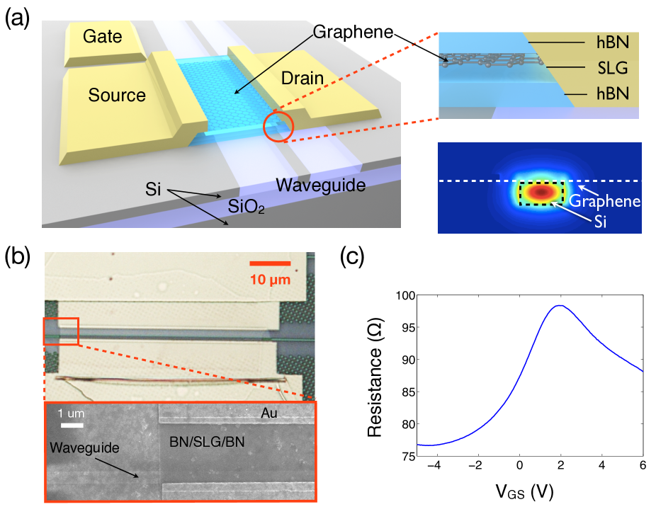
Fig. 1a illustrates the device architecture. Silicon waveguides were fabricated in an SOI wafer with a 220 nm silicon membrane on a 3-m-thick SiO2 layer. This step used shallow trench isolation (STI) commonly used in CMOS processing. A waveguide width of 520 nm supports a single transverse-electric (TE) mode shown in the simulated mode in Fig. 1a (lower right panel). The chip was planarized by backfilling with a thick SiO2 layer, followed by chemical mechanical polishing to reach the top silicon surface. We then transferred the multilayered hBN/SLG/hBN stack onto the photonic chip using van der Waals (vdW) assembly Wang et al. (2013a). The graphene channel spans 40 m of the waveguide. We applied one-dimensional edge contacts to the encapsulated graphene layer using a series of etching and metallization stepsWang et al. (2013a). A polymer electrolyte (poly(ethylene oxide) and LiClO4) layer was spin-coated on the entire chip to gate the graphene deviceLu et al. (2004).
Fig. 1b shows the completed structure. The drain electrode is positioned only 200 nm from the waveguide to induce a pn junction near the optical modePospischil et al. (2013). Confocal scanning beam excitation measurements confirm a strong photoresponse region near this metal/graphene interface, as demonstrated previously Gan et al. (2013b) and shown for this particular device in Fig. S1 in the supporting information. Measurements of the device resistance as a function of gate voltage, shown in Fig. 1c, indicate a charge neutrality point (CNP) at a gate-source voltage of = 2 V and a minimum device resistance of 77 . From similar hBN/SLG/hBN stacks assembled on SiO2 substrates, which also included a Hall-bar geometry that was not possible for us to include on the waveguide-integrated device, the mobility of graphene is in the range of 40,000–60,000 cm2/Vs at carrier densities between 2–4 cm-2Wang et al. (2013a).
We characterized the transmission of the completed device in the telecommunications band at 1550 nm, using lensed fibers for edge-coupling to SiN mode converters at the input and output of the -mm-long Si waveguide, as reported previously Gan et al. (2013b). The hBN/SLG/hBN detector stack is located at the center of the waveguide, 2 mm from either edge facet. Depositing the stack increased the waveguide transmission loss from 11 dB to 13.2 dB. Attributing this 2.2 dB excess loss to the 40-m-long graphene-waveguide overlap, we calculate an absorption coefficient of 0.055 dB/m. This coefficient is slightly higher than the absorption of 0.043 dB/m that we estimated independently from a finite element simulation of the waveguide evanescent field coupling to the SLGGan et al. (2013b) (note that the hBN is transparent in the telecom band since it has a bandgap of 5.2 eV). We attribute the slightly higher loss (0.48 dB) of the experimental device to additional scattering and reflection losses at the waveguide-detector stack interface. We observed negligible transmission loss from the electrolyte.
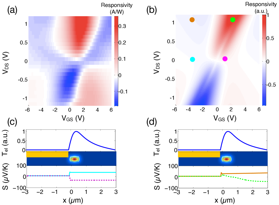
Fig. 2a presents responsivity measurements as a function of and when the detector is illuminated via the waveguide at 25 W continuous-wave (c.w.) laser inside the waveguide. Here the responsivity is defined as the ratio of the short-circuit photocurrent (supporting information) to the optical power in the waveguide, . Unlike previous waveguide-integrated graphene photodetectors, which included only drain-source voltage control Gan et al. (2013b); Pospischil et al. (2013); Wang et al. (2013b), the additional top electrolyte-gate allows us to independently tune the graphene Fermi level and electric field across the waveguide mode. Scanning and produces a six-fold pattern in the photocurrent, which qualitatively matches the behavior of the photothermoelectric (PTE) effectSong et al. (2011); Gabor et al. (2011). The photocurrent reaches a maximum of 0.36 A/W at VGS = 2 V and VDS = 1.2 V; this represent a more than three-fold improvement over previous waveguide-integrated graphene photodetectorsGan et al. (2013b); Pospischil et al. (2013); Wang et al. (2013b).
To explain the measured six-fold pattern in the responsivity map, we consider the PTE effect for the metal/graphene junction that overlaps with the waveguide. The evanescent field from the waveguide creates photo-excited carriers in the SLG, which rapidly thermalize, increasing the local electron temperature. Fig. 2c (top panel) shows the numerically solved local electron temperature across the source and drain contacts of the detector (supporting information). The photo-excited hot-electrons diffuse and create a potential gradient , where is the temperature gradient of the hot electrons and is the Seebeck coefficient. The total photocurrent collected between the source and drain contacts is given by
| (1) |
where is the conductance of graphene and the is length of the graphene channel. From the Mott formulaAshcroft and Mermin (1976); Liu et al. (2012); Lemme et al. (2011); Song et al. (2011), can be expressed as
| (2) |
where is the Boltzmann constant, is the lattice temperature, is the electron charge, is the conductivity of graphene, and is the chemical potential. Eq. 2 indicates that depends strongly on the carrier density and the chemical potential of graphene, which can be tuned by and in our device. Fig. 2c and 2d show examples of the spatially resolved S(x) using parameters obtained from the measured conductance and the capacitance of the electrolyte (supporting information). By integrating and along the source and drain contacts using Eq. 1, we can therefore calculate the photocurrent with respect to and , producing the photocurrent mapping in Fig. 2b, which shows a six-fold pattern qualitatively similar to the measured gate- and bias-dependent responsivity. It is also important to consider photovoltaic (PV) effects that generate photocurrent at the graphene junction. However, the PV effect only produces a single sign reversal with respect to VGS and VDS and does not agree to the measured six-fold pattern in the experimentSong et al. (2011); Lemme et al. (2011); Liu et al. (2012). We therefore estimate the PV effect to be small compared with the PTE, which is confirmed by theoretical approximations presented in the supporting information.
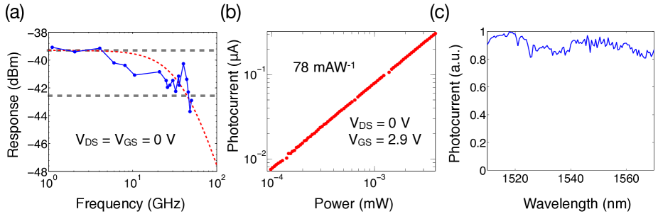
To test the dynamic response of the hBN/SLG/hBN detector, we coupled two narrowband (1 MHz) laser sources with a detuning frequency ranging from 1 to 50 GHz into the waveguide. The interference of these two laser fields produces an intensity in the detector that oscillates at frequency . Fig.3a displays the measured power at , obtained on an electrical spectrum analyzer (maximum frequency 50 GHz) via high-speed RF probes (Cascade FPC-GS-150). This measurement indicates a 3-dB cutoff frequency at 42 GHz, matching the highest reported graphene photodetector speeds Schall et al. (2014). We observed this ultrafast photoresponse even under zero drain-source bias, which distinguishes graphene from typical semiconductor high-speed photodiodesWang and Lee (2011). The detected photocurrent at = 0 (Fig. 3b) linearly reduces with input power, indicating vanishing dark current. The responsivity at zero bias reaches 78 mA/W. Accounting for the fact that the graphene absorbs only dB of optical power in the waveguide, we can thus estimate an internal quantum efficiency of 16-19%. As shown in Fig. 3c, the spectral response of the detector under c.w. laser excitation varies uniformly in the spectral range from 1510 nm to 1570 nm.
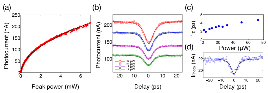
We next tested the detector using 250-fs pulses at 1800 nm, produced by an optical parametric oscillator pumped by a Ti:Sapphire oscillator with 78 MHz repetition rate. As shown in Fig. 4a, the photocurrent shows a nonlinear photoresponse that is fit well by . This approximately square root dependence in photocurrent with pump power suggests a supercollision-dominated cooling mechanism, for which Graham et al. (2012). Using this nonlinear photoresponse, we characterized our photodetector’s ultimate speed limitations, which are dictated by the internal carrier dynamics. Fig. 4b plots photocurrent traces as a function of the time delay between pairs of 250-fs laser pulses for a range of incident powers. These traces show a clear dip at with a width that corresponds to the carrier relaxation time, i.e., the time needed for the graphene detector to return to equilibrium. The half-width at half-maximum response times are plotted in Fig. 4c for a sweep of input powers. The minimum response time is approximately 3 ps. The slight increase of the response time at higher input power is unclear to us at this point and requires future studies.
The picosecond-scale nonlinear photocurrent from the photodetector can be used for on-chip autocorrelation measurements for, e.g., ultrafast optical sampling. We tested the autocorrelator with an average power of only 1.4 W (peak power of 67 mW). The autocorrelation trace (Fig. 4d) shows a clear dip with a minimum resolution down to 3ps. The required peak power is less than free space autocorrelators based on parametric frequency conversion 111Reef femtosecond autocorrelator Reef-RTD and Femtochrome Research Inc. FR-103WS, and is also comparable to TPA-based semiconductor autocorrelators with waveguide or cavity integrationHayat et al. (2011); Duchesne et al. (2010); Liang et al. (2002). We noticed that the femtosecond-scale heating of the hot-electrons in graphene in a recent report could in principle improve the timing resolution of the on-chip autocorrelator to sub-50 fsTielrooij et al. (2015). It is also important to note that this graphene-based autocorrelator supports a broad spectral range that is identical to the spectral response of the graphene detector, which, in this work, is from 1500 nm to 1800 nm.
In summary, we have demonstrated a compact, high-speed and high-responsivity graphene photodetector integrated into a CMOS-compatible PIC. The maximum responsivity of the detector is 0.36 A/W with a high-speed 42 GHz cut-off frequency. The measured photocurrent of the detector as a function of and can be modeled by the PTE effect at the junction near the metal/graphene interface. Under pulsed excitation, the nonlinear photocurrent response enables the characterization of ultrafast optical pulses and presents a new functionality of such a photodetector for autocorrelation and ultrafast optical sampling measurements. The peak power required for the autocorrelator is as low as 67 mW with a timing resolution of 3 ps. Our work shows the potential of 2D heterostructure-based photodetector architectures integrated in CMOS-compatible fashion with silicon PICs. Moreover, the unique nonlinear photoresponse of graphene enables a versatile platform for ultrafast metrology, which may also find applications for on-chip mode-locked pulse generation and pulse shaping on a single chip. The integrated photodetector and autocorrelator promise a broad range of applications ranging from optical communications to signal processing and ultrafast optics.
Acknowledgements.
The authors thank Prof. Xuetao Gan for helpful discussion on the experiment scheme and data analysis. Financial support was provided by the Office of Naval Research (Awards N00014-13-1-0662 and N00014-14-1-0349). Device fabrication was partly carried out at the Center for Functional Nanomaterials, Brookhaven National Laboratory, which is supported by the US Department of Energy, Office of Basic Energy Sciences (contract no. DE-AC02- 98CH10886). R.-J.S. was supported in part by the Center for Excitonics, an Energy Frontier Research Center funded by the US Department of Energy, Office of Science, Office of Basic Energy Sciences under award no. DE-SC0001088. YF. W. was supported in part by Tsinghua Xuetang Talents Program.References
- Hochberg and Baehr-Jones (2010) M. Hochberg and T. Baehr-Jones, “Towards fabless silicon photonics,” Nature Photonics 4, 492–494 (2010).
- Miller (2009) D. A. B. Miller, “Device Requirements for Optical Interconnects to Silicon Chips,” Proceedings of the IEEE 97, 1166–1185 (2009).
- Bergman et al. (2014) K. Bergman, L. P. Carloni, A. Biberman, J. Chan, and G. Hendry, Photonic Network-on-Chip Design (Springer, 2014).
- Estevez, Alvarez, and Lechuga (2012) M. Estevez, M. Alvarez, and L. Lechuga, “Integrated optical devices for lab-on-a-chip biosensing applications,” Laser & Photonics Reviews 6, 463–487 (2012).
- Wabnitz and Eggleton (2015) S. Wabnitz and B. J. Eggleton, All-Optical Signal Processing: Data Communication and Storage Applications, Vol. 194 (Springer, 2015).
- Wang and Lee (2011) J. Wang and S. Lee, “Ge-photodetectors for Si-based optoelectronic integration.” Sensors (Basel, Switzerland) 11, 696–718 (2011).
- Liang et al. (2010) D. Liang, G. Roelkens, R. Baets, and J. E. Bowers, “Hybrid Integrated Platforms for Silicon Photonics,” Materials 3, 1782–1802 (2010).
- Slavík et al. (2010) R. Slavík, F. Parmigiani, J. Kakande, C. Lundström, M. Sjödin, P. A. Andrekson, R. Weerasuriya, S. Sygletos, A. D. Ellis, L. Grüner-Nielsen, D. Jakobsen, S. r. Herstrø m, R. Phelan, J. O’Gorman, A. Bogris, D. Syvridis, S. Dasgupta, P. Petropoulos, and D. J. Richardson, “All-optical phase and amplitude regenerator for next-generation telecommunications systems,” Nature Photonics 4, 690–695 (2010).
- Ferdous et al. (2011) F. Ferdous, H. Miao, D. Leaird, and K. Srinivasan, “Spectral line-by-line pulse shaping of on-chip microresonator frequency combs,” Nature … 5, 770–776 (2011).
- Weiner (2000) A. M. Weiner, “Femtosecond pulse shaping using spatial light modulators,” Review of Scientific Instruments 71, 1929 (2000).
- Koppens et al. (2014) F. H. L. Koppens, T. Mueller, P. Avouris, a. C. Ferrari, M. S. Vitiello, and M. Polini, “Photodetectors based on graphene, other two-dimensional materials and hybrid systems,” Nature Nanotechnology 9, 780–793 (2014).
- Avouris and Freitag (2014) P. Avouris and M. Freitag, “Graphene Photonics, Plasmonics, and Optoelectronics,” IEEE Journal of Selected Topics in Quantum Electronics 20, 6000112–6000112 (2014).
- Xia et al. (2014) F. Xia, H. Wang, D. Xiao, M. Dubey, and A. Ramasubramaniam, “Two-dimensional material nanophotonics,” Nature Photonics 8, 899–907 (2014).
- Gan et al. (2013a) X. Gan, R.-J. Shiue, Y. Gao, S. Assefa, J. Hone, and D. Englund, “Controlled light-matter interaction in graphene electrooptic devices using nanophotonic cavities and waveguides,” Selected Topics in Quantum Electronics, IEEE Journal of 20, 6000311–6000311 (2013a).
- Youngblood et al. (2015) N. Youngblood, C. Chen, S. J. Koester, and M. Li, “Waveguide-integrated black phosphorus photodetector with high responsivity and low dark current,” Nature Photonics 9 (2015), 10.1038/nphoton.2015.23.
- Schall et al. (2014) D. Schall, D. Neumaier, M. Mohsin, B. Chmielak, J. Bolten, C. Porschatis, A. Prinzen, C. Matheisen, W. Kuebart, B. Junginger, W. Templ, A. L. Giesecke, and H. Kurz, “50 gbit/s photodetectors based on wafer-scale graphene for integrated silicon photonic communication systems,” ACS Photonics 1, 781–784 (2014), http://dx.doi.org/10.1021/ph5001605 .
- Tielrooij et al. (2015) K. J. Tielrooij, L. Piatkowski, M. Massicotte, a. Woessner, Q. Ma, Y. Lee, K. S. Myhro, C. N. Lau, P. Jarillo-Herrero, N. F. van Hulst, and F. H. L. Koppens, “Generation of photovoltage in graphene on a femtosecond timescale through efficient carrier heating,” Nature Nanotechnology 10, 437–443 (2015).
- Liu et al. (2011) M. Liu, X. Yin, E. Ulin-Avila, B. Geng, T. Zentgraf, L. Ju, F. Wang, and X. Zhang, “A graphene-based broadband optical modulator.” Nature 474, 64–67 (2011).
- Gao et al. (2015) Y. Gao, R.-J. Shiue, X. Gan, L. Li, C. Peng, I. Meric, L. Wang, A. Szep, D. Walker, J. Hone, and D. Englund, “High-speed electro-optic modulator integrated with graphene-boron nitride heterostructure and photonic crystal nanocavity,” Nano Letters 15, 2001–2005 (2015), pMID: 25700231, http://dx.doi.org/10.1021/nl504860z .
- Phare et al. (2014) C. T. Phare, Y.-H. D. Lee, J. Cardenas, and M. Lipson, “30 ghz zeno-based graphene electro-optic modulator,” arXiv preprint arXiv:1411.2053 (2014).
- Hu and Pantouvaki (2014) Y. Hu and M. Pantouvaki, “Broadband 10Gb/s Graphene Electro-Absorption Modulator on Silicon for Chip-Level Optical Interconnects,” …(IEDM), 2014 IEEE … , 128–131 (2014).
- Baugher et al. (2014) B. W. H. Baugher, H. O. H. Churchill, Y. Yang, and P. Jarillo-Herrero, “Optoelectronic devices based on electrically tunable p-n diodes in a monolayer dichalcogenide.” Nature nanotechnology 9, 262–7 (2014).
- Pospischil, Furchi, and Mueller (2014) A. Pospischil, M. M. Furchi, and T. Mueller, “Solar-energy conversion and light emission in an atomic monolayer p-n diode.” Nature nanotechnology 9, 257–61 (2014).
- Sun et al. (2010) Z. Sun, T. Hasan, F. Torrisi, D. Popa, G. Privitera, F. Wang, F. Bonaccorso, D. M. Basko, and A. C. Ferrari, “Graphene Mode-Locked Ultrafast Laser,” ACS Nano 4, 803–810 (2010).
- Gu et al. (2012) T. Gu, N. Petrone, J. F. Mcmillan, A. V. D. Zande, M. Yu, G. Q. Lo, D. L. Kwong, J. Hone, and C. W. Wong, “Regenerative oscillation and four-wave mixing in graphene optoelectronics,” Nature photonics 43, 1–6 (2012).
- Hendry et al. (2010) E. Hendry, P. J. Hale, J. Moger, A. K. Savchenko, and S. A. Mikhailov, “Coherent Nonlinear Optical Response of Graphene,” Physical Review Letters 105, 097401 (2010).
- Gullans et al. (2013) M. Gullans, D. Chang, F. Koppens, F. de Abajo, and M. Lukin, “Single-Photon Nonlinear Optics with Graphene Plasmons,” Physical Review Letters 111, 247401 (2013).
- Wang et al. (2013a) L. Wang, I. Meric, P. Y. Huang, Q. Gao, Y. Gao, H. Tran, T. Taniguchi, K. Watanabe, L. M. Campos, D. a. Muller, J. Guo, P. Kim, J. Hone, K. L. Shepard, and C. R. Dean, “One-dimensional electrical contact to a two-dimensional material.” Science (New York, N.Y.) 342, 614–7 (2013a).
- Geim and Grigorieva (2013) A. K. Geim and I. V. Grigorieva, “Van der Waals heterostructures.” Nature 499, 419–25 (2013).
- Song et al. (2011) J. C. W. Song, M. S. Rudner, C. M. Marcus, and L. S. Levitov, “Hot carrier transport and photocurrent response in graphene.” Nano letters 11, 4688–4692 (2011).
- Song, Reizer, and Levitov (2012) J. C. W. Song, M. Y. Reizer, and L. S. Levitov, “Disorder-Assisted Electron-Phonon Scattering and Cooling Pathways in Graphene,” Physical Review Letters 109, 106602 (2012).
- Graham et al. (2012) M. W. Graham, S.-F. Shi, D. C. Ralph, J. Park, and P. L. McEuen, “Photocurrent measurements of supercollision cooling in graphene,” Nature Physics 9, 103–108 (2012).
- Foster et al. (2008) M. a. Foster, R. Salem, D. F. Geraghty, A. C. Turner-Foster, M. Lipson, and A. L. Gaeta, “Silicon-chip-based ultrafast optical oscilloscope.” Nature 456, 81–4 (2008).
- Tien et al. (2009) E.-K. Tien, X.-Z. Sang, F. Qing, Q. Song, and O. Boyraz, “Ultrafast pulse characterization using cross phase modulation in silicon,” Applied Physics Letters 95, 051101 (2009).
- Walmsley and Dorrer (2009) I. A. Walmsley and C. Dorrer, “Characterization of ultrashort electromagnetic pulses,” Advances in Optics and Photonics 1, 308 (2009).
- Lu et al. (2004) C. Lu, Q. Fu, S. Huang, and J. Liu, “Polymer Electrolyte-Gated Carbon Nanotube Field-Effect Transistor,” Nano Letters 4, 623–627 (2004).
- Pospischil et al. (2013) A. Pospischil, M. Humer, M. M. Furchi, D. Bachmann, R. Guider, T. Fromherz, and T. Mueller, “CMOS-compatible graphene photodetector covering all optical communication bands,” Nature Photonics 7, 892–896 (2013).
- Gan et al. (2013b) X. Gan, R.-J. Shiue, Y. Gao, I. Meric, T. F. Heinz, K. Shepard, J. Hone, S. Assefa, and D. Englund, “Chip-integrated ultrafast graphene photodetector with high responsivity,” Nature Photonics 7, 883–887 (2013b).
- Wang et al. (2013b) X. Wang, Z. Cheng, K. Xu, H. K. Tsang, and J.-B. Xu, “High-responsivity graphene/silicon-heterostructure waveguide photodetectors,” Nature Photonics 7, 888–891 (2013b).
- Gabor et al. (2011) N. M. Gabor, J. C. W. Song, Q. Ma, N. L. Nair, T. Taychatanapat, K. Watanabe, T. Taniguchi, L. S. Levitov, and P. Jarillo-Herrero, “Hot carrier-assisted intrinsic photoresponse in graphene.” Science (New York, N.Y.) 334, 648–52 (2011).
- Ashcroft and Mermin (1976) N. W. Ashcroft and N. D. Mermin, Solid State Physics (Holt, Rinehart and Winston, 1976) p. 826.
- Liu et al. (2012) C.-H. Liu, N. M. Dissanayake, S. Lee, K. Lee, and Z. Zhong, “Evidence for extraction of photoexcited hot carriers from graphene.” ACS nano 6, 7172–6 (2012).
- Lemme et al. (2011) M. C. Lemme, F. H. L. Koppens, A. L. Falk, M. S. Rudner, H. Park, L. S. Levitov, and C. M. Marcus, “Gate-activated photoresponse in a graphene p-n junction.” Nano letters 11, 4134–4137 (2011).
- Note (1) Reef femtosecond autocorrelator Reef-RTD and Femtochrome Research Inc. FR-103WS.
- Hayat et al. (2011) A. Hayat, A. Nevet, P. Ginzburg, and M. Orenstein, “Applications of two-photon processes in semiconductor photonic devices: invited review,” Semiconductor Science and Technology 26, 083001 (2011).
- Duchesne et al. (2010) D. Duchesne, L. Razzari, L. Halloran, and M. Gigu, “Two-photon Autocorrelation in a MQW GaAs Laser at 1 . 55 µ m,” 0, 267–272 (2010).
- Liang et al. (2002) T. K. Liang, H. K. Tsang, I. E. Day, J. Drake, A. P. Knights, and M. Asghari, “Silicon waveguide two-photon absorption detector at 1.5 m wavelength for autocorrelation measurements,” Applied Physics Letters 81, 1323 (2002).