Electronic structure of tungsten-doped vanadium dioxide
Abstract
A common method of adjusting the metal-insulator transition temperature of M1 VO2 is via disruption of the Peierls pairing by doping, or inputting stress or strain. However, since adding even small amounts of dopants will change the band structure, it is unclear how doped VO2 retains its insulating character observed in experiments. While strong correlations may be responsible for maintaining a gap, theoretical evidence for this has been very difficult to obtain due to the complexity of the many-body problem involved. In this work we use GW calculations modified to include strong local k-space interactions to investigate the changes in band structure from tungsten doping. We find that the combination of carrier doping and the experimentally observed structural defects introduced by inclusion of tungsten are consistent with a change from band-like to Mott-insulating behavior.
pacs:
71.30.+h,71.27.+a,74.20.Pq,75.10.-b,71.20.-bIntroduction: Vanadium dioxide is considered a prototypical strongly correlated material, which undergoes a first order insulator metal transition at 340 K from a low temperature monoclinic structure to a high temperature, metallic tetragonal structure Goodenough (1971). In the last decade, advances in nanofabrication techniques have seen an explosion of interest in devices based on VO2 nanobeams Wei et al. (2012); Park et al. (2013), which show enormous potential for sensors Guo et al. (2011) and even new transistor gates Nakano et al. (2012). Dynamical Mean Field Theory Biermann et al. (2005) and GW calculations Gatti et al. (2007) suggest that pure VO2’s insulating character results from the three-dimensional pairings that occur in the transition from tetragonal to monoclinic which fill the valence band, with strong correlations in the metallic form responsible for driving the transition to the insulating state Biermann et al. (2005).
Many methods of controlling the critical temperature revolve around disrupting this pairing, such as the input of stress or strain Wei et al. (2009), or doping Lawton and Theby (1995). Doping with tungsten has long been known to reduce Tc by 23 K per atomic percent of tungsten Lawton and Theby (1995). However, when viewed through the lens of band theory, this presents something of a paradox, as doping carriers into pure VO2 should result in a metallic structure. Experiments confirm however, that VO2 doped with 10 % tungsten remains insulating Tang et al. (1985). In addition, photoemission experiments reveal that tungsten assumes the place of a vanadium atom in the VO2 lattice, but does not Peierls pair with neighbouring atoms Tang et al. (1985), despite having the valence electrons to do so. Rather, the local environment of the tungsten is tetragonal, while the structure retains an overall symmetry. This is in contrast to doping with chromium, which despite being in the same group as tungsten, promotes the formation of the Mott insulating M2 structure at dopant percentages as low as 0.5 % Marezio et al. (1971).
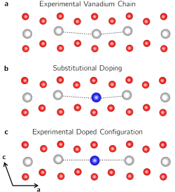
Figure 1 compares the different geometries involved: Figure 1a illustrates the Peierls paired and antiferroelectrically distorted vanadium chain in the undoped compound. Figure 1b illustrates a substitutionally doped chain, in which the tungsten adopts the position of a vanadium atom. Figure 1c corresponds to the experimentally observed Tang et al. (1985); Booth and Casey (2009) tungsten environment; the tungsten atom sits equidistant from the neighbouring vanadium atoms, and in the center of the oxygen octadehron, i.e. with no Peierls pairing or antiferroelectric distortion. Given that the insulating state occurs via the vanadium atoms in the tetragonal structure forming pairs and undergoing an antiferroelectric distortion Goodenough (1971), disruption of this structural rearrangement as per Figure 1c, combined with the extra carriers might appear from a purely band theoretical view to transform tungsten-doped VO2 to a metallic structure. Unless of course the experimentally observed insulating behavior in the doped structure arises due to strong correlations in the partially filled band.
a b c
The resolution of such a paradox from a computational perspective has to-date been out of reach, due to the failure of ab initio methods to reproduce Mott physics Burke (2012). Band theory in particular fails spectacularly Imada et al. (1998), such that even qualitative predictions are almost always inaccurate. For example, DFT characteristically predicts Mott insulators to be metallic Anisimov et al. (1991); Burke (2012), a significant issue when designing materials to take advantage of their insulating behavior. Recently however, it was revealed that GW calculations can be modified to include strong local k-space correlations (the “Partially Screened GW” method or PS-GW) Booth et al. (2016), and can reproduce two significant characteristics of Mott physics: the splitting of partially filled bands into the upper and lower Hubbard bands, and the giant transfer of spectral weight upon carrier doping. The ability of this approach to reproduce these characteristics means that it is now possible to investigate systems in which the rigid band model fails, and in this work we apply it to the study of tungsten-doped VO2.
Methods: The M1 VO2 structure Andersson (1954) was first relaxed to the ground state using PBE-GGA Perdew et al. (1996) Density Functional Theory (DFT) and the Brillouin zone integration method of Bloechl et al. Blochl et al. (1994). , , Monkhorst-Pack Monkhorst and Pack (1976) k-space grids were used for the 25 %, 12.5 % and 3.1 % tungsten-doped structures respectively. These consisted of one, two and eight VO2 unit cells in , , and configurations in which a single vanadium atom was replaced with tungsten. A discussion motivating the use of geometry relaxation to generate input structures in presented in the Supporting Information. The GW calculations were performed using the implementation of Shishkin and Kresse Shishkin and Kresse (2006, 2007) as contained in the Vienna Ab Initio Simulation Package (VASP) Kresse and Furthmüller (1996), after first calculating input wavefunctions using DFT with the PBEPerdew et al. (1996) functional. The standard, or unmodified, GW calculations were performed on a frequency grid of 30 points, using a cutoff energy of 200 eV. Strong correlations were included by setting the derivatives of the wavefunctions with respect to the k-point grid to zero (the PS-GW method, see Booth et al. Booth et al. (2016)). Five self-consistency steps were used for the 12.5 % doped structures, while four and two steps were used for the 12.5 % and 3.1 % doped structures respectively. All strongly correlated calculations were performed at a single frequency point, =0 Booth et al. (2016).
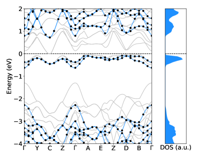
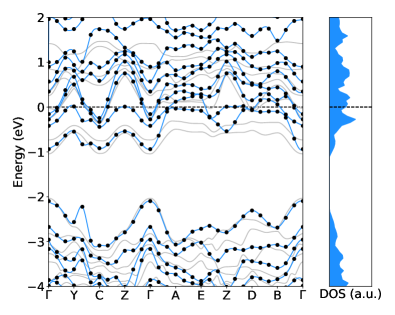
Discussion: Figure 2a illustrates the results of unmodified G0W0 calculations (i.e. not PS-GW) on the M1 structure of VO2 (corresponding to the vanadium chain environment of Figure 1a). In all plots presented in this work the Fermi level is set to zero energy. The GW band structure (black filled circles) exhibits substantial splitting of the valence and conduction bands at EF in contrast to the DFT bands (gray lines), in which the gap manifests as a slight splitting of the bands at EF. The calculated GW gap is 0.70 eV, in excellent agreement with photoemission measurements (also 0.70 eV Shin et al. (1990)). Therefore, for M1 VO2, screening the Hartree-Fock interaction with the dielectric matrix resulting from non-interacting Green functions is sufficient to reproduce the experimental characteristics of the undoped structure.
a b
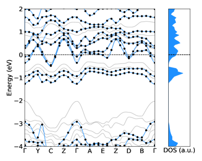
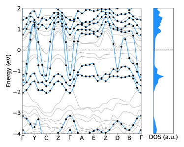
However, Figure 2b indicates that for substitutionally tungsten-doped VO2 this is not the case. This figure plots an unmodified GW calculation of a doped configuration identical to that of Figure 1b and it is clear that the Fermi level now intersects the conduction band minima at , , and . The curvatures of the DFT bands are in reasonable agreement with the splines fitted to the GW data which indicates that for a doped configuration of this kind there will be a continuum of states available above EF, as the bands vary smoothly in k-space. Therefore, since pure VO2 has a filled valence band, if we assume band theory to be valid in the doped case, a dopant level on the order of a few atomic percent tungsten will result in a metallic structure due to the large number of states above EF.
This situation embodies the failure of the rigid band model for strongly correlated materials. While pure VO2 has a filled valence band (Figure 2a) any doped states will necessarily inhabit the conduction band. However the conduction states consist of a broad mix of bands, corresponding to a peak in the DOS of approximately 2.5 eV. There are no gaps, and therefore shifting the Fermi level into this peak will create a metallic structure. However, as stated above, the experimentally observed doped configuration is that of Figure 1c Tang et al. (1985), in which the tungsten atom adopts a local environment which is tetragonal, not the Peierls-paired monoclinic structure of the pure form of M1 VO2.
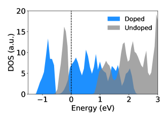
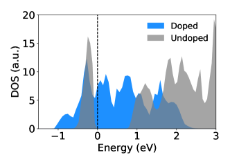
Thus, an investigation of the band structure of the linearized, experimentally observed geometry may shed some light on the nature of this insulating doped phase. Figure 3a illustrates the band structure calculated using the G0W0 method of the doped configuration of Figure 1c. A comparison with Figures 3a and 2b reveals that rather than this structure appearing insulating, the splitting between the original valence and conduction bands of the undoped VO2 structure has vanished completely. The two filled valence -bands which in both the undoped form, and the subsitutionally doped form are separated from the conduction bands now overlap significantly with them. Figure 3b contrasts the densities of states of the undoped and experimentally doped form, and it is clear that the original band gap has completely closed, with a broad peak in the density of states forming which straddles the Fermi level.
This indicates an apparent paradox. If both the undoped and doped structures are experimentally found to be insulating, and standard GW calculations predict a band gap in the undoped form in good agreement with experiment, then the vanishing of any splitting between the bands in the doped form would suggest a transition to a highly metallic state. While the amount of dopant in the structure whose bands are presented in Figure 3a is quite high: 25 %, from a band theory perspective the complete disappearance of the band splitting in the original insulating structure seems totally incompatible with an insulating structure. In addition, the shift of the Fermi level due to the extra valence electron into the broad conduction band suggests that even if any splitting were maintained, such as in the substitutionally doped structure (see Figure 2b), that it would not result in a band insulator.
The reduction in splitting of the valence bands is however compatible with the atomic arrangement of the tetragonal structure. Tetragonal VO2 does not exhibit Peierls pairing of the vanadium atoms, unlike the structures of Figures 1a-b. Instead the vanadium atoms are evenly spaced along the tetragonal c-axis, and are not antiferroelectrically distorted. The local environment of each vanadium atom of the undoped tetragonal structure is identical to experimentally determined environment of the tungsten in doped VO2. Thus this arrangement in the doped structure represents a step back towards the metallic tetragonal form. A resolution of this apparent paradox may be proposed by recognizing that the driving force for the symmetrization may be electron localization of the usual Mott-Hubbard type.
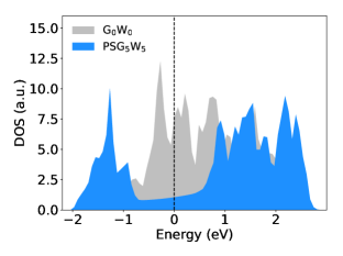
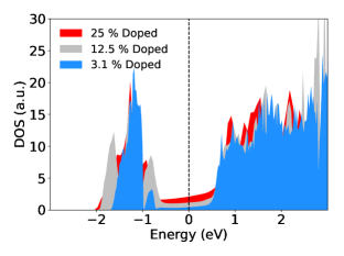
Figure 4 investigates the effect of this by comparing standard G0W0 data with a more strongly correlated PS-G5W5 calculations. Figure 4a compares the densities of states of the standard GW calculation of the experimentally observed structure with a calculation in which strong local k-space correlations are introduced. In comparison to the G0W0 data, the strongly correlated calculation reveals a clear splitting of the density of states into peaks equidistant from the Fermi level. The band structure of Figure 2b reveals that these strong correlations push the empty conduction states up above the Fermi level while the filled states are stabilized in the opposite direction, resulting in the formation of the Hubbard bands. As far as insulating structures go, while some states still exist at the Fermi level, this seems a far more promising candidate.
a b c
This symmetrization of the local environment of the tungsten dopant observed in photoemission experiments Tang et al. (1985); Booth and Casey (2009) (see Figure 1c) can be reconciled by starting from a Mott insulating ansatz. From Figures 2b-c, the most significant effect of introducing a tungsten donor is to dope an electron into the structure, pushing the Fermi level up. From Figure 2a, it is clear that undoped M1 VO2 already has a filled valence band, therefore tungsten doping introduces an electron into the system, creating a partially filled band. If the tungsten atom Peierls pairs with a vanadium atom, the extra electron would interact with both electrons of the Peierls pairing, due to the decrease the hopping energy by reducing the internuclear spacing, and creating potential overlap between the atoms. However if the structure symmetrizes, the two valence electrons on the tungsten atom localize to it, and the single -electron of the vanadium localizes on the vanadium site, reducing interactions. In this respect, this symmetrization is a classic Mott transition; increasing internuclear spacing giving rise to smaller correlations.
The W0.25V0.75O2 doped structure of Figure 4a-c corresponds to a dopant percentage of 25 %, which is much higher than those commonly used to adjust Tc. At this percentage the structure would be expected to be metallic experimentally Tang et al. (1985). Figure 4c explores the effect of reducing the dopant concentration from 25 % through 12.5 % to 3.1 % (scaled such that they integrate to the same total number of states). As the dopant percentage decreases, the density of states at EF decreases concurrently, suggesting that the structure becomes increasingly more insulating as the dopant amount tends to zero, consistent with the fact that fewer carriers are being doped into the structure. This data indicates that at dopant percentages designed to drop Tc to approximately room temperature ( 2-3 % Lawton and Theby (1995)), tungsten doped VO2 will exhibit insulating character.
In summary, by including strong correlations in GW calculations on tungsten-doped VO2 it becomes evident that doping carriers into the band insulating VO2 structure results in a switch to Mott insulating behavior. The added electron occupies the conduction band minima, and strong local correlations in k-space split these minima from the rest of the bands, while a concurrent disruption of the Peierls pairing created by the dopant atom results in them combining with the original valence band into a broad lower Hubbard band. The data suggests that a modification of the pure VO2 structure which results in an increase in electron number will create a Mott insulating defect band in which the Peierls pairing is disrupted, and the structure seeks to minimize correlations by symmetrizing the hopping distances around the defect.
Acknowledgements: SPR and JMB acknowledge the support of the ARC Centre of Excellence in Exciton Science (CE170100026). DWD acknowledges the support of the ARC Centre of Excellence for Nanoscale BioPhotonics (CE140100003). This work was supported by computational resources provided by the Australian Government through the National Computational Infrastructure National Facility and the Pawsey Supercomputer Centre.
Correspondence and requests for materials should be addressed to JMB, email: jamie.booth@rmit.edu.au
References
- Goodenough (1971) J. B. Goodenough, Journal of Solid State Chemistry 3, 490 (1971).
- Wei et al. (2012) J. Wei, H. Ji, W. Guo, A. H. Nevidomskyy, and D. Natelson, Nat. Nanotechnol. 7, 357 (2012).
- Park et al. (2013) J. H. Park, J. M. Coy, T. S. Kasirga, C. Huang, Z. Fei, S. Hunter, and D. H. Cobden, Nature 500, 431 (2013).
- Guo et al. (2011) H. Guo, K. Chen, Y. Oh, K. Wang, C. Dejoie, S. Syed Asif, O. L. Warren, Z. W. Shan, J. Wu, and M. Minor, Nano Lett. 11, 3207 (2011).
- Nakano et al. (2012) M. Nakano, K. Shibuya, D. Okuyama, T. Hatano, S. Ono, M. Kawasaki, Y. Iwasa, and Y. Tokura, Nature 487, 459 (2012).
- Biermann et al. (2005) S. Biermann, A. Poteryaev, A. Lichtenstein, and A. Georges, Phys. Rev. Lett. 94, 26404 (2005).
- Gatti et al. (2007) M. Gatti, F. Bruneval, V. Olevano, and L. Reining, Phys. Rev. Lett. 99, 266402 (2007).
- Wei et al. (2009) J. Wei, Z. Wang, W. Chen, and D. H. Cobden, Nat. Nanotechnol. 4, 420 (2009).
- Lawton and Theby (1995) S. A. Lawton and E. A. Theby, J. Am. Ceram. Soc. 78, 238 (1995).
- Tang et al. (1985) C. Tang, P. Georgopoulos, M. E. Fine, J. B. Cohen, M. Nygren, G. S. Knapp, and a. Aldred, Phys. Rev. B 31, 1000 (1985).
- Marezio et al. (1971) M. Marezio, D. B. McWhan, J. P. Remeika, and P. D. Dernier, Physical review. B 91, 2541 (1971).
- Booth and Casey (2009) J. M. Booth and P. S. Casey, Phys. Rev. Lett. 103, 1 (2009).
- Burke (2012) K. Burke, J. Chem. Phys. 136 (2012), 10.1063/1.4704546, arXiv:arXiv:1201.3679v1 .
- Imada et al. (1998) M. Imada, A. Fujimori, and Y. Tokura, Rev. Mod. Phys. 70, 1039 (1998).
- Anisimov et al. (1991) V. I. Anisimov, J. Zaanen, and O. K. Andersen, Physical Review B 44, 943 (1991).
- Booth et al. (2016) J. M. Booth, D. W. Drumm, P. S. Casey, J. S. Smith, and S. P. Russo, J. Chem. Phys. 244110, 1 (2016).
- Andersson (1954) G. Andersson, Acta Chem. Scand. 8, 1599 (1954).
- Perdew et al. (1996) J. P. Perdew, K. Burke, and M. Ernzerhof, Phys. Rev. Lett. 77, 3865 (1996).
- Blochl et al. (1994) P. E. Blochl, O. Jepsen, and O. K. Andersen, Phys. Rev. B 49, 16223 (1994).
- Monkhorst and Pack (1976) H. J. Monkhorst and J. D. Pack, Phys. Rev. B 13, 5188 (1976).
- Shishkin and Kresse (2006) M. Shishkin and G. Kresse, Phys. Rev. B 74, 35101 (2006).
- Shishkin and Kresse (2007) M. Shishkin and G. Kresse, Phys. Rev. B 75, 235102 (2007).
- Kresse and Furthmüller (1996) G. Kresse and J. Furthmüller, Phys. Rev. B 54, 11169 (1996).
- Shin et al. (1990) S. Shin, S. Suga, M. Taniguchi, M. Fujisawa, H. Kanzaki, a. Fujimori, H. Daimon, Y. Ueda, K. Kosuge, and S. Kachi, Phys. Rev. B 41, 4993 (1990).