Construction and commissioning of a technological prototype of a high-granularity semi-digital hadronic calorimeter
Abstract
A large prototype of was designed and built as a demonstrator of the semi-digital hadronic calorimeter (SDHCAL) concept proposed for the future ILC experiments. The prototype is a sampling hadronic calorimeter of 48 units. Each unit is built of an active layer made of Glass Resistive Plate Chamber (GRPC) detector placed inside a cassette whose walls are made of stainless steel. The cassette contains also the electronics used to read out the GRPC detector. The lateral granularity of the active layer is provided by the electronics pick-up pads of each. The cassettes are inserted into a self-supporting mechanical structure built also of stainless steel plates which, with the cassettes walls, play the role of the absorber. The prototype was designed to be very compact and important efforts were made to minimize the number of services cables to optimize the efficiency of the Particle Flow Algorithm techniques to be used in the future ILC experiments. The different components of the SDHCAL prototype were studied individually and strict criteria were applied for the final selection of these components. Basic calibration procedures were performed after the prototype assembling. The prototype is the first of a series of new-generation detectors equipped with a power-pulsing mode intended to reduce the power consumption of this highly granular detector. A dedicated acquisition system was developed to deal with the output of more than 440000 electronics channels in both trigger and triggerless modes. After its completion in 2011, the prototype was commissioned using cosmic rays and particles beams at CERN.
keywords:
Keywords: Glass RPC; Calorimeter; ILC; embedded electronics; power-pulsing1 Introduction
The success of future high-energy experiments intended to investigate physics phenomena in the TeV range will be determined by their ability to measure precisely the energy of jets associated with the production of bosons such as . Among the different proposed methods to obtain high-precision jet energy measurements, one of the most attractive techniques is based on the Particle Flow Algorithm (PFA) approach [1, 2]. In this approach, particles are to be followed in the different sub-detectors and their energy or momentum to be estimated in the sub-detector which provides the best resolution of such a measurement. For the PFA techniques to be successfully and efficiently applied, electromagnetic and hadronic calorimeters need to have tracking capabilities, in addition to their usual role of energy measurement. This could be achieved by designing a new generation of sampling electromagnetic and hadronic calorimeters with high-granularity in both the transverse and the longitudinal directions
The challenge of this new generation of calorimeters is to cope with the millions of electronic channels needed to read out such a high-granularity and yet still compact and hermetic detector. To address the compactness and power consumption, genuine designs are needed. The SDHCAL prototype, whose development is also a part of the CALICE collaboration activities to study highly granular calorimeters, has successfully achieved these contradictory requirements.
After a general description of the SDHCAL prototype we describe the GRPC detector developed for this prototype in the third section. The new electronic readout is detailed in the fourth section. In the fifth and the sixth sections the hardware and the software developed for the acquisition system are respectively described. The seventh section depicts the cassette structure used to assemble the different components of the active layer as well as the self-supporting absorber mechanical structure to host the cassettes. In section eight a description of event building, data quality control and detectors performance is given. Finally the technical performance of the SDHCAL prototype are summarized in section nine.
2 General description
The basic unit of the SDHCAL is made of a cassette containing the active layer. The latter is composed of a GRPC detector and its embedded readout electronics. The cassettes are inserted into a self-supporting mechanical structure made of thick plates of stainless steel. This structure forms a robust frame to host the cassettes on the one hand and constitutes the essential part of the hadronic calorimeter’s absorber on the other hand. The cassette walls and the structure plates are made of the same material and thus complete the calorimeter’s absorber. In total of stainless steel is separating two consecutive active layers.
A simple cooling system made of two thin boxes ( width) each covering one lateral side of the prototype is used. A water circuit inside the two boxes allows to absorb part of the heating produced by the electronic readout system. This cooling system will not be necessary when the power-pulsing scheme will be operated in ILC power cycle schemes. However in beam test conditions (longer data taking cycles) this was found helpful to stabilize the temperature of the GRPC detectors during data taking. A dedicated system to produce the gas mixture needed to operate the GRPC was conceived to feed in parallel the different GRPC of the prototype. The prototype is also equipped with a high voltage system to polarise the GRPC individually. Finally, the data collected by the active layers are treated by an acquisition system that was developed for this purpose.
3 GRPC construction
3.1 GRPC description
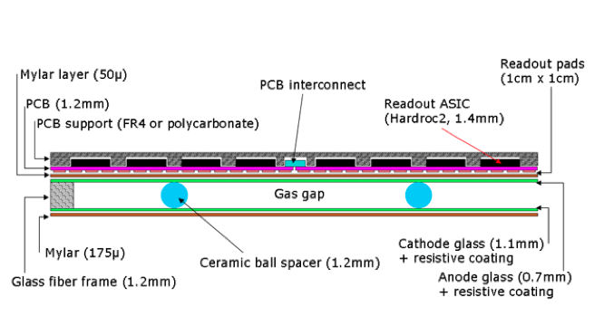
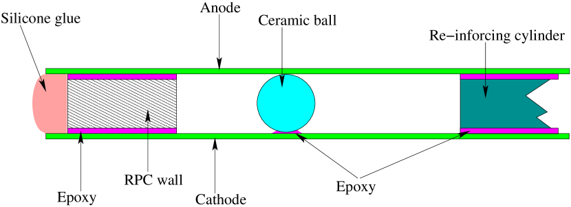
The GRPC developed for the SDHCAL is made of two glass plates with a thickness of for the one associated to the anode and for that associated to the cathode. The two plates are separated by a space which is maintained constant thanks to special spacers (Figure 1). The distance and the size of those spacers were optimized to eliminate the detector dead zones while providing a uniform electric field between the two plates. The two glass plates are covered on their outer face by a conductive painting. This allows to apply high voltage polarization to create an electric field in between. The gap between the two plates is filled with a gas mixture of TetraFluoroEthane(93%), CO2(5%) , SF6(2%). The first gas provides the primary electrons-ions when ionized by the crossing charged particle while the second and the third are UV photons and electrons quencher respectively. Their role is to limit the size of the avalanche that follows the creation of primary electrons. It also reduces the probability of producing additional avalanches away from the charged particle impact in the GRPC. It is worth mentioning here that both TetraFluoroEthane and SF6 are not eco-friendly. Their use in future detectors could be questioned. Therefore, attempts to replace them by new gases with similar functionalities but with much lower Global Warming Potential index are being currently made. To replace the TetraFluoroEthane for instance, new refrigerant gases proposed by car industry like the HFO-1234yf are being investigated.
The gas tightness is provided by a robust insulating frame made of glass reinforced epoxy laminate (Veronite FR-4). This frame is only wide leading to a dead area of the detector of less than 1.3%. A gas distribution system was also developed. It allows to renew the gas content of the chamber in an efficient way taking into consideration the fact that gas inlets and outlets are to be on one side of the chamber. The system is designed to reduce the gas consumption. This and the recycling progress achieved by the RPC-gas group at CERN, are important elements to reduce the cost of the gas consumption of such hadronic calorimeters in the future experiments.
3.2 Chamber design
The chambers consist of the elements shown in Figure 1. Precision ceramic (Zr O2) balls of diameter are used as spacers to separate the two electrodes: the anode ( thickness) and the cathode ( thickness). Readout pads of area are isolated from the anode glass by a thin Mylar foil. These pads are etched on one side of a PCB; on the other side are located the front-end readout chips. Finally, a polycarbonate spacer (‘PCB support’ in Figure 1) is used to ‘fill the gaps’ between the readout chips and to improve the overall rigidity of the cassette (detector/electronics ‘sandwich’) as well as the lateral homogeneity of the active layer. The total theoretical thickness of the assembly is . Taking into account air gaps and engineering tolerances, the true thickness was found to be slightly bigger but not exceeding .
3.3 Resistive coating
To identify the best resistive coating for the chamber glass different products were tested. All of them providing surface resistivity in the range
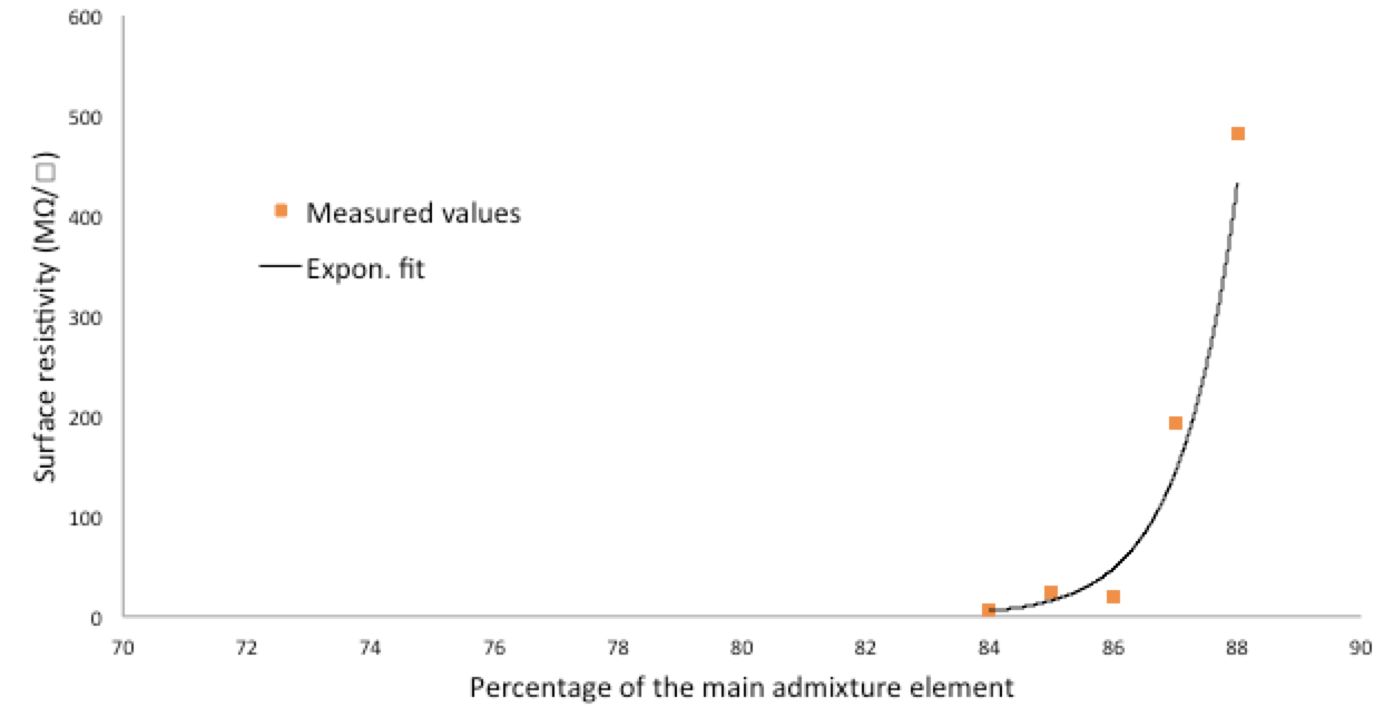
One of the commercial products we tried, the Licron, was found to be problematic in that it has the tendency to ‘migrate’ away from the high voltage strip glued to the cathode glass, resulting in loss of the HV contact after a very short time (a few days of continuous use). We have constructed several large-area GRPC using another commercial product (Statguard), an inexpensive floor paint used in electrostatic discharge (ESD) applications. These chambers have been successfully operated [4]; however the paint was applied to the glass using a paint brush, which is found not suitable for mass production. Attempts to coat large areas with Statguard using the silk screen technique produced unsatisfactory results. In addition, this product also has a long time constant to reach a stable surface resistivity (typically two weeks). Research was therefore carried out to find a product specifically designed for silk screen printing with the correct surface resistivity. Two products were identified, both of which are based on colloids containing graphite. One of these products is a single component paint with a dry surface resistivity of after being deposited using the silk screen method. The second product comes as two components which must be mixed by the user. The surface resistivity may be adjusted over a wide range by changing the mix ratio (Figure 2). Both products require baking at around 170oC to attain a stable surface resistivity.
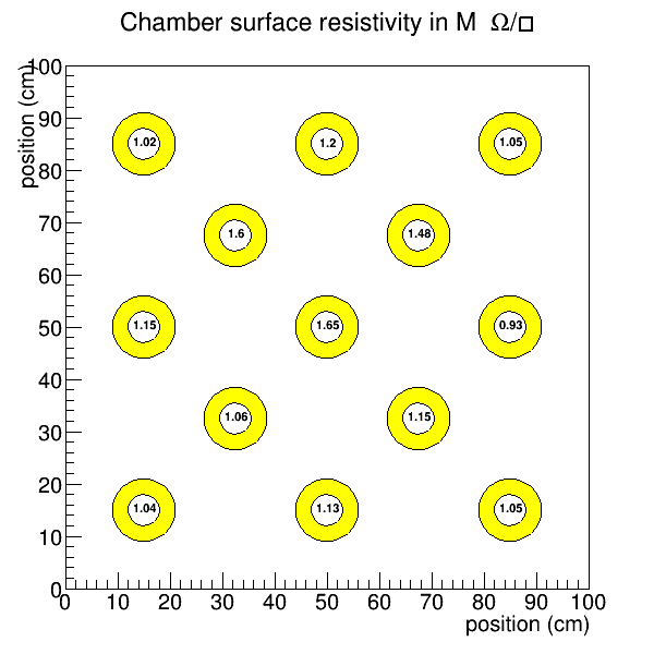
The measured surface resistivity at various points over an early example of a glass coated with the bi-component paint are shown in Figure 3. The mean value is and the ratio of the maximum to minimum values is 1.8. A study was also made of the repeatability of the surface resistivity between different mix batches. It was found that surface resistivity in the range could be reliably reproduced, again with a factor of approximately two between minimum and maximum values. These results are considered entirely satisfactory, since it is known from previous tests [4] that significant impact on chamber performance begins to be measurable only for resistivity variations of the order of a factor 10.
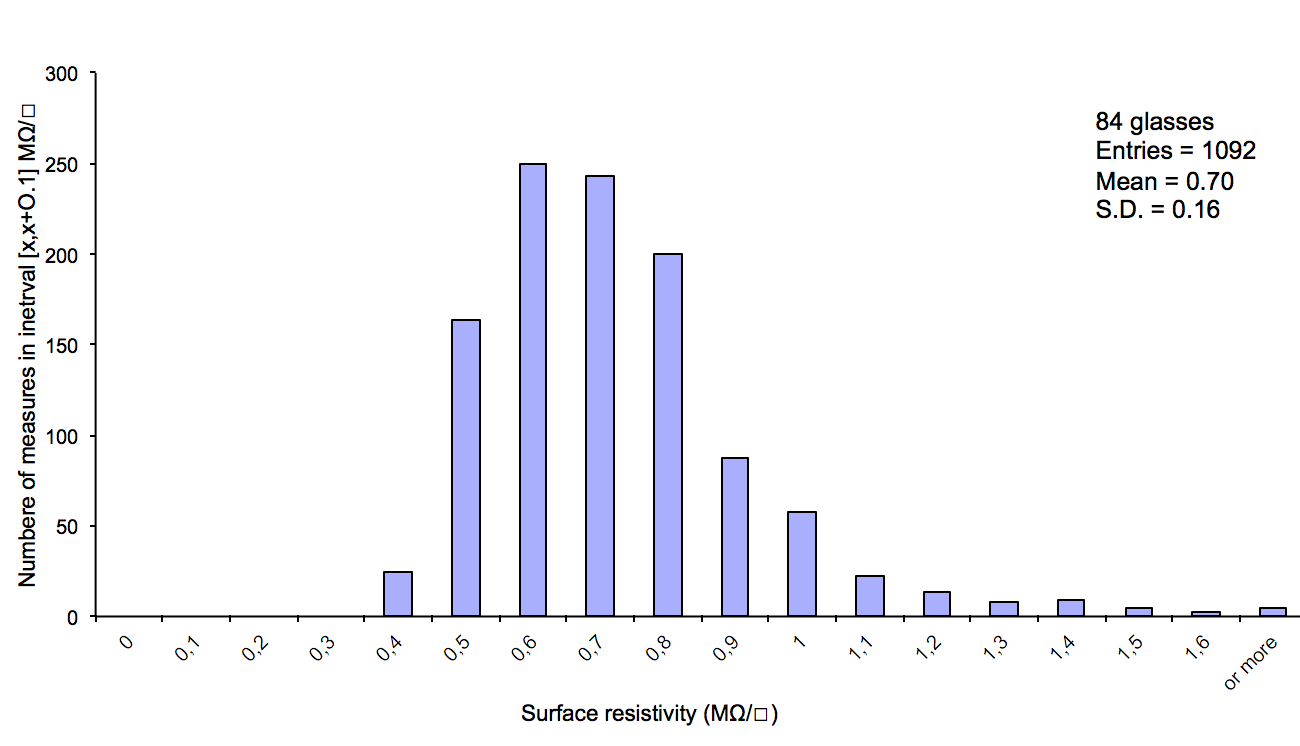
Indeed for the majority of the production glasses, a slightly lower surface resistivity was chosen; Figure 4 shows the distribution of average values for 84 glasses. The repeatability of the coating process is well demonstrated, the standard deviation of the distribution being for a mean of .
Electrical contact to the paint layer is made by means of copper tape with conductive adhesive. The adhesive was chosen so it has no chemical interaction with the coating components in order to avoid the migration of the painting molecules away from the high voltage contact and to ensure a long term contact stability222After three years of running no loss of high voltage connection was observed in the 48 GRPCs of the prototype..
3.4 Spacer distribution
A finite element calculation was made to determine the optimum distance between the gas gap spacers (ceramic balls). The goal of this study was to maintain a constant distance between the two electrodes ensuring the same electric field and hence the same gain in all the GRPC chamber while introducing the smallest dead zone. Two static forces acting on the glass plates were considered: the weight of the anode plate (chamber horizontal) and the electrostatic force between the plates for a potential difference of (maximum likely chamber voltage). The results of the simulation (Figure 5) indicate that a maximum glass deformation of 44 microns occurs for a ball spacing of . This maximal deformation333The opposite force produced by the slight excess of the pressure inside the chamber with respect to the outside atmosphere was not taken into account. was considered acceptable in terms of the computed gain variation due to the non-uniformity of the gas gap height.
3.5 Distribution of gas within the chamber
Gas distribution within the RPC is improved by channeling the gas along one side of the chamber and releasing it into the main gas volume at regular intervals. A similar system is used to collect the gas at the other side of the chamber. A finite element model has been established to verify the gas distribution (see [4] for details). Results from this model are shown in Figure 6. The simulation confirms that the gas speed is reasonably uniform over most of the chamber area and that this design significantly improves the distribution of gas with respect to a chamber with no gas channels. A profile of the quantity known as the ‘Least Mean Age’ (LMA) was also generated by the model. This is defined as the time for gas to reach a given point in the chamber after entering the volume, including the effects of diffusion. At most points in the chamber the LMA was calculated to be around . When compared with the estimated gas speed shown in Figure 6, the LMA value indicates clearly that diffusion plays an important role in the distribution of the gas.
3.6 Mechanical assembly
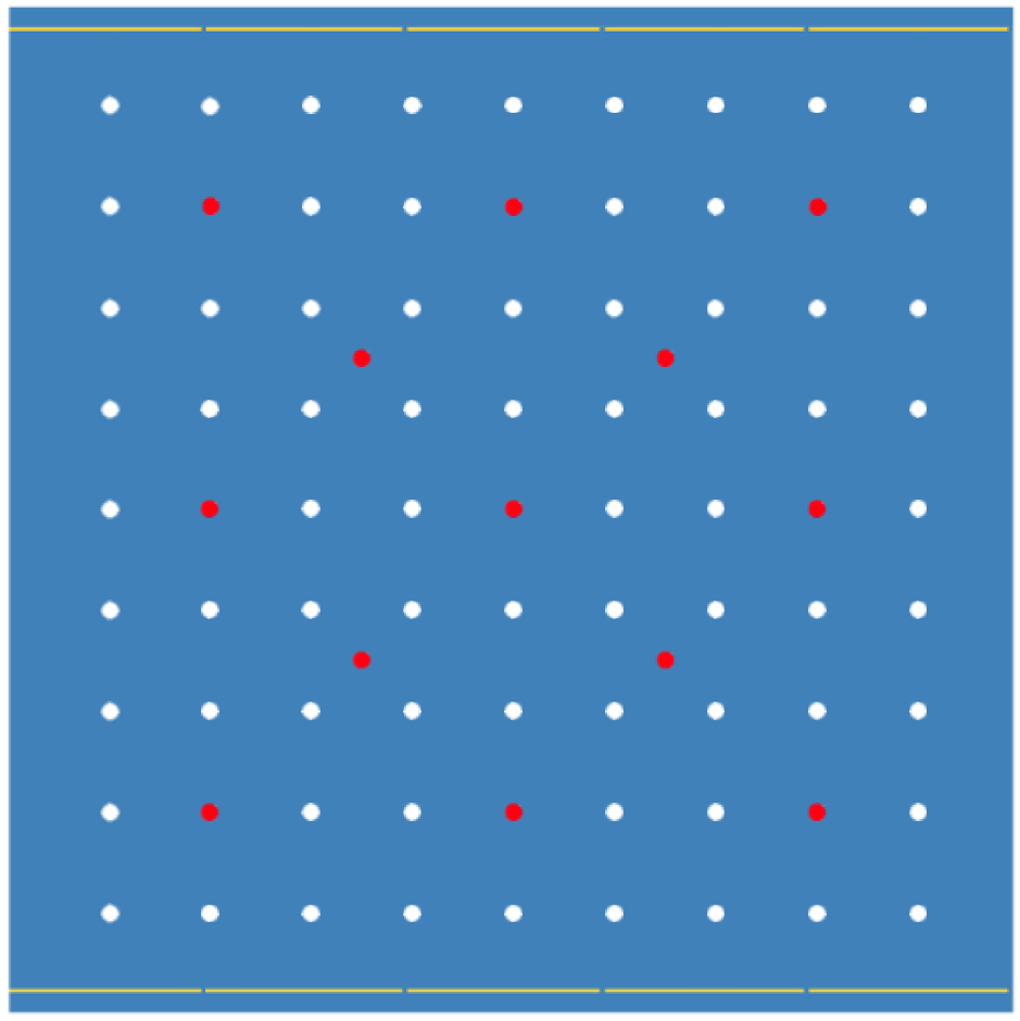
The glass plates are soda-lime float glass with a bulk resistivity of . Assembly of each chamber begins with the cathode glass supported paint side down on a flat support (aluminium honeycomb plate). The gas gap spacers are then glued onto the glass at 85 locations using Araldite 2011 epoxy (Figure 7). The majority of the spacers (white dots) were the ceramic balls mentioned above, but in 13 locations (red dots) the spacers were diameter Vetronite G11 cylinders precision machined to a height of . These spacers, which provide a greatly increased gluing surface compared to the ceramic balls, were added to improve the robustness of the assembly and maintain the assembly integrity when the absence of High Voltage does not balance the overpressure needed for gas flowing. Our choice of using these two kinds of spacers was motivated by the attempt to reduce the dead zone percentage as much as possible and still have a robust structure. Ceramic balls, glued to one electrode, allow to keep the distance between the two electrodes constant while introducing negligible dead zone. The dead zone introduced by cylindrical spaces is sensibly higher but allow more robustness since they are glued to both electrodes.
The gas channelling system consists of short lengths of PMMA fibers (diam. ) that are glued to the glass end-to-end, with small gaps through which the gas is allowed to escape into the chamber (yellow lines on each side of Figure 7).
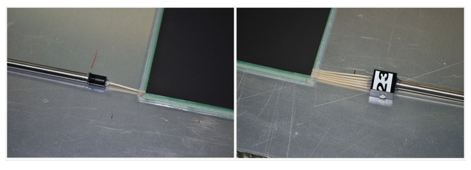
The gas volume is closed by gluing G11 strips () around the perimeter of the glass. On one side of the chamber, gaps are left at two locations into which capillaries are glued to allow direct injection / removal of the gas mixture into / from the channelling system. The capillaries have external diameter with a wall thickness. A single capillary is used for the inlet whereas the outlet consists of 5 capillaries to minimize the pressure drop (Figure 8), thus minimizing the pressure inside the chamber. Outside of the chamber, the capillaries are adapted to short lengths of stainless steel pipe for easy connection to standard gas fittings. In the case of the outlet, where 5 capillaries must be grouped together, a custom adaptor was produced in-house (numbered connector in Figure 8).
The assembled cathode glass is transferred to a pivoting table and glue applied to the upper surfaces of the chamber frame, the cylindrical spacers and the walls of the gas channels. The table is rotated to the vertical position and the anode glass is mated to the gluing surfaces in this position (the glass plates may be handled manually without supports when vertical). A lip on the lower edge of the pivoting table allows precise alignment of the anode and cathode glasses. The whole assembly is then returned to the horizontal position and the glue is allowed to dry. Weights are placed above the gluing points during the curing period.
The G11 strips forming the chamber frame are recessed by to allow the later application of a bed of Dow Corning 3140 silicone glue around the perimeter of the chamber for additional gas tightness. A summary of the gluing scheme is given in Figure 9.
4 Electronics readout
4.1 ASIC
HARDROC (HAdronic Rpc Detector ReadOut Chip) is the very front end chip (Figure 10) that was designed for the readout of the RPC detectors foreseen for the Semi-Digital HAdronic CALorimeter (SDHCAL) of the future International Linear Collider. It has been designed in SiGe technology. There have been two versions of this ASIC : (HARDROC1 [5] and HARDROC2 [6]). The main difference between these two versions is the package which is a 1.4 mm thick plastic Thin Quad Flat Package with 160 pins (TQFP160) for HARDROC2 instead of a 3.4 mm thick Ceramic Quad Flat Package with 240 pins for HARDROC1 (CQFP240). The thin package is more suitable to be embedded inside the detector. It is the HARDROC2 version that was used in the SDHCAL prototype construction.
The HARDROC readout is a three-threshold (semi-digital) one that integrates on-chip data storage functionality. Each of the 64 channels of HARDROC (Figure 11) is made of a fast low-input-impedance current preamplifier with a 8-bit precision gain tunable between 0 and 2, followed by 3 variable gain fast shapers (FSB) connected to 3 low-offset discriminators. The threshold of one is set to a low value, that of the two others to medium and high values in order to auto-trigger down to and up to . This auto-triggering mode allows reducing the data volume by recording only signals compatible with those produced by the passage of charged particles in the GRPC. The 3 discriminator outputs are encoded into 2 bits which are stored in a 127 deep digital memory. Also recorded, the bunch crossing identification which is coded using a 24 bits counter (ASIC BCID). This internal digitization implies that only digital data are taken out. To minimize the number of lines between ASICs, they have been designed to be daisy chained and read out sequentially during the readout period. To reach a power consumption of , the ASIC has been designed to be power pulsed and a Power-On-Digital (POD) module for the 5MHz and clocks management during the readout phase has been integrated. 872 configuration registers with default values are integrated to set the required configuration. These configuration parameters are referred as Slow Control (SC) parameters here after.
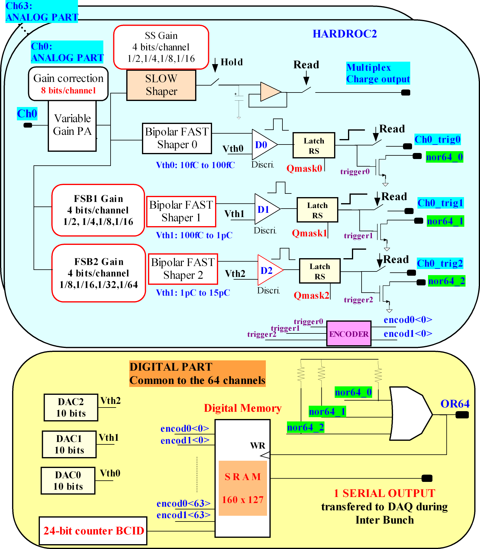
4.1.1 Trigger path
The trigger path is made of the input preamplifier followed by 3 fast
shapers (with a peaking time tunable between 15 and 30 ns), each followed by three discriminators. The fast shapers are
designed around a band-pass architecture and are referred as FSB0, 1 and
2 for Bipolar Fast Shaper below. FSB0 is dedicated for input charges
varying from up to a few hundreds of fC, FSB1 for input charges
from up to , and FSB2 for input charges from up to .
The feedback network of each shaper can be changed independently
thanks to the SC parameters allowing peaking times between 15 and and also a variable gain. The gain of FSB0 is typically about
using a feedback resistor of and a feedback capacitor of
. This gain can be varied by a factor of 4. The gain of FSB1 and FSB2 can be varied using their
variable feedback network and also a 4-bit current mirror gain. The
output of each shaper is connected to a low offset comparator. The
comparator reference levels (thresholds) are set using three
integrated 10-bit Digital Analog Convertors (DAC) allowing the
settings of the thresholds in the 0-1023 DAC units range. The slope is
unit which corresponds typically to unit for
FSB0.
Finally, to estimate precisely the conversion factor between the injected charge and the DAC value of a given threshold for the three FSB, a scan of charge injection was performed in the range for which the FSB response is linear. For each injected charge and for one of each of the thresholds a scan of the threshold values is performed and the efficiency of each channel is measured by repeating the injection many times. In absence of electronic noise this curve should be a perfect step function but the efficiency curve obtained experimentally is not. It has a shape of inverse S and is commonly called the S-curve. It represents indeed an Erf function and hence the threshold value in DAC units corresponding to the 50% efficiency of the curve is used to determine the value of the injected charge in the DAC units. Taking advantage of the linear behavior of the FSB in the studied range of charge, a linear fit of the various points obtained by the scan gives the conversion factor between the injected charge and the DAC. This operation is repeated for the the three FSB. For instance, the linear fit of the response of FSB0 of one channel is shown in Figure 12. In this case the conversion factor was found to be : 1 DAC Unit = 0.8 * Qin ().
4.1.2 Internal digitization
For each of the three comparators, a logic OR is made of the 64 channels. By Slow Control, the user can select which of the 3 OR should be used to trigger the digital part of the ASIC. The status of the selected OR is evaluated by the common digital part. If one of the 64 comparators of the selected OR is fired, the data are stored in the memory. Each comparator output can be masked by Slow Control to avoid fake triggers due to a noisy channel. This is known as the "auto-triggering" scheme. The ASIC can store up to 127 frames in its internal memory. A frame stored in one ASIC consists of a hit map of the 64 channels with 2 bits per channel plus a time stamp of 24 bits and an 8-bit chip identifier. The Gray-coded time stamp is derived by a 5MHz clock.
Each channel of the ASIC integrates for each channel a test capacitor of with a precision of (given by the technology). This calibration capacitor is used to calibrate the response of each channel. The cross-talk between adjacent channels was measured by injecting an electric signal of through one channel. The signal observed in the other channels was found to be less than 2% of the injected charge. About 0.5% of this crosstalk is given by the analog part of the electronics, the rest is given by the proximity of the other detector cells. This 2% crosstalk is low enough for this semi-digital readout as the lowest threshold of the three discriminators is always set to more than 100 fC. The effect of such cross-talk is thus limited to cases when large charge is deposed in one pad () but this scenario takes place in the core of the hadronic and electromagnetic showers for which the adjacent pads are very often fired at the same time due the presence of many charged particles in the shower core.
The communication between the ASIC and acquisition system (DAQ) acts in two steps: an acquisition phase and a readout phase. The acquisition phase is stopped at the end of the acquisition window or when a full-memory state (RAMfull) is reached. Then, triggered by an external signal provided by the DAQ, the second phase starts: after receiving the StartReadout signal, the first ASIC enters its readout phase and issues an EndReadout upon completion. The latter is transmitted to the next ASIC which interprets it as a StartReadout command. To read out large GRPC detectors with a lateral resolution many ASICs need to be assembled together. To limit the number of wires between the ASICs and the DAQ system the digital readout signals are connected with an open collector bus per board and daisy-chained in a ring topology, leading to use only one wire for the link. Similarly, a daisy-chained ring bus is used for the assignment of the SC parameters to all the ASICs of one board. The situation is different for the acquisition phase where all the ASICs should start at the same time. In this case, a StartAcquisition command is broadcasted to all the ASICs to initiate this phase. Broadcasting signals are sent to all the ASICs in parallel. All the commands sent to the ASICs by the DAQ are controlled by an FPGA device ( more details in section 5.1).
To avoid inherent problems related to the daisy-chained system which could result in losing control over a whole branch of the readout system, a redundancy system was implemented. The system uses two readout buses (one is designed as the default and the other as the spare bus) with the possibility to select one bus or the other through the configuration parameters of each ASIC. In case of an ASIC (number N in the chain) is found faulty on the default bus, the chain is then repaired as follows:
-
•
ASIC number N-1 is configured to get its data on its default bus and to output its data on its spare bus.
-
•
ASIC N is configured to use its spare bus (both for input and output data).
-
•
ASIC N+1 is configured to use its spare bus for the input and the default one for the output.
This works as long as two consecutive ASICs are not faulty and the spare bus of the ASIC number N is still operational.
It is worth mentioning here that a more robust design is foreseen for the next generation of the HARDROC ASIC. Two I2C (selectable by external programmable means for each ASIC) buses will be used for the configuration parameters transmission. This is intended to eliminate the possible problems related to the use of daisy-chain technique to configure the ASICs.
4.1.3 Power-pulsing mode
Since the ILC duty cycle is expected to be one millisecond bunch crossing every 200ms, the HARDROC was conceived to take advantage of such a scenario using the power pulsing mode thanks to a special module called Power-On-Digital (POD). This consists of switching off the internal bias currents of the various ASIC channels during the inter-bunches whereas the power supplies are kept on. There are 3 Power-On signals: Power-On-Analog (controlling the analog part), Power-On-Digital (controlling the clock-gating) and Power-On-DAC (controlling the setting of the discriminators thresholds). Each of them can be forced through the parameters of the Slow Control configurations.
4.1.4 ASIC production and control
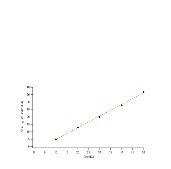
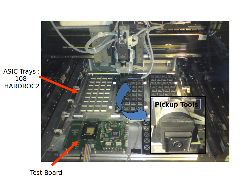
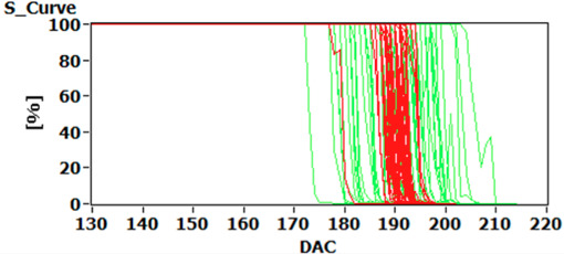
To equip the 48 detectors of the SDHCAL, 6912 ASICs are needed. More than 10500 ASICs were however produced. They were tested and calibrated using a dedicated tool. The tool consists of a robot allowing to pick up one by one the ASICs placed in a special tray containing up to 108 ASICs and to plug them in a test board (Figure 13) conceived for this purpose. A pattern recognition system using a camera allows to guide the robot to achieve this step. Once the ASIC is well placed, the proper test then starts using a Labview application that was elaborated with the purpose to realize all the tests and the calibration operations automatically. The tests allow to check that all the channels of one ASIC are operational. This consists of checking the response of the three comparators associated to the three thresholds for a given injected charge. ASICs for which the 64 channels and their three comparators are found to be operational are then calibrated and replaced in their original place in the tray. The calibration operations are realized as follows: a scan of the first threshold is performed by injecting the same charge of in one given channel after selecting the first threshold value in terms of DAC. is a typical threshold value used to read out GRPC chambers. The operation is repeated for a large range of DAC to allow the construction of the so-called S-curve (Figure 14). The same operation is performed for different electronics gain of the first comparator.
The 50% trigger efficiency point of each channel is extracted by fitting the S-curves with a sigmoid function. The dispersion of this 50% trigger efficiency point gives the dispersion between channels for a given gain. As illustrated in Figure 14, this dispersion can be reduced to a few percent by tuning the gain of each pre-amplifier individually. In this way all the channels have their 50% efficiency at almost the same point for a given threshold.The gain corrections are then recorded in a dedicated data base for future use.
The whole batch of ASICs was tested and calibrated with a rate of 200 ASICs per day. A yield of 93% was observed. It corresponds to ratio of ASICs which are fully operational.
4.2 Active Sensor Unit
The Active Sensor Unit (ASU) is the electronic board that hosts the different electronic readout components. In the SDHCAL prototype the ASU was conceived to cope with the Daisy chain scheme. It contains all the connections allowing the transmission of the different signals between the ASICs as well as those between the ASICs and the acquisition board. The ASU hosts also the pads of which are to be in contact with the GRPC detector.
4.2.1 ASU structure
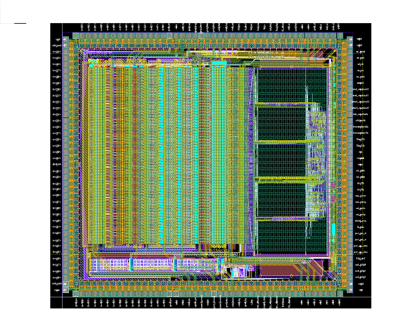
To read out the GRPC detectors of the SDHCAL, ASUs of the same size () are needed. Feasibility constraints make the tasks of circuit production, components soldering, testing and handling of the assemblies, exceedingly difficult in the case of a single PCB of one square meter. The solution of dividing that circuit in 6 more manageable ASU boards was adopted and is schematically shown in Figure 15.
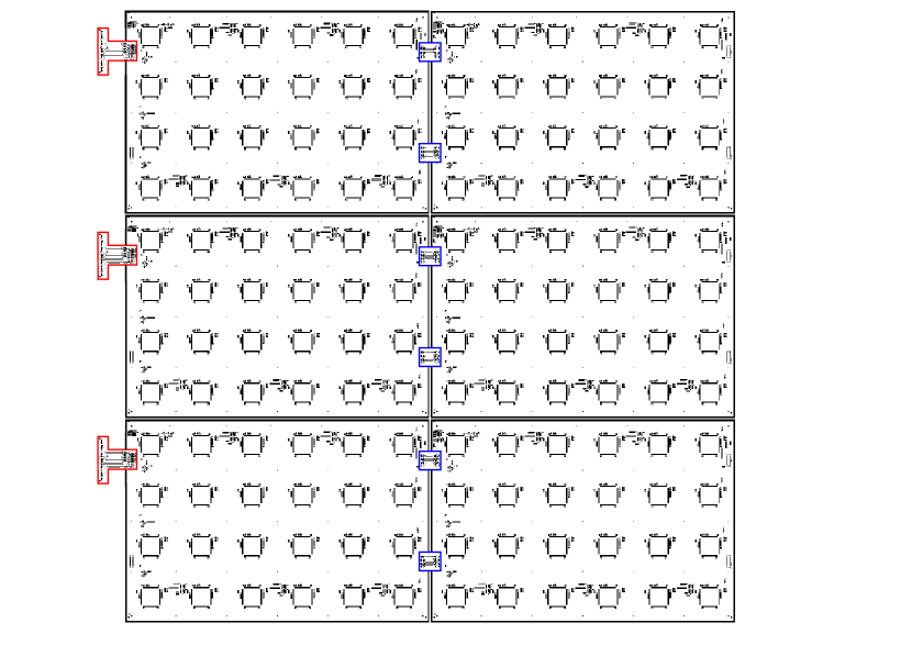
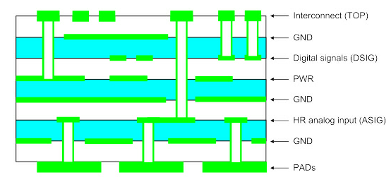
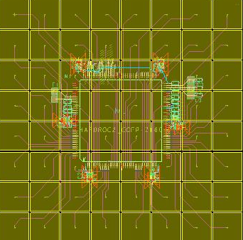
Each of the six ASUs has been designed to host 24 ASICs. The pads coupling the GRPC chamber with the front-end HARDROC must be laid out on the bottom layer of a PCB without other components and vias. This, with the added constraint of keeping the thickness of the electronics assembly to a minimum, poses the problem of routing both the ASIC analog input signals and the digital clocks in order to minimize crosstalk. A solution based on an 8-layer integrated circuit, with blind and buried vias, using the stacking diagram is shown in Figure 16. The designed base pattern of 64 square pads arranged in a 8 x 8 matrix (Figure 17), has been adopted. To reduce cross-talk, adjacent pads are separated by a space of 406 microns. As described in [3], this space is not a dead one since the passage of a charged particle in this could be detected thanks to the charge induction in the the adjacent pads. The routing of each input signal from one pad up to the ASIC pin has been carefully optimized to reduce the crosstalk: all input signals are laid out in the same analog signal layer (ASIG in Figure 16) which is sandwiched between two GND layers. Great care has been taken to keep the routing of digital signals well separated from the vias connecting signals in ASIG to the TOP layer. The HARDROC base pattern is then replicated 24 times in the boards following a form factor. Furthermore, the form factor chosen for the ASU board makes it possible to use a single Detector InterFace (DIF) board to control a set of 48 HARDROCs: the pair of two ASU boards (called a slab) is then powered through the same DIF board and a complete square meter of front-end electronics requires 3 DIFs.
One of the main challenges in the design of the ASU board relies on the routing of the LVDS and single-ended digital control signals while keeping their distribution tree well balanced along the slab. The LVDS control signals issued by the DIF board are buffered in a separate interconnect board (DIF-ASU) for each slab of two ASU boards. Those as well as other signals, together with the power supply, need to be passed to the second ASU board in the slab. The interconnect solution adopted for the board is shown in Figure 15: 2 ASU-ASU boards (outlined in blue) interconnect the signals of the same slab (there are 6 per 1m2), while one DIF-ASU (outlined in red) for each slab connects the slab to the DIF board (there are 3 SIF-ASUs per 1m2). The main constraint in the design of such interconnects relies in keeping the total thickness of the assembly within so it does not exceed that of the HR2 package: this has been achieved using a pitch board-to-board connector with stacking height. The ASU board uses four receptacle connectors on its two short sides in order to allow the interconnection with the DIF and with a second ASU board.
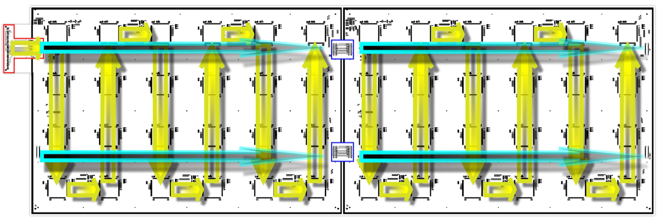
Figure18 shows the routing distribution flow of the HARDROC control signals all along the slab: the slow-control signals proceed connecting the ASIC column wise, with the possibility foreseen on the board of being buffered at each column of 4 ASICs. Actually, two buffers are placed on each ASU : one at the beginning of the SC line and the other at its end. The LVDS signals (the 40 MHz readout clock amongst them) are routed instead along differential lines interconnecting 6 ASICs each, which are terminated on the second board of the slab.
4.2.2 ASU production and quality control tests
A pre-production run of 20 PCB has been required to the manufacturer in order to primarily assess the required planarity under production conditions. Three of those PCB has then been fully populated with 24 HARDROCs, connectors and components and the assemblies tested in a validation test-bench. Again, production-like conditions were asked to the assembly manufacturer, in order to assess the critical capability of maintaining the correct alignment tolerances between the connectors throughout the full production run. A positioning tool has been built by the manufacturer in order to prevent any misalignment of the four board-to-board connectors during the solder reflow process while an assembly tool testing the mechanical tolerances of the populated board assembly has been used for validating the pre-production. The validation test-bench has been developed and refined to assess the production process and has been used throughout the mass production to check out each assembled ASU. It consists of a GRPC detector in a steel cassette and its HV supply with the necessary setup for reading out the data produced by one ASU and then by a full slab of 48 HARDROCs. An acquisition DIF board connected to a PC with an adapted version of the DAQ software collects for each ASU the data generated by the 24 HARDROCs, triggered only by the noise, until an adequate statistics is collected. The analysis software rejects any board showing more than 20 total channels dead (i.e. collecting no data) or more than 5 dead channels on the same HARDROC. All the ASUs produced by the manufacturer are in a test-only configuration allowing the readout of the 24 ASICs: after a board has been validated for the integration into the SDHCAL, it is reconfigured as one of the two possible configurations used within a slab of two boards. The assembly consisting of two ASU boards and two interconnecting boards (ASU-ASU) is then tested again checking the connectivity between the ASUs: the four boards are labeled together to be integrated into a square meter circuit as part of the same slab. A square meter assembly consists of three slabs soldered together: in order to respect the dimensional tolerances of the assembled board, a framing support has been manufactured allowing the correct relative positioning of the 6 ASU composing the 3 slabs before their soldering. Only ASU boards having been checked out with the production test-bench are integrated in a square meter assembly: the boards failing this preliminary test are labeled as faulty and enter a debug phase.
The faulty ASUs are due to problems related to the ASIC or to the ASU assembly. Completely failing ASICs and pin-soldering faults preventing the correct functional of some ASICs were the most common in the first category. The faults falling into the second category concern shorts and opens found on the assembly, mainly at board-to-board connectors pins.
Less than 1% of the 306 manufactured ASU boards failed to pass the test-bench and needed some kind of debug and repair: the largest percentage of those faults was brought by ASICs failing after having been assembled on the boards. This large number of failing ASICs (53/7344), taking into account that all the HARDROCs used for the integration were previously tested in a dedicated chip-level test-bench, require an explanation. Indeed, no Burn-In strategy has been adopted during the manufacturing. In the first part of the board assembly production the packaged ASICs were sent to the manufacturer after a prolonged period of non-dry storage and then they were submitted to the reflow soldering without a previous baking for moisture removal. The introduction of a baking routine has cured almost completely the problem of failing ASICs. The adoption of a lead-based soldering has completely solved the problem with the pin-soldering problem.
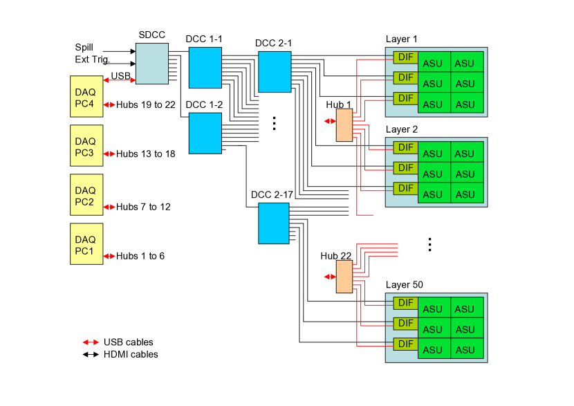
5 The SDHCAL data acquisition hardware
The general architecture of the acquisition system hardware is shown
in Figure 19. The DAQ is connected to the computer network in
two ways: the first one allows to manage the system synchronization
using HMDI transmission protocol and the second one, using a USB
transmission protocol, is responsible for SC configurations and the data transmission. The Synchronous Data Concentrator Card
(SDCC) manages the synchronization of the system. It receives commands
from the computer network and sends them synchronously using private protocol on HDMI cables, to the different Detector InterFace boards (DIFs),
which are connected to the detectors (see next subsection). The limited number of the SDCC HDMI
outputs (9 outputs) made it necessary to use additional boards called Data Concentrator Cards (DCCs).
They are used as FAN IN/OUT devices to send the commands to a large number
of DIFs but with one level of DCC (9 of them) with each having 9 HDMI outputs also, only 81 DIFs could
be connected to the DAQ. Since each active layer of the the prototype
needs 3 DIF to be read out, only 27 cassettes could thus be connected to the
DAQ with one level of DCC. In order to operate the totality of the
prototype units, a second level of DCC was added. This allows to read out
up to 729 DIF corresponding to to a number of 243 SDHCAL layers exceeding largely the needed number for the prototype’s layers.
To operate the DAQ system, only one PC is needed to send the commands to the SDCC
while several PC are used to receive the data. In the following we give a detailed description of the different boards used in the acquisition
system and their functionalities.
5.1 Detector InterFace(DIF) card
5.1.1 DIF architecture
The general architecture of the DIF is shown in Figure 20. The DIF intelligence is based on an Altera FPGA Cyclone 3. The FPGA is connected through USB and HDMI connectors to the DAQ and through a Samtec connector to the detector’s ASU. The data transmission from the active layer is digital and goes directly to the FPGA. The DIF is also equipped to monitor the current consumption and the DIF temperature. The DIF needs 2 different power supplies, one of to create, with a regulator, for the USB devices. Another power supply of is also needed to create, with regulators, 3.5, 3.3, 2.5 and for the other devices on the DIF. This concerns in particular the FPGA (3.3, 2.5, ). It is also responsible for powering the active layer electronics (3.5, ). Each DIF has an identification number (ID), it can be read directly from the ID tag on the DIF or from the network computer accessing the EEPROM of the USB device using a USB FTDI245 processor.
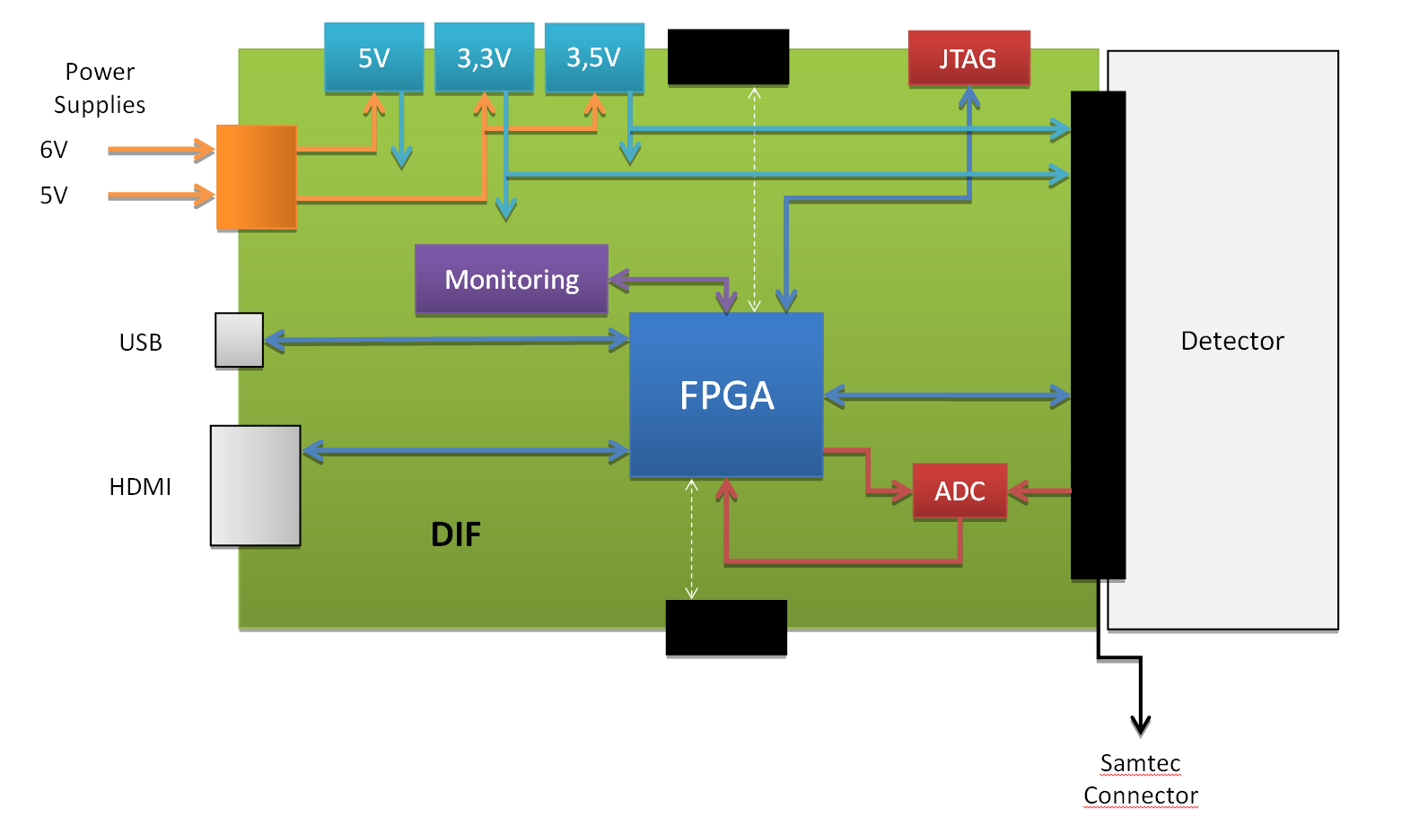
5.1.2 DIF interfaces
The DIF plays a central role in the DAQ system. It links the active layer to the external DAQ devices. This is done through the following interfaces:
-
•
Detector interface
A connector made by the Samtec Company is used to establish the connection between the DIF and the ASICs of the ASU. It has 80 pins allowing to transmit and receive the different signals. It allows also to power the ASU. -
•
Data Acquisition (DAQ) interfaces
The two interfaces linking the DIF to the DAQ are the following :
1-USB Protocol. The USB transmission system is used for data transmission from the DIF to the computer network and for receiving non synchronous commands (like the ASIC configuration one) from the computer network. It is used also for register control to read and write actions. To handle the USB communication protocol an FTDI chip is used.
2-HDMI Link. The HDMI transmission system is used for sending the clock and synchronous commands to the ASIC. It allows in Test Beam configuration to provide the Trigger and Spill444Spill signal is used to drive the ASU power pulsing. signals. It is also used to concentrate Busy and RAMfull signals from the DIF to the SDCC. Those 2 signals are mandatory for the synchronization of the whole system (see Section 5.2.4). The protocol used for the HDMI commands is a homemade protocol which includes a header, the command number and a checksum. Almost all the HDMI signals are real LVDS signals555Except pins 15 and 16 that can be used as LVDS signal but there are not twisted pairs..
5.1.3 DIF features
The FPGA on the DIF is the key element of the board. It controls everything on the board and performs all the features of the DIF. These features are summarized here after:
-
•
ASIC configurations
As mentioned before the SC parameters are used to configure the ASICs of the detector’s ASUs. Because of some spread in pedestal, gain and thresholds, each ASIC has a specific configuration. The SC parameters allow to homogenize all the ASIC responses. The command to transmit these parameters does not require synchronization; it is done by the USB transmission data system. When the command is started, the computer network sends the needed amount of data to configure all the ASICs. 872 bits are necessary to configure one HARDROC. There are 144 ASICs on each active layer unit. Therefore, more than 6 Mbits are sent to the prototype’s ASICs from the computer network. For each DIF, a 16 bit Cyclic Redundancy Check (CRC) is sent at the end of the SC parameters transmission to verify that it was correctly done. After receiving all the configuration parameters, the DIF forwards them to the ASIC through the Samtec connector. Since the configurations transmission is daisy chained, it is possible to return the configuration parameters from the ASICs to the DIF if the detector Printed Circuit Board (PCB) is routed for this purpose. In this case the DIF sends twice the configuration parameters to the ASICs so that the first configuration can be checked against any modification during the transmission process inferring that the 2nd configuration transmission is correct. -
•
Digital Readout
When the ASICs are configured, the data acquisition can be started and run according to one of the 2 following modes:
1-Trigger mode: In this mode the ASICs are active after the StartAcquisition signal. Upon the arrival of an external signal (for instance a coincidence signal from scintillator PhotoMultipliers system tagging the passage of a particle) a StopAcquisition signal is received by all the ASICs from the SDCC through the DIFs and followed by a StartReadout allowing to transmit the collected data to the DIFs. Since the ASICs are self-triggered, it may happen that the memory of one of them gets full before the arrival of the Trigger signal. In this case a RAMfull signal is produced by the ASIC and transmitted to the DIF which forwards it to the SDCC. A global signal is then sent from the SDCC to all the ASICs through their own DIF and their memories are reset before starting the acquisition process again.
Trigger mode is used generally when the time information of beam particles going through the detector cannot be extracted from the data only and one needs to discriminate the collected data due to the particles from those due to the noise. This is typically the case when dealing with a small number of chambers. This mode is also useful when particle identification signals (from e.g. Cherenkov detectors or a muon veto) enter the coincidence to enrich the purity of the event sample.
2-Triggerless mode: In this mode the ASICs are put into acquisition state at the start of a Spill signal (for instance the accelerator clock). When any of the ASICs has its memory full, it sends a RAMfull signal and, as for the Trigger mode, this signal is sent to the SDCC through the DIF and a global signal is sent back from the former to stop the acquisition process in all the ASICs, followed by a StartReadout signal to initiate the readout process .It is worthwhile to mention that in both modes when the acquisition process is stopped and the readout is started, a timestamp called Bunch Crossing IDentifier (BCID) , whose counter is synchronized with the ASIC’s one, is recorded by the DIF and included in the data stream. This allows an easier reconstruction and analysis of the data.
-
•
Power-pulsing (PP) mode
In the case of the future ILC, the active time corresponding to the beams Bunch Crossing (BC) is expected to last every . During the relatively long inactive period, the ASICs can be switched off in order to reduce the power consumption of the electronics and thus the heat dissipation in the calorimeters. Therefore a mode which consists in powering ON the ASICs during the BC and the subsequent readout and powering them OFF the rest of the time is extremely helpful. The same mode could be used during the test beam operations. In this configuration the power pulsing is synchronized with the accelerator clock by using the particle spill signal delivered in the control room. Nevertheless, in both the ILC and Test Beam conditions, when the chip is turned on, a certain programmable delay is applied before any detector signal can be recorded to the memory. This delay accounts for the stabilization of the various voltages and currents inside the chip. When the delay is too short the detector occupancy is dominated by noise. Measurements with oscilloscopes show that the typical delay to have the voltage stabilized is around (Figure 21). To keep a safety margin, the delay applied before detector signal can be recorded was set to . The PP mode could be used with either the Trigger or the Triggerless mode.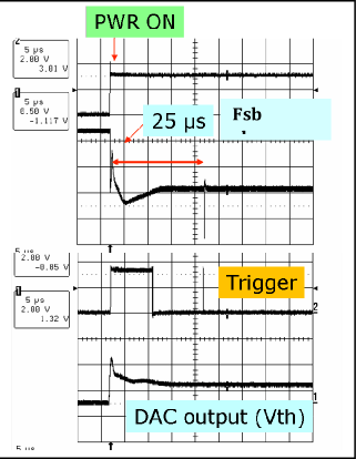
Figure 21: Voltage measured on various HARDROC lines showing the stabilization of a HARDROC threshold and FSB line voltages at a Power-On-Analog signal. An important point to mention here is that for the various modes, the readout of the ASICs is automatically performed at the end of the acquisition controlled by the SDCC. The DIF FPGA performs the readout of all ASICs under its control. The data are stored in the FPGA memory and sent with other information specific to the data format to the computer network through the USB link. While the FPGA performs the readout, it also generates a Busy signal which reaches the SDCC in order to avoid starting a new acquisition process, ending when all data are read out. Indeed, as soon as the last ASIC has sent his data, the busy signal is released and the DIF can accept again a new StartAcquisition command from the SDCC.
-
•
Data format
In order to facilitate the reconstruction and analysis of the data, additional information are added to the data stream according to a specified format. For every readout operation, the ASIC data are encapsulated by the DIF’s FPGA with a header, a trailer and the following information before they are sent to the computer:-
1.
DIF Trigger Counter (DTC): Coded in 32 bits, it counts the number of readouts. It is reset at the first acquisition of each run.
-
2.
Information Counter (IC) : Coded in 32 bits. Bits 23 to 0 are used to count the dead time. This occurs when ASICs are not acquiring. It is reset every acquisition. Bits 31 to 24 are used for BCID counter overflow. It is reset at the first acquisition of each run.
-
3.
Global Trigger Counter (GTC) : Coded in 32 bits. It counts the number of triggers received by the DIF when the Trigger mode is run and counts the number of readouts in the Triggerless mode. It is reset at the first acquisition of each run.
-
4.
Absolute BCID : Coded in 48 bits. It is incremented with the clock received from the SDCC. It is reset at the first acquisition of each run.
-
5.
BCID DIF : Coded in 24 bits. This is incremented with the clock coming from the SDCC and is synchronized with the ASIC BCID mentioned in section 4.1.
-
1.
5.2 Data Concentrator Card (DCC) and Synchronous DCC (SDCC)
5.2.1 (S)DCC architecture
The two boards have the same hardware. A (S)DCC board has a VME format. Each board has 9 HDMI connectors on one side and 1 HDMI, 1 USB and 2 lemo connectors on the other side. All the connectors are connected to an FPGA so that the FPGA can send the signal form one side to the other. The DCC differs from the SDCC by the FPGA firmware.
5.2.2 DCC interfaces
The two interfaces the DCC has are the following:
-
•
Synchronous Data Concentrator Card (SDCC) interface
The DCCs and the SDCC send each other information through the HDMI transmission system. The SDCC sends clock and commands to the DCCs and the DCC FAN IN sends the Busy and RAMfull signals from the DIFs to the SDCC. -
•
DIF interface
The DCC can be connected up to 9 DIFs. The DCC sends to all the DIFs the clock and the commands received from the SDCC in a synchronous way. Each DIF sends its Busy and RAMfull signals to the DCC.
5.2.3 SDCC interfaces
The SDCC has two kinds of interfaces. One is related to the DIF directly or through the DCC. The other one manages the link with the computer network.
-
•
Data Acquisition (DAQ) interface
The SDCC is connected either directly to up to 9 DIFs or to up to 9 DCCs to increase the number of DIFs connected to the DAQ. -
•
Computer network interface The SDCC is connected to the computer network to allow the user to control the DAQ.
The commands which need synchronization are sent from the PC to the SDCC through a USB transmission system, and then the SDCC sends the command to all the DIFs through the HDMI transmission system. These commands are sent with the clock, but they are serialized (SDCC) and deserialized (DIF) with a clock. The commands contain one header, the command number and a checksum. Some commands are only meant for the SDCC and are not forwarded to the DIF.
5.2.4 (S)DCC features
The DCC acts like a FAN OUT with the information coming from the SDCC and like a FAN IN with the information coming from the DIFs.
The SDCC is connecting the DAQ PC through its USB interface with the DIFs through 9 output HDMI connections. The main commands and signals controlled by the SDCC FPGA are summarized here after.
-
•
Trigger signal: In Trigger mode, the DAQ needs the trigger signal to stop the acquisition and start the readout of the detectors. A lemo connection is foreseen for this purpose on the SDCC board.
-
•
Spill signal: When the ASIC are power pulsed, the DAQ needs the duty cycle or the Spill signal from the accelerator. The signal should be active during the BC or the spill but also slightly a bit before (). This permits the DAQ to power ON the system when the spill signal is active and to power OFF the system when the spill is inactive. Another lemo connection is foreseen on that purpose on the SDCC board.
-
•
Busy and RAMfull signals: The Busy and RAMfull signals are used to maintain the synchronization and the automation of the different processes of the DAQ system. Both signals are sent from the DIFs and then concatenated in the DCCs up to the SDCC. Depending on the running mode, Trigger or Triggerless, the RAMfull signal can have different consequences. In the former it is followed by a reset of the ASIC memory while in the latter it initiates the readout phase. Concerning the Busy signal, it is active when the ASICs are being read out. While the Busy signal is active, a new start acquisition can not be sent. But as soon as the last Busy is unset from the DCCs connected to the SDCC, the SDCC sends a new StartAcquisition command to the different DIFs to launch a new acquisition. This is how the automation is done in the DAQ system.
6 The SDHCAL data acquisition software
The data acquisition software is split in three parts: the low level hardware access that hides effective hardware implementations, the configuration data base software handling devices description and SC parameters and finally the data collection and monitoring. All packages are written in C++ with interactive scripting in python. Low level and database C++ libraries are all parsed to python object with the Swig tool. It allows an interactive instantiation and debug of single code pieces.
6.1 The low level hardware access
6.1.1 USB readout
DIFs and SDCC FPGAs are interfaced with the same USB chip. As mentioned before this is an FTDI chip. The DIF is thus uniquely identified by its FTDI device identifier (id) stored in an EEPROM and access to a specific device id is done using either the proprietary library FTD2XX or the free version library libFTDI. A device driver library (UsbDeviceDriver) was develop ed to implement a set of low level access (read and write of registers) of the two boards.
6.1.2 DIF and SDCC readout
An upper layer software is dedicated to DIF configuration and DIF readout. The class called BasicUsbDataHandler aggregates a pointer to a UsbDeviceDriver and to a configuration buffer handling all DIF and SC parameters. Specific methods are used to implement the DIF configurations, the ASIC configurations and a single event readout to an internal buffer. Similarly, an SDCCDataHandler implements commands associated to the SDCC.
6.1.3 DIF Manager
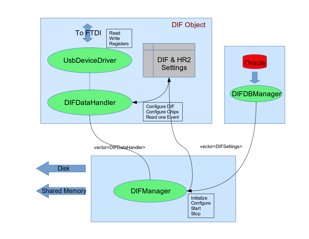
Eventually one DIF manager class per PC is responsible of the data taking of the DIFs through the USB connected to it. It handles the DIF and ASIC configuration parameters via an interface called DIFManager. This scans and detects all connected DIF, instantiates one DIFDataHandler class per detected device and distributes configuration parameters. When data taking starts, it starts a polling thread continuously reading events on all connected DIFs. Events can be directly dumped to disk in LCIO[7] format or transferred to the central data acquisition. Figure 22 summarizes this architecture.
6.2 The configuration database
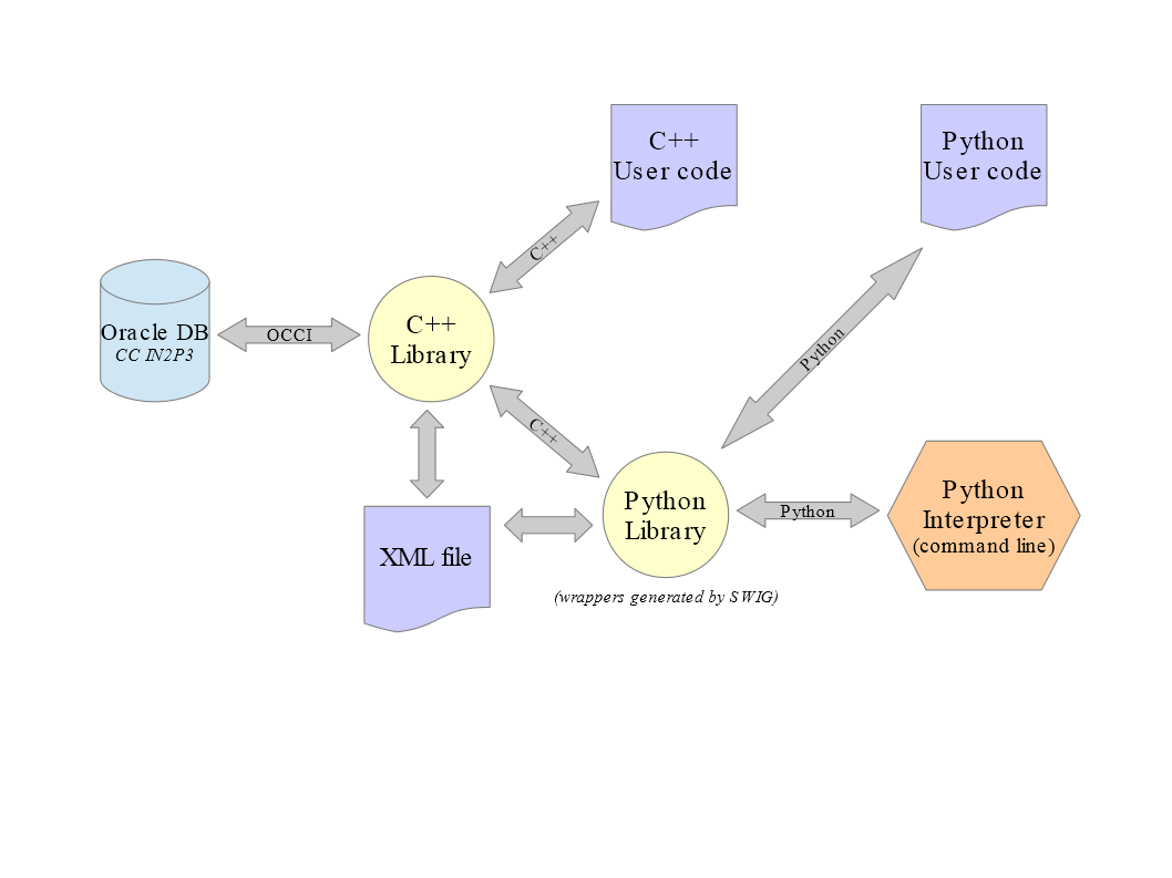
The configuration database gives the possibility to store and retrieve all parameters needed by the DAQ system. The database itself is hosted on an Oracle server at CC IN2P3 (Villeurbanne, France). To interface this SQL database with the DAQ software and to allow users to insert and query data without knowledge of SQL, a C++ library has been written. Part of the DAQ system being written in Python, we used Swig to generate a Python version of the C++ library. The system has been designed to easily allow the addition or modification of existing object parameters. It is built on 2 levels: the database itself and the C++ library.
6.2.1 Database model
The database model is conceived to deal with extendable number of ASICs. It can also handle different kinds of ASICs using different settings of parameters to take into account addition of other sub-detectors. In this model, each ASIC has a unique entry in the ASIC table, containing its type. The actual configuration parameters are contained in 2 tables: the first is ASIC_CONFIG for the parameters common to all ASIC types and the second <ASIC_TYPE>_CONFIG for the parameters specific to a given type. For instance the configuration parameters for a HARDROC ASIC will be stored in the ASIC_CONFIG table for the common part and in the HR2_CONFIG table for the HARDROC specific parameters666Here label HR2 is to indicate that we are using the version 2 of the HARDROC ASIC.. As a consequence, supporting a new type of ASIC requires only to create a new table containing the specific configuration parameters. When downloading the parameters, the system will automatically choose the accurate tables associated to the type of the concerned ASIC.
6.2.2 C++ Library
All accesses to the database are done through the C++ library. There are no mention of the actual configuration parameters in the library: all names of parameters are retrieved from the database itself at runtime. The methods used to set or to get parameters value in the application (API) use the parameters name as an argument (ex: setInt("B0",5) and getInt("B0") ) to respectively set and retrieve the integer value of the B0 parameter). As a consequence, there is no need to modify the C++ library when modifying parameters or adding new types of objects. This will be done dynamically from the database itself. Each stored configuration is associated with a version number having the form "MajorID.MinorID". A configuration with version number 1.0 will contain all the parameters for all the DAQ objects, whereas a configuration with version number 1.X will only contain the modifications from version 1.X-1. This allows a reduction in the amount of data to transfer and to store.
6.2.3 Tools
The C++ library gives a high level access to the database, providing the possibility to manipulate the concepts of ASIC, DIF or Configuration without any SQL knowledge. It allows to create/modify/upload or download a complete setup defined as follows:
-
1.
Setup: a set of "states" (one per sub-detector).
-
2.
State: a coherent set of "configurations".
-
3.
Configuration: a list of basic objects.
-
4.
Basic object: a unique object with all its parameters (ASIC, DIF, DCC, …) .
Figure 23 illustrates the structure of such a setup.

In the case of the SDHCAL prototype with 50 active layers, a typical setup contains a single state with 150 DIFs, each having 48 ASICs connected. This corresponds to roughly 550 000 parameters. The download of such a setup takes around 5-7 seconds. In addition, the library allows to store information about a run (time, date, type, XDAQ configuration[8], setup used, …). Using Swig, a Python version of the C++ library is provided. It is in fact a collection of python wrappers to the C++ functions. It gives the possibility to access the database from Python scripts and allows the usage of the python interpreter as a command line tool to manage configurations. Finally, configuration setups can be imported/exported to/from the database using XML files. These files can be used to run an acquisition without access to the database which could be useful when access to database is interrupted for some reasons. Figure 24 summarizes the structure of database access using the different tools.
6.2.4 Data acquisition access
In order to minimize database access during data acquisition, a class called the DIFDBManager (Figure 22) is responsible of the download of all the DIF and ASIC configuration parameters of a given setup and to cache it for fast access. Data are stored in indexed maps that provide an instantaneous access to the data needed by one specific DIF. Each separate DIFManager instantiates one instance of DIFDBManager and uses it as a configuration cache.
6.3 The data collection
6.3.1 Local data acquisition and coherence
In order to keep the coherence of collected data, DIF readout outputs are synchronized using the absolute Bunch Crossing ID identifier defined in section 5.1.3. This is a 48 bits 5 MHz counter that is reset when the first acquisition starts after the DIFs are powered on. Data from different DIFs may be read out at different times but will have the same absolute BCID for a given Trigger (or RAMull) signal. The logical way to keep synchronicity is to store in a BCID indexed map the buffers of all read DIFs but this requires to manage memory allocation, access and cleaning. Recent Linux kernels offer the possibility to use shared memory based file, ie, /dev/shm. This special file system is directly mapped in the system memory and data can be written, listed and read with extremely fast access. Each DIF data block is written as a single file named Event_BCID_DIFID in /dev/shm and an empty file /dev/shm/closed/Event_BCID_DIFID is created once the event file is closed by the DIFManager. Standard C functions are used to list events available, to read, write and delete data. This method allows to separate the process reading data from those making data collection, writing, debugging and monitoring in a single computer without special protocol or API to be used.
6.3.2 Global data acquisition with XDAQ
Whenever several computers are involved in the data taking, a communication framework is needed. We choose to use the CMS data acquisition XDAQ framework [8]. It provides:
-
•
A communication with both binary and XML messages.
-
•
An XML description of the computer and software architecture.
-
•
A web-server implementation of all data acquisition applications.
-
•
A scalable Event builder.
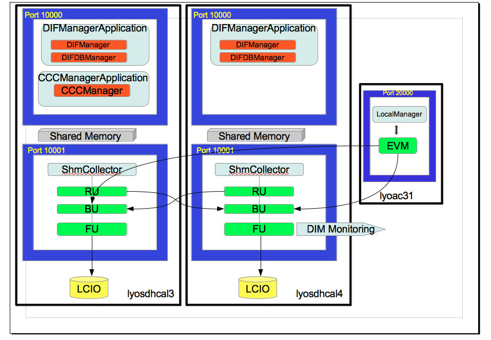
Each PC handling DIFs hold a DIF manager XDAQ application obeying to a message driven state machine responsible for initialization ( USB scan (section 6.1.3) and DB download), configuration (DIF and ASIC settings) and running (DIF readout and /dev/shm storage). A second application (ShmCollector) scans the shared memory and pushes completed events to the local event builder application (Readout Unit). The main advantage of the CMS event builder is the scalability. It is possible to add any number of collecting applications (Builder Unit) that will merge data from all Readout Units for a given trigger. Those Builder Units distribute merged events to any analysis and data writing application (Filter Unit) declared to them. In the SDHCAL case, the computing capability is handled by the PC reading the DIFs, so one Readout Unit, one Builder Unit and one Filter Unit application are created on each PC as described on Figure 25 and each Filter Unit writes the associated data in a separate stream.
The whole system is controlled by the Event Manager (EVM). It collects the list of free slots on all Builder Units and generates an associated number of tokens sent to the LocalManager. This last application is the trigger master of the system. As long as it has free tokens, it sends software trigger to the Event Manager that distributes them to one of the free Builder Units. Once an event is built, a new token is sent to the LocalManager. Any trigger strategy (pause for calibration, software back pressure…) has to be implemented in the LocalManager.
6.4 Run Control
The run control developed in CMS could have been used here but its deployment for small Beam Test experiments is heavy. Alternatively a set of python script was developed to create XML description of application content of each computer (DIFManager, CCCManager (controls SDCC), Database). Then a second set of python scripts uses the web capabilities of the XDAQ application and sends SOAP or XMLRPC messages to each server to trigger the final state machine of the applications. The global state machine (Initialise, Configure, Enable, Stop, Halt, Destroy) is coded in these python scripts. Eventually a Qt based graphical user interface is provided, using PyQt [9] framework to bind python methods to graphic widgets.
6.5 Online Monitoring
The online monitoring is a two steps process:
-
•
A XDAQ application LCIOAnalyzer runs in a standalone mode, waiting for events to be sent by each of the Filter Unit in a sampling mode ( 1%). Events collected are stored and a separated thread analyzes the events using the ILC analysis program MARLIN [10] allowing any developer to deploy its own analysis code. The ROOT[11] histograms are booked in memory by a singleton class that keeps a map of all histograms booked by any of the analysis modules.
-
•
The LCIOanalyzer answers SOAP commands to return the list of histograms names and an XML encoding of the requested histograms. Clients, using XMLRPC or SOAP request in python, can access the XML answers remotely and using PyROOT [12] can recover requested ROOT histograms and display them. Once again a PyQt graphical interface is provided to ease the user access.
This distribution of ROOT histograms is useful since users are able to manipulate the histograms (zoom, fit…) and not only their image. This distribution is limited however to a relatively small number of clients ( 10).
6.6 Acquisition system performance
The readout mode we used in Test Beam configuration is the ILC mode. The ASIC acquisition is started via a command from the SDCC, each chip acquires a 20 bytes frame synchronized with the 5 MHz clock whenever one of the 64 channels fired a threshold. Once an ASIC reaches 127 frames buffered, it triggers a RAMfull signal to the SDCC which sends back a StopAcquisition to all ASICs and a StartReadout command to empty their buffer and send data on the USB bus. Once all ASICs are read a new StartAcquisition is triggered for the next event. In a pure ILC mode (1 ms data taking , 200 ms inter crossing) the StopAcquisition is forced at the end of the crossing.
With an optimal noise of 1 Hz/pad, each ASIC is able to acquire frame during 2 s. The average size of data read by a DIF is then kbytes. Those 60 kbytes/s are read using a serial line at 5 MHz on the ASU and a 10 Mbit/s USB1 bus. So we expect in this best case a dead time of 180 ms due to the ASU readout and 90 ms due to the USB one. The slow control commands handling by the DIF and SDCC is limited to less than 20 s and can be neglected. That leads to an average availability of 88 %, that can be increased to 92 % if an USB2 readout is used.
Unfortunately this readout mode is driven by the most noisy ASIC in the SDHCAL. Local variation of the gap, of the painting resistivity or of the temperature may lead to hot spots where the noise can reach hundreds of Hz. A few ASICs ( 2 %) located on the edge of very few chambers reach up to 4 kHz. The reason behind such behavior was found to be a slightly reduced frame height leading to a locally increased electric field. Still, with such high noisy spot the readout rate could reach 30 Hz and the availability decreases to 8 %. Masking the most noisy ones and using USB2 protocol a data taking availability of 20 % was achieved during Beam Tests.
One should notice that in pure ILC mode (1ms crossing, 200 ms off), the tiny acquisition time guaranties full availability of the detector despite those local high-noise ASICs.
6.7 Recent developments
One critical point in the previous architecture is the number of USB devices that are to be read simultaneously. Moreover, since USB bus was originally foreseen as a debug channel the chip only support USB1 (10 Mbit/s) protocol. Reading 150 USB devices on a single PC is then extremely slow and we split it on 4 different PCs with up to 7 buses (42 devices) read in parallel.
With new pocket size, ARM based PC, availability like the rapsberry Pi [13], we were able to bring low cost (30 $) and low consumption (< 3 W) computers and buses near the detector. We developed a homemade USB hub plugged on the raspberry Pi with 12 USB channels available on one bus and connect it to 4 chambers. Thirteen raspberrys are used to read the SDHCAL. Since XDAQ software is not yet available on ARM architecture, the central DAQ is rewritten using the lighter DIM [14] acquisition middleware.
In parallel the USB1 chips on the DIF was replaced with a USB2 equivalent chip. New buses speed and lower number of devices on each bus improves performance by 50 %.
7 The SDHCAL prototype mechanical structure
7.1 The Design
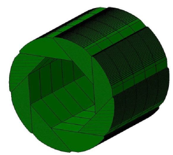
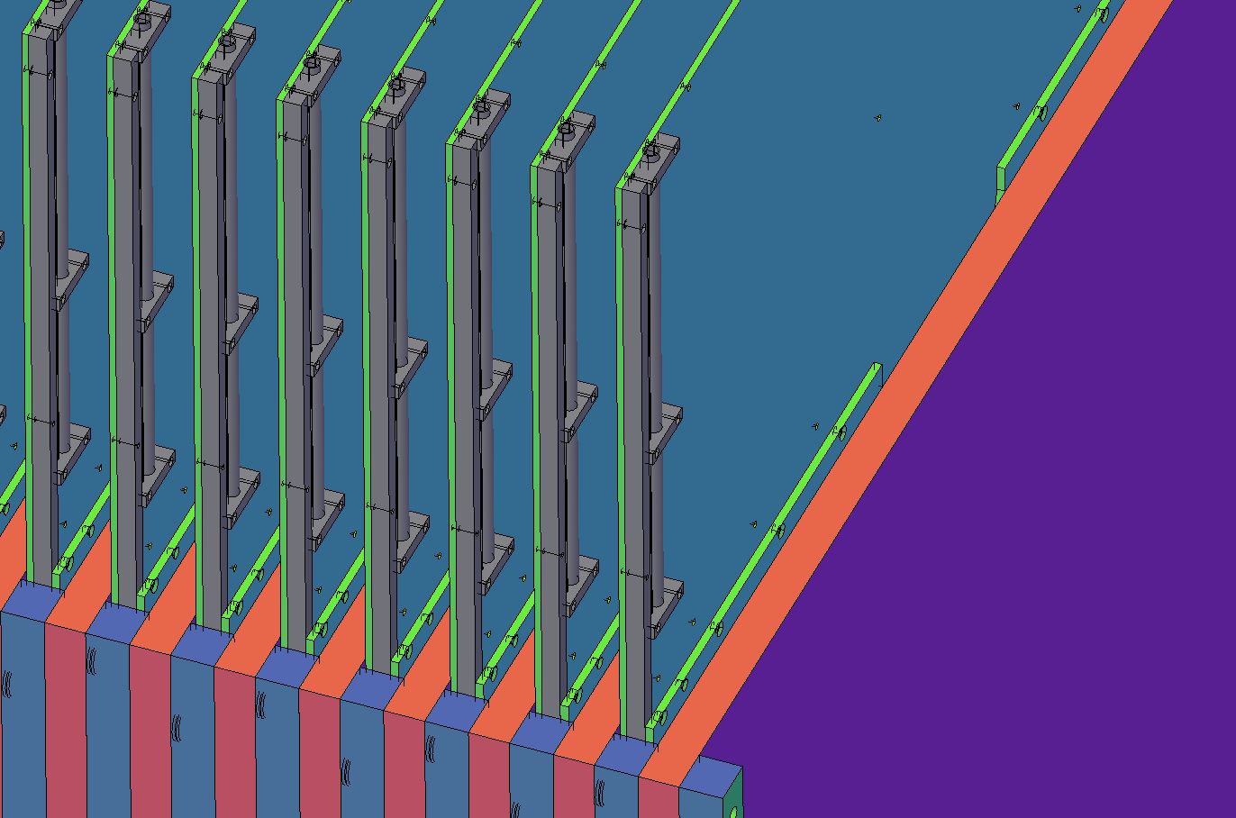
The mechanical structure of the SDHCAL prototype was conceived as a demonstrator of the one we propose for the International Large Detector (ILD) [15]. Figure 26 left shows the design layout for the barrel part of the ILD SDHCAL. The design is self supporting and has been optimized to reduce cracks. The barrel consists of 5 wheels each made of 8 identical modules. Each module is made of 48 stainless steel absorber plates interleaved with detector cassettes of different sizes as shown in Figure 26 right. A simpler geometry has been adopted for the prototype: a cubic design with all plates and detectors having the same dimensions of .
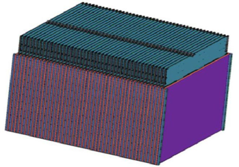
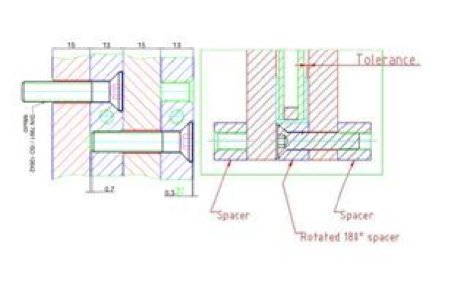
Figure 27 (left) shows the prototype design. It consists in a mechanical structure, made of the absorber plates, that hosts the detector cassettes. The design allows an easy insertion and further extraction of the cassettes.
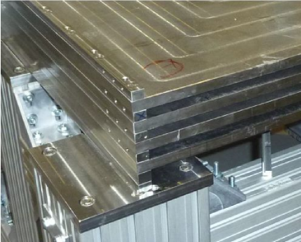
The mechanical structure is made of 51 stainless steel plates assembled together using lateral spacers fixed to the absorbers through staggered bolts as can be seen in Figure 27 (center and right). The dead spaces have been minimized as much as possible taking into account the mechanical tolerances (lateral dimensions and planarity) of absorbers and cassettes, to ensure a safe insertion/extraction of the cassette. The plate dimensions are . The thickness tolerance is and a surface planarity below 500 microns was required. The spacers are thick with accuracy. The excellent accuracy of plate planarity and spacer thickness allowed reducing the tolerances needed for the safe insertion of the detectors. This is important to minimize the dead spaces and reduce the longitudinal size in view of a future real detector.
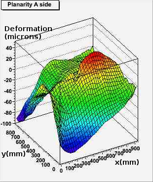
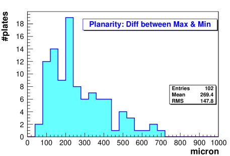
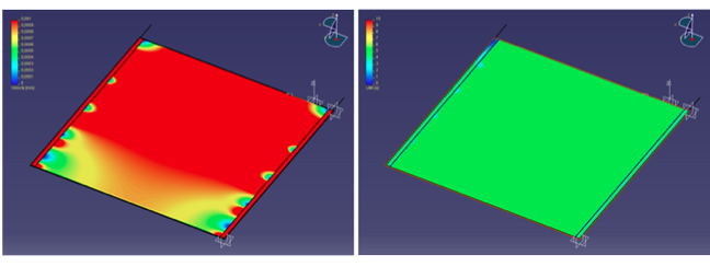
The thickness and flatness of the plates used for the prototype have been verified using a laser interferometer system in order to certify they were inside the tolerances. Figure 28 (left) shows, as an example, the planarity distribution for one face of one of the plates. For this particular plate the maximum deviation from planarity is lower than . For most plates the maximum does not exceed the required . Figure 28 (right) shows the maximum deviations from planarity for all plates.
7.2 Assembly of the mechanical structure
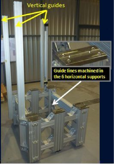
For the assembly of the mechanical structure a special table has been designed and built (Figure 29 left). This table must support a weight of about 6 tons. The table has vertical guides attached to the table and horizontal guide lines machined in 6 supports for the positioning of the first spacers. Plates and spacers are piled up and screwed together. Figure 29 right shows a detail of one corner of the assembly of the first plates.
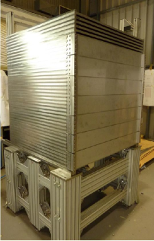
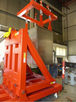
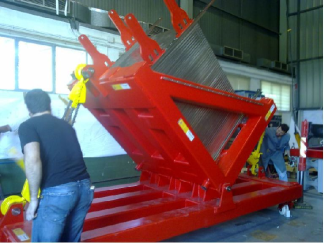
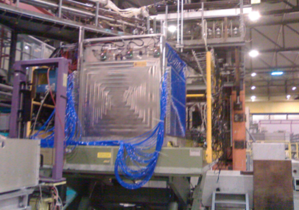
Figure 30 left shows a picture of the mechanical structure almost finished. The bottom of the structure is closed with stainless steel plates of thickness, fixed with bolts to the structure. Once the structure was completed it was placed (Figure 30 center) in a rotation tool specially designed and it was rotated (Figure 30 right) to vertical position. This rotation tool serves not only to rotate the mechanical structure but also the full prototype once it is equipped with the detector electronics and cables. This could be useful to change the orientation to test it in beam tests (vertical) and cosmic rays (horizontal).
The structure deformation has been checked during the assembly and after rotation using a laser interferometer and a 3D articulated arm. The total length of the prototype was larger than the nominal, and the parallelism between the first and the last absorber plate was . In fact some extra length was expected due to the cumulation of the extra thickness in the spacers and plates, because, in order to guarantee the space needed between the absorber plates for the GRPC insertion, the thickness tolerance of the spacers was , and, in addition, the thickness of the absorber plates has the same tolerance. The vertical misalignment between plates was below . This misalignment was due to an unexpected error during the manipulation of the structure that introduced some deformation, but, nevertheless, it does not interfere with the GRPC insertion. During the rotation the induced deformation of the structure was below , this guarantees the possibility to rotate the structure with the GRPC installed inside without introducing forces that could damage the detectors.
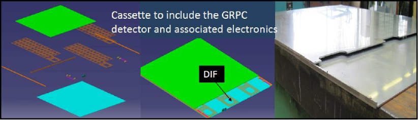
7.3 The Detector mechanical structure: the cassette
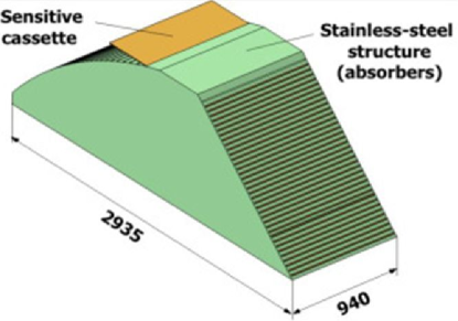
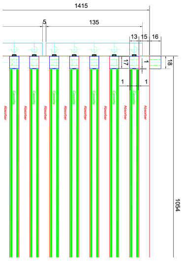
The GRPC detector together with its associated electronics is hosted into a special cassette which protects the chamber, ensures a good contact of the readout board with the anode and simplifies the handling of the detector. The cassette (Figure 32) is a box made of 2 stainless steel plates thick and stainless steel spacers machined with high precision closing the structure. One of the two plates is larger than the other. It allows fixing the three DIFs and the detector cables and connectors (HV, LV, signal cables). A polycarbonate spacer, cut with a water jet, is used as support of the electronics; it fills the gap between the HARDROC ASIC improving the rigidity of the detector. A Mylar foil ( thick) isolates the detector from the box. The total width is , 6 of them correspond to the GRPC and electronics, and the rest is absorber. Figure 31 shows a schematic of the cassettes position inside the mechanical structure as well as an artist view of it.
7.4 Integration of the GRPC in the structure
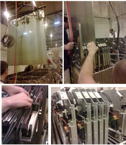
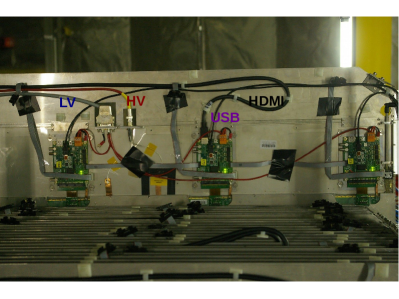
A total of 48 cassettes equipped with detectors and their embedded electronics have been built and inserted in the mechanical structure. The insertion has been made from the top with the help of a small crane as it is illustrated in Figure 33. Vertical insertion minimizes the deformation of the cassettes making easier the procedure. Each cassette is connected to 8 cables. Three of them correspond to the USB readout connections, three others correspond to the HDMI connections, and the others carry the high and low voltage. The gas is distributed individually to each GRPC. Figure 33 shows a detail of the external cabling distribution in the cassettes. Figure 34 shows the final prototype during one of the beam tests.
After the final assembly several cassettes have been extracted for reparation of some electronic connectors, the operation was done always smoothly without problems.
8 Event building
When running in the Triggerless mode in beam tests (See Section 5.1.3), each ASIC auto-triggers and stores the information according to the scheme described in section 4.1. In this scenario, the acquisition system reads the full detectors when the memory of at least one ASIC is full. The collected data thus include not only the information about the incoming particles (pions, muons or cosmic rays …) but also the intrinsic noise of the detector. The average duration of one acquisition window was found to be typically of . The time of each fired channel (called hit here after) with reference to the start of the acquisition is recorded by the BCID counter (See Section 5.1.3) increasing by a step of .
8.1 Preliminary data format
The raw data are then stored in LCIO format[7] by the acquisition system. Each acquisition window is stored in a preliminary LCIO file as an LCEvent. The LCEvent contains a collection of LCGenericObject containing the raw DIF data blocks (see Section 6.3). The first data processing is to convert these data blocks into a collection of hits including Bunch Crossing ID (BCID), the ChannelID, AsicID and DifID.
8.2 The algorithm
The physical event candidates are built from hits collection using a time clustering method. First, the time slot (i.e. BCID) with at least hits are selected. For each of these selected time slots, hits belonging to the adjacent time slots in a window of are combined to build a physical event. Care was taken to ensure that no hit belongs to two different events. Indeed if after the time clustering procedure, two events are found to have a common time slot, the hits of the common slot are assigned to the first event777This scenario was never observed during several beam tests at CERN. This is due to the reduced beam intensity used during beam tests given the limited GRPC rate capability.. The information related to the coordinates of the hits, determined from the location of the fired pad and the related active plate are then saved together with the threshold reached (either 1, 2 or 3).
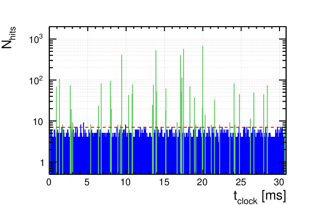
For the SDHCAL prototype the value is chosen as minimum of hits required to build an event (Figure 35). This allows the rejection of intrinsic noise while eliminating a negligible fraction of hadronic showers produced by pions of energy larger than .
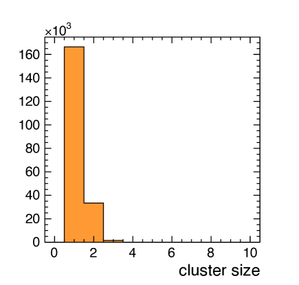
The width of the time window can be determined from the time cluster size built around (time slot with ) and including adjacent time slots in which at least one hit is recorded. As shown in Figure 36, hadron interaction events are contained essentially in two time slots of . In our event building a width of was chosen. Extending this width to 4 or 5 time slots was found to be of no consequence on our study.888The increase of number of hits associated to such events in these cases, was found to be compatible with an increase due to the noise which is less than one hit on average.
8.3 Geometry building
The information provided by the acquisition chain about the hit contains identification numbers (DifID, AsicID, ChannelID) and the position of the DifID in the layer and the detector. The relative position of pads in the ASIC, and the position of ASICs in the DIF are known from the hardware configuration. These information combined with the relative positions of the DIF and chambers in the calorimeter allow the reconstruction of the hit coordinates.
8.4 Coherent noise effects and mitigation
Some of the collected events in the prototype are not related to particles interaction. They are characterized by the recurrence of many hits belonging to the same electronic slab or to the whole electronic layer (made of three slabs), as shown in the Figure 39. The reason behind the occurrence of such events was identified to be the prototype’s grounding quality. The frequency of this coherent noise was indeed reduced by improving the grounding of the whole detector. This was achieved by connecting the cassettes to each other using metallic connectors adapted to the cassette geometry. In addition, for each active layer of the prototype the grounding of the electronic board was connected to that of the acquisition board and both of them were then connected to the cassette grounding. The grounding of the HV module was also connected to that of the LV grounding at the power supplies level. Applying this scheme improved the grounding significantly but did not eliminate all the related problems and events related to coherent noise, although very rare, are still present. It is clear that a global grounding of the detector is to be necessarily taken into account at early stages of the design to minimize loops and ensure an effective and reliable grounding of all the system.
8.5 The C++ package
The introduced event-builder was implemented in a C++ framework called Trivent. The core algorithm is implemented as a Marlin[10] processor. It takes as input an LCIO file with a collection of LCGenericObejcts containing all the information saved by the detector, where a LCEvent corresponds to a RAMfull. A configuration file in xml format containing the relative position of DIF in the detector is required.
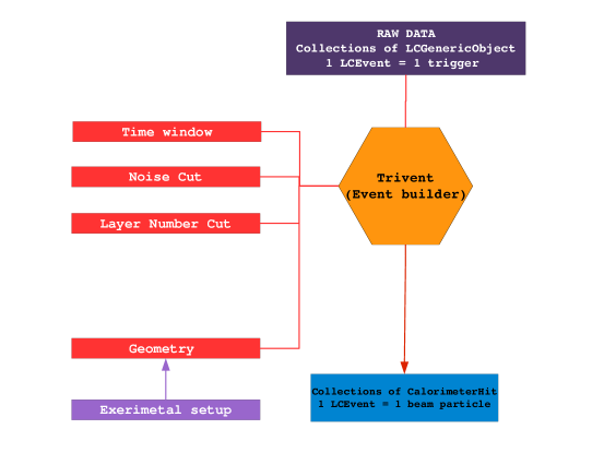
The running of the program is done by supplying a steering file containing the processor parameters (cut-list, file paths, etc). Trivent provides, after running, a LCIO file containing CalorimeterHit collections, in which each LCEvent corresponds to a physical event candidate. The Figure 37 summarizes the Trivent working flow.
8.6 Data quality control
During the data taking of the beam test periods, several controls have been done to check the validity of the saved data.
8.6.1 Online monitoring
First, an online monitoring reads the data stream from the DAQ and makes a fast analysis in order to estimate the chip occupancy (chip noise) and the detection efficiency of each chamber. The online monitoring constitutes an important step in the data taking, since noisy channels can be isolated and masked at very-frond-end electronic level during data taking.
8.6.2 Offline monitoring
Using the event-builder previously introduced, an offline monitoring is performed. It is focused on the measurement of noise, and the performance of chambers and their stability over the time.
8.6.3 Noise estimation
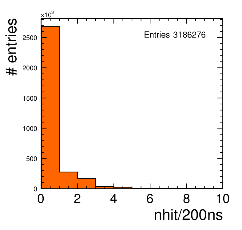
Two kinds of noise can be distinguished: intrinsic and coherent noises. Intrinsic noise is made of hits not related to a particle-interaction event (Figure 35). It is essentially due to the gain fluctuation in GRPCs in some zones like the ones around the spacers. Its intensity is a function of the temperature and the polarisation high voltage values. Pads whose intrinsic noise frequency was found to exceed 100 Hz were identified. Their number was found to be around few per mille.
The Figure 38 shows a typical distribution of this noise in units of the DAQ clock tick with an average of . This measurement gives an estimation of the contamination of noisy hits along physics events and shows that the GRPCs are almost noise-free.
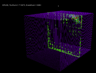
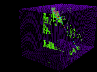
The coherent noise events are related to grounding problems as previously mentioned. They are easily identified and removed since the hits of such events are concentrated in one or two layers. The ratio of such common-mode noise events was found to be of the total events. Further selections, based on more sophisticated variables, can be used to avoid the events piled-up with coherent noise.
8.7 SDHCAL data quality
The high granular calorimeters equipped with digital (semi-digital) readout can be characterized by the measurement of the detection efficiency and pad multiplicity. These two quantities condensate the intrinsic properties of the used sensor. They are needed for the monitoring and the calibration of the detector and are indispensable for a proper modeling in the simulation of the prototype (and any large detector). The reconstruction of the tracks left by the muons in the calorimeters, thanks to its tracking capability, allows the measurement of these quantities.
8.7.1 Track reconstruction
Only events with a total number of hits less than are considered for the further study999This number is chosen from the assumption that in the extreme case, a muons track can induce 4 fired pads in each of the plates, which corresponds to hits in total.. Events with more hits are typical of interacting particle showers.
8.7.1.1 Neighbour clustering
All hits in a given layer are clustered using a nearest-neighbour clustering algorithm. It consists in merging in each GRPC plate the hits sharing a common edge (Figure 40). The position of the cluster is determined as the unweighted average in the two directions and of the position of the centers of the fired pads. The errors on the position and are calculated as and spread divided by (assuming a uniform distribution ranges in ).

8.7.1.2 Clusters cleaning
A removal of the farther clusters using a distance between a cluster () and the event cluster set () is applied to the cluster set. This distance is defined by
| (1) |
were is the euclidean distance between two clusters in the GRPC plane. The clusters farther than are then dropped. Event having at least one remaining cluster with are skipped, to exclude any possible hard muon interaction in the calorimeter.
8.7.1.3 Track reconstruction
Tracks are reconstructed by performing minimisation. The reduced of the fits is calculated 101010z-axis is perpendicular to the plates, x-axis and y- axis are respectively horizontal and vertical. as
| (2) |
where the sums run over all tracking clusters and
| (3) |
define a parametric equation of the straight line in the space with four parameters (). The errors and refer to the standard spread of each cluster defined previously.
The minimisation is performed using the MINUIT package [16] implemented in ROOT framework [11]. One example of muon event is shown in Figure 41 representing a cosmic ray muon.
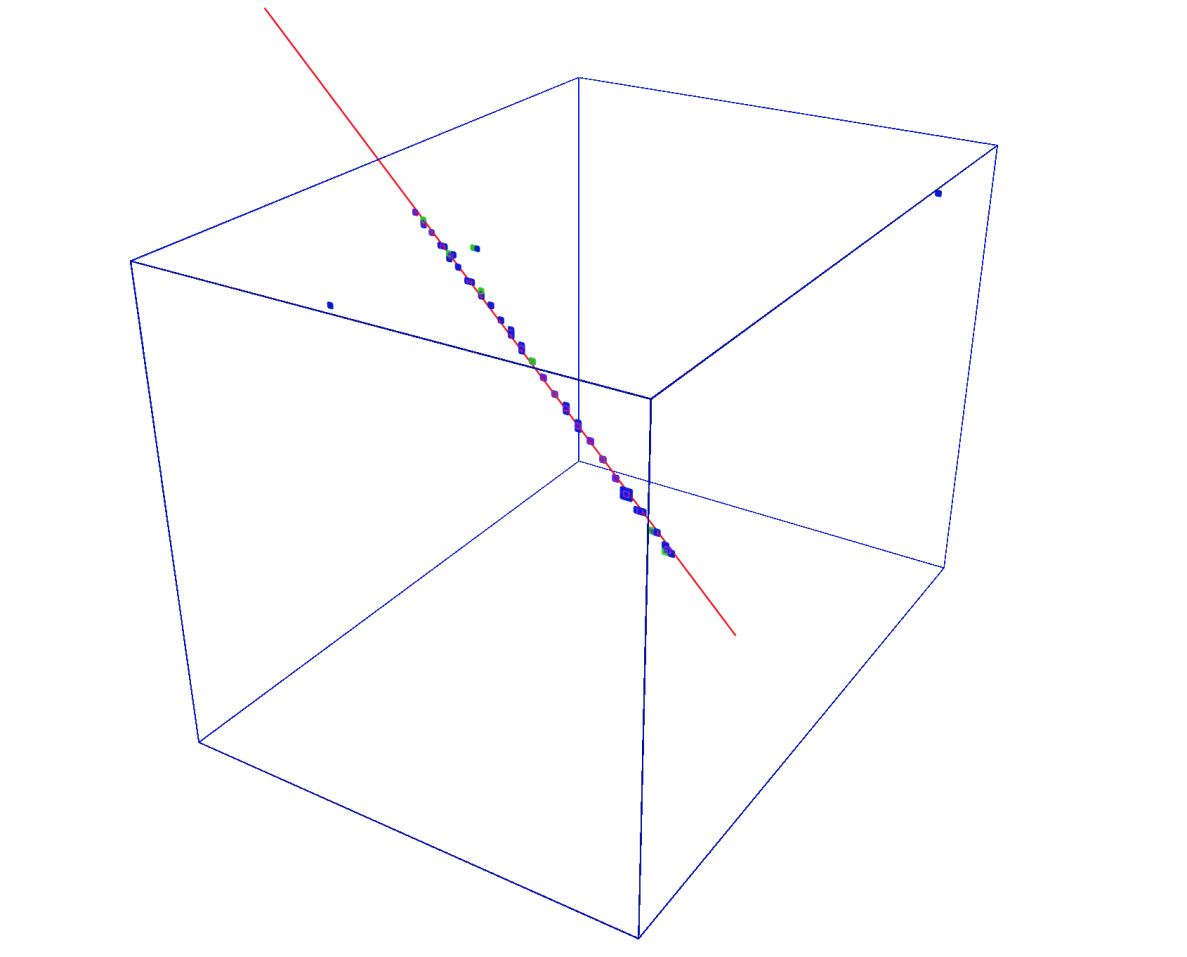
In order to estimate the performance of the GRPC, only tracks satisfying are considered for the further studies.
8.7.2 Efficiency and multiplicity
The efficiency of given layer is defined as the probability to find at least 1 hit within of the reconstructed track. The considered layer "" is removed from the track reconstruction to prevent any bias on the efficiency calculation. The multiplicity is defined as the mean number of hits matched on layer within of the track intercept for tracks with at least one hit matched. The Figure 42(a) and Figure 42(b) shows the efficiency and multiplicity for each layer.
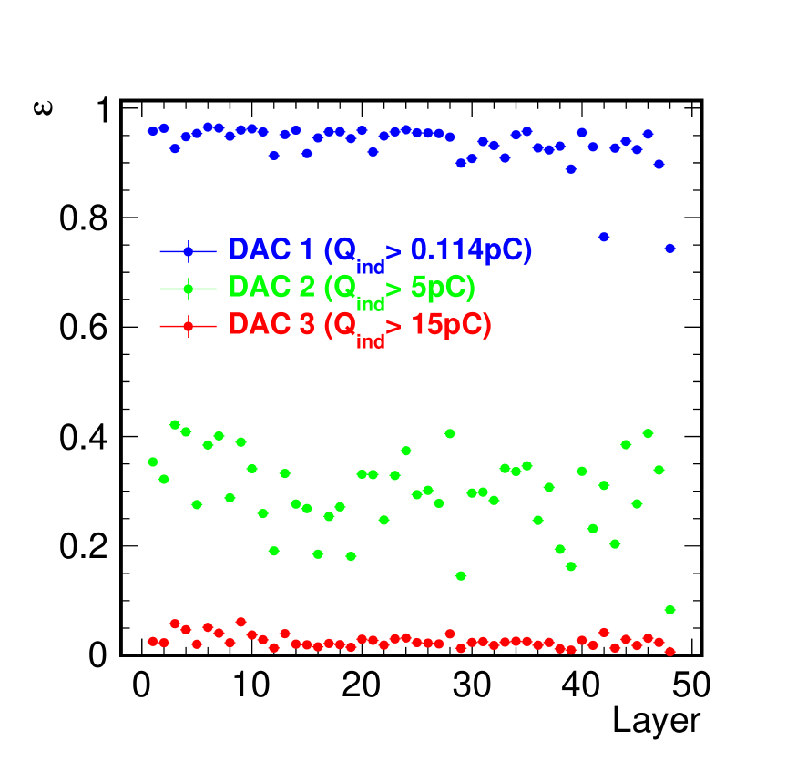
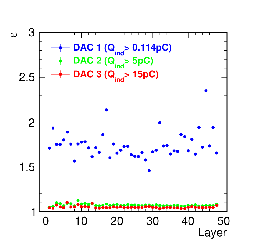
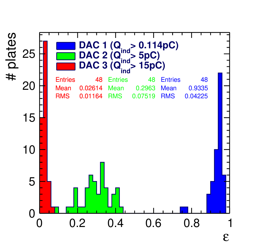
An efficiency of is observed over most of the chambers with an average multiplicity for the lowest threshold of about . The dispersion is essentially due to the fact that no gain correction is applied to the readout channels. However using clusters rather than hits in energy resolution is expected to reduce the effect of such dispersion.
9 Technical performance
To validate the SDHCAL performance, the prototype was operated with the power-pulsing mode during a beam test at the CERN SPS H2 beam line. The SPS duty cycle structure consisting of one spill with 9s time duration occurring every 45s was used. The prototype power consumption was measured during the spill when the electronic analog part is switched on but also in-between the spills when this is switched off. During the spill a total consumption of was recorded. Of this, only were consumed by the 6912 ASICs of the prototype. This consumption is equivalent to about per channel if the ILC duty cycle comes to be applied. The result is in a rather good agreement with the value of measured using a dedicated test board on witch one HARDROC ASIC was operated in the power-pulsing mode using the foreseen ILC duty cycle scheme. The remaining part is consumed in the buffers located on the ASUs inside the cassettes () and in the DIFs’s components (). In the DIFs are consumed by the regulators used to reduce the voltage from to and could be eliminated in future versions of the DIF and are consumed in the DIFs themselves 111111This consumption could be reduced in a future version by using low-power digital parts.. These are not affected by the power-pulsing mode and represent the essential of the prototype consumption during the time between the spills. The position of the DIFs outside the detectors prevents that the heating of the DIF components and more particularly that of the regulators to influence directly the active layer performance. Although the heat produced by the DIFs was found to have negligible effect in the case of the SDHCAL prototype, it should be evacuated using adequate cooling system in future experiments where the SDHCAL is expected to be placed inside the magnet.
For what concerns the power dissipation due to the ASICs and the few buffers of the ASUs121212One buffer per ASU. the contact of the ASICs with the stainless steel cover of the cassette allows to dissipate the heat through the absorber. The simple lateral cooling system described in the introduction is used to evacuate the absorber heat. The temperature stability of the prototype using such a system with the power-pulsing mode applied using the SPS duty cycle was checked by recording the temperature of three probes positioned inside three different cassettes. One of these three cassettes was chosen to be in the first part of the prototype, the second in the middle and the third in the rear. The probes were fixed in the middle of the 1m2 electronic board between the ASICs. Figure 43 shows the evolution of the temperature measured by the three probes for several days. The day-to-day as well as day and night variation of the ambiant temperature are observed but there is no clear increase due to the prototype running operation. Another important observable which reveals the stability of the active layers during the running operation is the stability of the current of each detector. This current which is due in part 131313 The GRPC current includes also the contribution of the detector leakage current. to the gas gain inside the detector and which increases with temperature was monitored and found to be stable during the data taking.
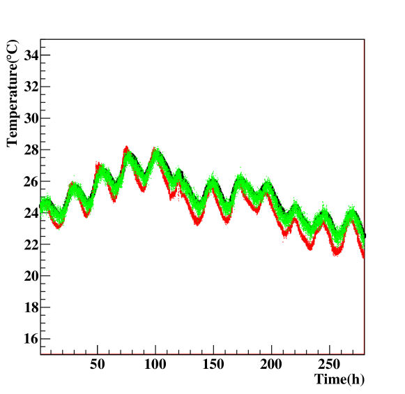
No attempt was made to switch off the lateral cooling system while operating the prototype using the power-pulsing mode according to the SPS duty cycle. Indeed, a thermal study based on the simulation of the ASICs power dissipation in the prototype was performed without the lateral cooling system. A relative increase of 4.6 ∘C was found in the central part of the prototype with respect to the ambient temperature. This increase of temperature would lead to more noise in the central part of the detector and thus a degradation of the prototype data quality.
Although one expects that running the SDHCAL prototype with the power-pulsing mode using the future ILC duty cycle will produce much less heating, the need of an appropriate cooling system should be assessed taking into account the geometry of the future SDHCAL and the constraint imposed by the global detector structure.
The stability of the prototype mechanical structure was also checked. Muons beam as well as cosmic rays were used to study the deformation of the structure by measuring the relative displacement of each layer with respect to the others. To perform this, tracks built using the clusters left by the passage of muons in the other layers as explained in the previous section were used. The residuals in both the horizontal (x-axis) and the vertical (y-axis) directions in each layer were obtained by comparing the expected impact parameter of the track and the barycenter of the associated cluster if any cluster is found in the layer in question. Figure 44 shows the residuals and for all the layers. The residuals in the horizontal direction seem in agreement with the lateral mechanical clearance between the cassettes and the mechanical structure. The residuals in the vertical direction indicate a slight bending of few millimeters in the middle. This can be explained by a displacement of the plates of the prototype due to a small incident that occurred during one of the first manipulations of the prototype as explained in 7.2.
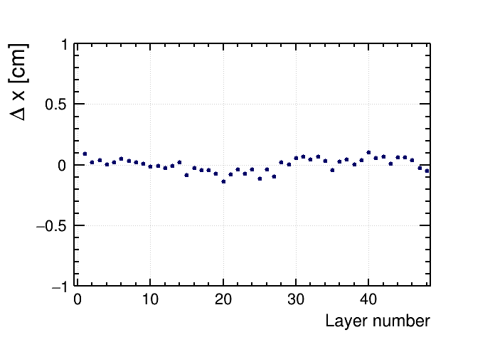
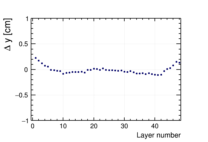
References
- [1] J Brient J-C and H Videau The Calorimetry at the future e+ e- linear collider eConf C 010630 E3047 arXiv:hep-ex/0202004 [hep-ex]
- [2] ALEPH Collaboration, D. Buskulic et al., Performance of the ALEPH detector at LEP, Nucl. Instrum. Meth. A360 (1995) 481?506.
- [3] M. Bedjidian et al.,, Performance of Glass Resistive Plate Chambers for a high granularity semi-digital calorimeter, JINST 6 (2011) P02001.
- [4] M. Bedjidian, J. C. Ianigro, R. Kieffer, I. Laktineh, N. Lumb and S. Vanzetto, Glass resistive plate chambers for a semi-digital HCAL, Nucl. Instrum. Meth. A 623 (2010) 120.
- [5] S. Callier et al., HARDROC1, readout chip of the Digital HAdronic CALorimeter of ILC, Nuclear Science Symposium Conference Record, 2007. NSS ’07. IEEE 3 (2007), 1851-1856.
- [6] S. Callier et al., ROC chips for imaging calorimetry at the International Linear Collider, JINST 9 (2014) C02022.
- [7] S. Aplin, J. Engels, F. Gaede, N. A. Graf, T. Johnson and J. McCormick, LCIO: A Persistency Framework and Event Data Model for HEP, SLAC-PUB-15296.
- [8] V. Brigljevic, G. Bruno, E. Cano, A. Csilling, S. Cittolin, D. Gigi, F. Glege and M. Gulmini et al., Using XDAQ in application scenarios of the CMS experiment, eConf C 0303241 (2003) MOGT008 [hep-ex/0305076].
- [9] \hrefhttp://www.riverbankcomputing.com/software/pyqt/introhttp://www.riverbankcomputing.com/software/pyqt/intro
- [10] F. Gaede, Marlin and LCCD: Software tools for the ILC, Nucl. Instrum. Meth. A 559 (2006) 177.
- [11] \hrefhttp://root.cern.ch/http://root.cern.ch/
- [12] \hrefhttps://root.cern.ch/drupal/content/pyroothttps://root.cern.ch/drupal/content/pyroot
- [13] \hrefhttp://www.raspberrypi.org/http://www.raspberrypi.org/
- [14] C. Gaspar and M. Donszelmann, "DIM: A distributed information management system for the DELPHI experiment at CERN", Proceedings of the 8th Conference on Real-Time Computer applications in Nuclear, Particle and Plasma Physics, Vancouver, Canada, June 1993.
- [15] T. Behnke, J. E. Brau, P. N. Burrows, J. Fuster, M. Peskin, M. Stanitzki, Y. Sugimoto and S. Yamada et al., The International Linear Collider Technical Design Report - Volume 4: Detectors, arXiv:1306.6329 [physics.ins-det].
- [16] F. James and M. Winkler, MINUIT User’s Guide.
10 Conclusion
We have conceived and built a technological prototype as a demonstrator of the Semi-Digital Hadronic CALorimeter for the future ILC experiments. The prototype has shown that a highly-granular calorimeter fulfilling the requirements of compactness and relatively low-power consumption HCAL with PFA capability is achievable by using simple but efficient and robust detectors such as GRPCs. Preliminary results with pion beam, to be published in future papers, show that such a new generation of calorimeters can also provide very good energy measurement in addition to an excellent tracking capability. Additional efforts are still needed to validate completely the SDHCAL concept to equip the detectors of the future different lepton collider experiments. These efforts have been already initiated. They focus on improving the mechanical structure by opting for more robust and less deforming welding techniques like those using electron beams. Attempts to build mechanical structures using these techniques are ongoing in collaboration with CERN services. The construction of larger GRPC detectors (up to 3m2) and adapting their gas distribution system to keep the same efficiency achieved in the case of 1m2 detectors are also ongoing. Finally the readout electronics is being improved by replacing the daisy chain protocol by the I2C one which allows to address the different ASICs individually eliminating thus the eventual problem of neutralizing a large portion of one detector electronics if one ASIC comes to die. Concerning this last point an updated version of the HARDROC ASIC has been already conceived and produced. The new version equipped with the I2C protocole and additional interesting features such as the zero suppression and an extended dynamic range is being tested. Preliminary results show that the new features are successful. New electronic and acquisition boards are also being developed to cope with the new features of the HARDROC while taking advantage of the recent progress achieved within LHC update research programmes.
11 acknowledgment
We would like to thank all who contributed to the construction of the prototype. We would like to acknowledge the support provided by the following funding agencies F.R.S.-FNRS, FWO(Belgium), CNRS and ANR(France), SEIDI and CPAN (Spain).