Electronic band gaps and transport properties in periodically alternating mono- and bi-layer graphene superlattices
Abstract
We investigate the electronic band structure and transport properties of periodically alternating mono- and bi-layer graphene superlattices (MBLG SLs). In such MBLG SLs, there exists a zero-averaged wave vector (zero-) gap that is insensitive to the lattice constant. This zero- gap can be controlled by changing both the ratio of the potential widths and the interlayer coupling coefficient of the bilayer graphene. We also show that there exist extra Dirac points; the conditions for these extra Dirac points are presented analytically. Lastly, we demonstrate that the electronic transport properties and the energy gap of the first two bands in MBLG SLs are tunable through adjustment of the interlayer coupling and the width ratio of the periodic mono- and bi-layer graphene.
Since it was first successfully fabricated in experiment approximately ten years ago Novoselov2004 , graphene has become an important research topic in condensed matter physics and material science. Indeed, because of its unique characteristics, graphene has the potential to take the place of Si-based semiconductors in future applications Novoselov2004 ; Novoselov2006 ; AHCastro2009 ; Ma2010 ; Peres2010 ; Bolotin2008 ; Novoselov2005 ; Purewal ; Lee2015 ; Gregersen2015 . In recent years, many important properties of graphene have been explored, such as chiral tunnelling Novoselov2006 , the giant carrier mobilities of this material Bolotin2008 , the unusual integer quantum Hall effect Novoselov2005 ; Purewal , and the edge-dependant spectra of graphene nanoribbons Brey2006a ; Nakada . In particular, for graphene-based superlattices (SLs), new Dirac points (DPs) and the zero-averaged wave vector (zero-) gap have been observed MBarb2010 ; LBrey2009 ; LGWang2010 ; TXMa2012 ; changan2013 . The electronic properties of monolayer graphene (MLG) and bilayer graphene (BLG) SLs of various sequences have been studied using the transfer matrix method Bai2010 ; LGWang2010 ; TXMa2012 ; changan2013 ; PLzhao2011 ; Gong2012 ; XXGuo2011 ; ZhRzh2012 . In addition, structures with biased potentials Michael2009 ; johan2007 and heterostructures johan2007 ; Giannazzo2012 ; Ando2010 ; Yu2014 have been investigated. However, few studies have discussed the properties of periodic mono- and bi-layer graphene (MBLG) SLs, in which the MLG is decoupled from the BLG.
In this paper, we study the electronic band gaps and transport properties of MBLG SLs. We demonstrate that a zero- gap and extra DPs exist under certain conditions. The zero- gap opens and closes periodically, while the number of extra DPs increases with increased lattice constant values. The relationship between the zero- gap and the interlayer coupling for MBLG SLs with periodic sequences is revealed. Furthermore, the effects of the average interlayer coupling , which is dependant on and the ratio of the MLG and BLG widths ( and , respectively), on the electronic band structures of MBLG SLs are explored. This provides a tunable method of controlling electronic conductance using MLG and BLG by varying the values (note that, for MLG, the interlayer coupling is zero).
We begin with the electronic structure of BLG with the energy and wave vector close to the point, such that the one-particle Hamiltonian for the BLG is given by Johan2006 ; Edward2006 ; Snyman2007 ; Michael2009 ; johan2007 ; Ando2010 ; Yu2014 ; MZarenia2012
| (1) |
Here, is the electrostatic potential applied on the material, which is constant within each potential barrier or well. Further, and are the momentum operators,where m/s is the Fermi velocity and indicates the interlayer coupling in the BLG regions. It should be noted that can be tuned by adjusting the interlayer distance Long2015 . The wave function is expressed by four-component pseudospinors . Note that, when , Eq. (1) reduces to the MLG case. As a result of the translation invariance in the direction, the wave function can be rewritten as , ,…,. By solving this eigenequation, the wave functions at any two positions and inside the th potential can be related by a transfer matrix changan2013
| (2) |
and
| (3) |
where =, is the interval of any two positions inside the th potential, sign() for , otherwise , , =, and = arcsin.
If , i.e., the BLG is decoupled as MLG, the transfer matrix becomes
| (4) |
Compared with the BLG case, for MLG with , the wave vector inside the th potential reduces to . The other parameters have the same forms in both cases.
Using the boundary conditions, the transmission coefficient can be expressed as
| (5) |
where are elements of the total transfer matrix =, with being the total number of potential barriers and wells. The transmissivity is .
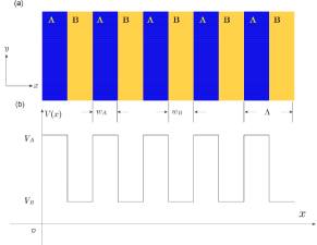
Let us consider a periodic sequence of MBLG SLs, which is perhaps the simplest sequence (see Fig. 1). Here, the width and the applied potential of the MLG on each unit are and , respectively, and the corresponding BLG parameters on each unit are and , respectively. According to Bloch’s theorem, for an infinite periodic structure , the electronic dispersion at any incident angle follows the relation
| (6) | |||||
where . Using , we can find the real solution of for passing bands. Otherwise, the non-existence of real indicates a band gap.
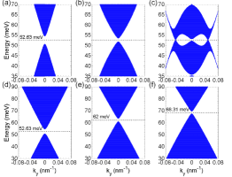
Figure 2 demonstrates the properties of electronic band gaps under different lattice parameters, indicating that there is a zero- gap in such periodic MBLG SLs. From Figs. 2(a)–2(c), it is apparent that the location of the zero- gap is independent of . In this case, it is positioned at approximately meV for a variety of . Under the same lattice parameters, the location of the zero- gap in periodic MBLG SLs is higher and lower than those of MLG TXMa2012 and BLG changan2013 SLs, respectively. Extra DPs may appear at for larger , as shown in Fig. 2(c); this will be discussed below. From Figs. 2(d)–2(f), the location of the zero- gap varies with changes in the ratio. For example, the zero- gaps are positioned at energy , , and meV for , , and , respectively.
The location of the zero- gap is determined by TXMa2012 . Note that should be replaced by for BLG. When the number of the MLG regions is equal to that of the BLG regions, the corresponding to can be easily found. Initially,
| (7) |
Then, for , Eq. (7) reduces to
| (8) |
The locations of the zero- gaps in Fig. 2 are in agreement with Eqs. (7) and (8).
We now consider a method to determine the locations of the extra DPs, which should obey the equation
| (9) |
Using Eq. (6), when ( is a positive integer), Eq. (9) above is satisfied. For , the zero- gap will close at the normal incident angle () with satisfying the condition
| (10) |
At oblique incidences () and when , the extra DPs appear. They are located at
| (11) |
The number of extra DPs can be obtained from Eq. (11) using the limiting condition: .
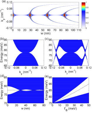
Extra DPs exist in the band structures of periodic MBLG SLs, which have already been shown in Fig. 2(c). In Fig. 3(a), the transmission probabilities of the centre of the zero- gap are plotted in order to find the extra DPs. In MLG SLs with periodic sequences, the charge carriers have perfect transmission at normal incidence and a DP is always positioned at the centre of the gap LGWang2010 . However, a different scenario occurs in the case of MBLG SLs with periodic sequences. As illustrated in Fig. 3(a), the zero- gap closes with a fixed period and extra paired DPs occur as increases; this is characterized by the large transmission probability in Fig. 3(a). In addition, it is important to notice that the DP does not exist at the normal incidence, and that it always has large reflection unless the gap is closed. From Eq. (10), the gap-closing period is nm for the parameters given in Fig. 3(a). Besides, extra DPs do not exist unless is larger than one period, as can be seen in Figs. 3(a)–3(c). Fig. 3(d) shows that the centre position of the zero- gap is independent of . The effect of the BLG’s on the band structure is shown in Fig. 3(e). It is apparent that the width of the zero- gap increases significantly as increases. The dotted dark line denotes the centre position of the zero- gap and satisfies a nonlinear relation [see Eq. (8)]. This differs from the linear relation obtained in the case of BLG SLs changan2013 .
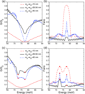
We next consider the total conductance and Fano factor (the ratio between the shot noise power and current) Datta1995 ; tworzydlo ; GF for different . In Fig. 4(a), the conductance of the zero- gap exhibits different values for different . For fixed , where nm, the conductance is approximately zero when the zero- gap opens. Specifically, a pair of extra DPs exist at the centre position of the zero- gap for nm [see Fig. 3(a)]. In this case, the conductance of this position is slightly higher than zero and the angular-average conductance curve forms a linear-like cone around the extra DPs. There is no unique DP at the zero- gap in MBLG SLs with periodic sequences, as is the case for MLG SL TXMa2012 ; PLzhao2011 ; XXGuo2011 . Therefore, the Fano factor at the centre position of the zero- gap can be removed from .
All the previous results were obtained by focusing on the one-mode wave function with longitudinal wave vector . Experimentally, this scenario can be realized using, for example, an adatom to create a wave function with a certain longitudinal wave vector. According to the result presented in Ref. duppen2013, , the two-mode wave function with no mixing can be considered as the primary contributor to the conductance or the Fano factor [in Ref. duppen2013, , see the values of and and compare them with and ]. Here, we ignore other complex transport processes that mix different wave function modes, and instead consider the contribution of the wave function with longitudinal wave vector sign() for , otherwise . The averaged conductance and Fano factor produced by both modes of the wave functions with and are plotted in Figs. 4(c) and 4(d), respectively. In these figures, the conductance curves exhibit several dips, whereas the Fano factor curves exhibit several small peaks, all of which are indicated by red dots. The groups of dips or peaks are located at and meV and are, therefore, separated; these separations are primarily caused by the zero- gaps of the wave functions with and . For the case of nm, the average of the conductance at approximately meV is increased compared with the zero conductance in Fig. 4(a), and the position of the conductance minimum is changed from to meV. Based on the above analysis, it may be concluded that the result obtained by focusing on the one-mode wave function is meaningful as a reflection of the transport properties of normal scenarios involving the two-mode wave function.
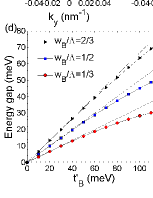
Finally, we consider another interesting effect. In the absence of an applied potential on the periodic MBLG SLs, the energy gap of the first two bands can be regularly tuned by controlling the ratio. The yellow regions in Figs. 5(a)–5(c) are occupied by electrons of the propagating mode, whereas the dark regions are occupied by electrons of both the propagating and evanescent modes. As illustrated in these figures, the gap width of the first two bands changes from , , to for , , and , respectively, under the given parameters. Further, the gap width is proportional to the ratio and roughly obeys
| (12) |
Figs. 5(d) and 5(e) show the correct range of Eq. (12). From Fig. 5(d), it is apparent that Eq. (12) accurately describes the regularity when is smaller than approximately meV in the case of nm, and the deviation is larger for larger . also affects the correctness of the above relation, as shown in Fig. 5(e). It is concluded that the actual gap width is smaller than the approximated result given by Eq. (12), which indicates that, as or increases, the effect of the MLG becomes stronger than that of the BLG. Based on the similarity between the band structures in Fig. 5 and those of the BLG, we may define as . As increases, the band structure becomes more similar to the parabolic band structure of BLG. For a periodic structure with alternating interlayer couplings in total two-layer graphene, Eq. (12) (which concerns the gap width) can be modified to
| (13) |
where is the interlayer coupling in the A regions, which are also BLG. The in MBLG SLs corresponds to the border between the propagating and evanescent wave modes, and this BLG border has been shown in Duppen and Peeters’ interesting work (see Ref. duppen2013, ). Furthermore, this border is tunable through adjustment of and and . Therefore, this may constitute a new method of controlling the electronic conductance.
In summary, we have studied the electronic band structures and transport properties of mono- and bi-layer graphene (MBLG) superlattices (SLs) with periodic sequences. The zero- gap is robust against the lattice constant , but sensitive to both the ratio of the potential widths and the interlayer coupling . The analytical condition determining the locations of extra Dirac points (DPs) () was presented and it was shown that the number of DPs increases as increases. Moreover, the conductance of the charge carriers in periodic MBLG SLs was investigated, and it was shown that the angular-average conductance curve forms a linear-like cone around the extra DPs, similar to that observed in the case of MLG SLs TXMa2012 . If no potential barriers are applied, the energy gap width of the first two bands or the average interlayer coupling is tunable through adjustment of and . This finding is important as regards research on interlayer coupling in two-layer graphene, and may constitute a new method of controlling the electronic conductance. Further related results will be reported in the near future. The findings of this and future studies will be useful for future research and applications concerning MBLG SLs.
T. Ma thanks CAEP for partial financial support. This work is supported by NSFCs (Grant. Nos. 11274275 and 11374034), and the National Basic Research Program of China (Grant Nos. 2011CBA00108 and 2012CB921602). We also acknowledge support from the Fundamental Research Funds for the Center Universities under Nos. 2015FZA3002 (L.-G. Wang) and 2014KJJCB26 (T. Ma).
References
- (1) Novoselov K. S., Geim A. K., Morozov S. V., Jiang D., Zhang Y., Dubonos S. V., Grigorieva I. V., and Firsov A. A., Science 306, 666 (2004).
- (2) Katsnelson M. I., Novoselov K. S., and Geim A. K., Nat. Phys. 2, 620 (2006).
- (3) Castro Neto A. H., Guinea F., Peres N. M. R., Novoselov K. S., and Geim A. K., Rev. Mod. Phys. 81, 109 (2009).
- (4) Ma T., Hu F. M., Huang Z. B., and Lin H.-Q., Appl. Phys. Lett. 97, 112504 (2010); Hu F. M., Ma T., Lin H.-Q., and Gubernatis J. E., Phys. Rev. B 84, 075414 (2011); Cheng S., Yu J., Ma T., and Peres N. M. R., Phys. Rev. B 91, 075410 (2015).
- (5) Peres N. M. R., Rev. Mod. Phys. 82, 2673 (2010).
- (6) Lee J. and Sachdev S., Phys. Rev. Lett.114, 226801 (2015).
- (7) Gregersen S. S., Pedersen J. G., Power S. R., and Jauho A.-P., Phys. Rev. B 91, 115424 (2015).
- (8) Bolotin K. I., Sikes K. J., Hone J., Stormer H. L., and Kim P., Phys. Rev. Lett.101, 096802 (2008).
- (9) Novoselov K. S., Geim A. K., Morozov S. V., Jiang D., Katsnelson M. I., Grigorieva I. V., Dubonos S. V., and Firsov A. A., Nature (London) 438, 197 (2005).
- (10) Purewal M. S., Zhang Y., and Kim P., Phys. Status Solidi B 243, 3418 (2006).
- (11) Brey L. and Fertig H. A., Phys. Rev. B 73, 195408 (2006); Brey L. and Fertig H. A., Phys. Rev. B 73, 235411 (2006).
- (12) Nakada K., Fujita M., Dresselhaus G., and Dresselhaus M. S., Phys. Rev. B 54, 17954 (1996).
- (13) Brey L. and Fertig H. A., Phys. Rev. Lett. 103, 046809 (2009).
- (14) Barbier M., Peeters F. M., and Vasilopoulos P., Phys. Rev. B 81, 075438 (2010).
- (15) Wang L.-G. and Zhu S.-Y., Phys. Rev. B 81, 205444 (2010); Wang L.-G. and Chen X., J. Appl. Phys. 109, 033710(2011).
- (16) Ma T., Liang C., Wang L.-G., and Lin H.-Q., Appl. Phys. Lett. 100, 252402 (2012).
- (17) Li C., Cheng H., Chen R., Ma T., Wang L.-G., Song Y., and Lin H.-Q., Appl. Phys. Lett. 103, 172106 (2013)
- (18) Bai C. and Zhang X., Phys. Rev. B 76, 075430 (2007).
- (19) Zhao P.-L. and Chen X., Appl. Phys. Lett. 99, 182108 (2011).
- (20) Guo X.-X., Liu D., and Li Y.-X., Appl. Phys. Lett. 98, 242101 (2011).
- (21) Zhao Q. F., Gong J. B., and Muller C. A., Phys. Rev. B 85, 104201 (2012).
- (22) Zhang Z.-R, Li H.-Q, Gong Z.-J, Fan Y.-C, Zhang T.-Q, Appl. Phys. Lett. 101, 252104 (2012).
- (23) Barbier M., Vasilopoulos P., Peeters F. M. and Pereira J. M., Phys. Rev. B 79, 155402 (2009).
- (24) Nilsson J., Castro Neto A. H., Guinea F., and Peres N. M. R., Phys. Rev. B 76, 165416 (2007).
- (25) Nakanishi T., Koshino M., and Ando T., Phys. Rev. B 82, 125428 (2010); Koshino M., Nakanishi T., and Ando T., Phys. Rev. B 82, 205436 (2010).
- (26) Wang Y., J. Appl. Phys. 116, 164317(2014).
- (27) Giannazzo F., Deretzis I., Magna A. L., Roccaforte F., and Yakimova R., Phys. Rev. B 86, 235422 (2012).
- (28) Nilsson J., Castro Neto A. H., Peres N. M. R., and Guinea F., Phys. Rev. B 73, 214418 (2006).
- (29) McCann E., Phys. Rev. B 74, 161403(R) (2006).
- (30) Snyman I. and Beenakker C. W. J., Phys. Rev. B 75, 045322 (2007).
- (31) Zarenia M., Vasilopoulos P., and Peeters F. M., Phys. Rev. B 85, 245426 (2012)
- (32) Yin L.-J, Li S.-Y, Qiao J.-B, Zuo W.-J and He L., arXiv:1509.04405 (unpublished).
- (33) Datta S., Electronic Transport in Mesoscopic Systems (Cambridge University Press, Cambridge, England, 1995).
- (34) Tworzydlo J., Trauzettel B., Titov M., Rycerz A., and Beenakker C. W. J., Phys. Rev, Lett. 96, 246802 (2006).
- (35) G and F are calculated by and , where ( denotes the length of graphene stripe in the y direction).
- (36) Duppen B. V., and Peeters F. M., Phys. Rev. B 87, 205427 (2013).