Multi-beam 4 GHz Microwave Apertures Using Current-Mode DFT Approximation on 65 nm CMOS

Viduneth Ariyarathna    Sunera Kulasekera    Arjuna Madanayake    Kye-Shin Lee V. Ariyarathna, S. Kulasekera, A. Madanayake, and K.-S. Lee are with the Department of Electrical and Computer Engineering, University of Akron, Akron, OH, USA 44325-3904. E-mail: arjuna@uakron.edu    Dora Suarez D. Suarez is with the Signal Processing Group, Departamento de Estatística, UFPE, Brazil.    R. J. Cintra R. J. Cintra is with the Signal Processing Group, Departamento de Estatística, Universidade Federal de Pernambuco; Equipe Cairn, IRISA/INRIA, Université de Rennes 1, Rennes, France; LIRIS, and Institut National des Sciences Appliquées, Lyon, France. E-mail: rjdsc@stat.ufpe.org    Fábio M. Bayer F. M. Bayer is with the Departamento de Estatística, Universidade Federal de Santa Maria, Brazil.    Leonid Belostotski L. Belostotski is with the Department of Electrical and Computer Engineering, University of Calgary, Calgary, AB T2N 1N4, Canada.
Abstract

A current-mode CMOS design is proposed for realizing receive mode multi-beams in the analog domain using a novel DFT approximation. High-bandwidth CMOS RF transistors are employed in low-voltage current mirrors to achieve bandwidths exceeding 4 GHz with good beam fidelity. Current mirrors realize the coefficients of the considered DFT approximation, which take simple values in $\{0,\pm 1,\pm 2\}$ only. This allows high bandwidths realizations using simple circuitry without needing phase-shifters or delays. The proposed design is used as a method to efficiently achieve spatial discrete Fourier transform operation across a ULA to obtain multiple simultaneous RF beams. An example using 1.2 V current-mode approximate DFT on 65 nm CMOS, with BSIM4 models from the RF kit, show potential operation up to 4 GHz with eight independent aperture beams.

Keywords
Analog, arrays, beamforming, aperture, multibeam.


1 Introduction

The formation of multiple orthogonal radio-frequency (RF) beams are a quintessential example of antenna arrays [1, 2]. There are applications for multi-beam arrays, such as wireless communications, radar, radio astronomy, and space imaging. Alternative to phased-arrays [3] that achieve a single steerable beam, multiple simultaneous RF beams—directed at fixed directions—are achieved using a spatial discrete Fourier transform (DFT) operation across a uniformly-spaced array [4, 5]. In digital radar, multi-beams are achieved by digitizing the intermediate frequency (IF) signals from each element receiver, which are connected to the array. Sampling is followed by an application of the $N$-point spatial DFT computed via a fast Fourier transform (FFT) on a per-frame basis [4, 5].

The use of an 8-point approximate DFT, implemented by means of a fast algorithm [6], where DFT-beams have been closely emulated using a matrix of Gaussian integer weights, allows multi-beams using relatively simple active RF circuits. Approximate transformations are linear transformations of low computational cost offering close results to that from the exact transformation. The realization of multi-beams in analog by mean of a DFT approximation using microwave circuits exploits the high-bandwidth of current-mode CMOS integrated circuits. The approximate DFT achieves RF beams that are nearly identical to DFT-beams albeit without a Butler Matrix. That is, the analog circuit becomes quite simple to design owing to the use of current mirrors having weights over the set $\mathcal{P}=\{0,\pm 1,\pm 2\}$ only. We show that such an approximation can be efficiently realized at 4 GHz or more of bandwidth using analog IC designs. Fig. 1 shows the overview of the aperture array, where $N$ elements makeup a uniformly-spaced linear array (ULA) with spacing $\Delta x$. The elements (e.g., Vivaldi or spiral antennas) are amplified and quadrature down-converted or fed through a quadrature hybrid (QH) to achieve complex inputs for the 8-point DFT approximation.

Refer to captionV/I$v_{in}$V/I$I_{k,Q}$ $\psi_{d}$Analog ADFT$v_{in}$Antenna array00$v_{n}\in\mathbb{C}$ $A_{0}$ $A_{N-1}$ $v_{n}\in\mathbb{C}$ $N-1$ $V_{0}$ $V_{N-1}$ $w_{k}$ $I_{k,I}$
Figure 1: Analog RF 8-beam aperture using a spatial 8-point DFT approximation.

2 8-point Approximate DFT Multi-Beam Matrix

Recall that a DFT is a discrete orthogonal transformation that transforms an input vector $\mathbf{v}=\begin{bmatrix}v_{0}(t)&v_{1}(t)&\cdots&v_{N}(t)\end{bmatrix}^{\top}$ to an output vector with $N$ spectral coefficients, denoted by $\mathbf{V}=\begin{bmatrix}V_{0}(t)&V_{1}(t)&\cdots&V_{N}(t)\end{bmatrix}^{\top}$ [7], each corresponding to a far-field RF beam for $N$ element arrays when $v_{k}(t)=x_{I}(t)+jx_{Q}(t)\in\mathbb{C}$ consist of in-phase $(x_{I}(t))$ and quadrature $(x_{Q}(t))$ antenna feeds from a QH component per array element, and where $V_{k}(t)=\sum_{n=0}^{N-1}v_{n}(t)\cdot\omega_{N}^{kn},\quad k=0,1,\ldots,N-1,$ where $j=\sqrt{-1}$ and $\omega_{N}=\exp\left\{-\frac{2\pi j}{N}\right\}$ is the $N$th root of unity. In matrix form, $\mathbf{V}=\mathbf{F}_{N}\cdot\mathbf{v}$ and $\mathbf{v}=\mathbf{F}_{N}^{-1}\cdot\mathbf{V}=\frac{1}{N}\cdot\mathbf{F}_{N}^{*}\cdot\mathbf{V}$, where $\mathbf{F}_{N}$ is the DFT transformation matrix whose $(i,k)$th element is $f_{i,k}=\omega_{N}^{(i-1)(k-1)}$, for $i,k=1,2,\ldots,N$ and the superscript  denotes the transposed conjugation (Hermitian). Classical radar apertures obtain multi-beams using a Butler Matrix realization of the DFT. For the derivation of DFT approximations, we consider the set $\mathcal{Q}=\Big{\{}z\in\mathbb{C}\,:\,\Re\{z\}\in\mathcal{P}\land\Im\{z\}\in\mathcal{P}\Big{\}}$ for the matrix entries of the DFT approximation matrices. Parametric optimization, which minimizes the Frobenius norm, over the set $\mathcal{Q}$ leads to an 8-point DFT approximation having near-orthogonality and low circuit complexity. The optimal elements for the parametric approximation of $\mathbf{F}_{8}$ are $1$, $(1-j)/2$, and $-j$. Thus, the resulting approximate DFT matrix contains only Gaussian integer entries:

𝐅^8=12[ \Let@\restore@math@cr\default@tag 2 2 2 2 2 2 2 2 2 -1j -2j --1j −2 +-1j 2j +1j 2 -2j −2 2j 2 -2j −2 2j 2 --1j 2j -1j −2 +1j -2j +-1j 2 −2 2 −2 2 −2 2 −2 2 +-1j -2j +1j −2 -1j 2j --1j 2 2j −2 -2j 2 2j −2 -2j 2 +1j 2j +-1j −2 --1j -2j -1j ]subscript^𝐅812delimited-[] \Let@\restore@math@cr\default@tag 2 2 2 2 2 2 2 2 2 -1j -2j --1j −2 +-1j 2j +1j 2 -2j −2 2j 2 -2j −2 2j 2 --1j 2j -1j −2 +1j -2j +-1j 2 −2 2 −2 2 −2 2 −2 2 +-1j -2j +1j −2 -1j 2j --1j 2 2j −2 -2j 2 2j −2 -2j 2 +1j 2j +-1j −2 --1j -2j -1j \displaystyle\hat{\mathbf{F}}_{8}=\frac{1}{2}\cdot\left[\hbox{}\,\vbox{\Let@\restore@math@cr\default@tag\halign{\hfil$\m@th\scriptstyle#$&&\thickspace\hfil$\m@th\scriptstyle#$\cr 2&2&2&2&2&2&2&2\\ 2&1-j&-2j&-1-j&-2&-1+j&2j&1+j\\ 2&-2j&-2&2j&2&-2j&-2&2j\\ 2&-1-j&2j&1-j&-2&1+j&-2j&-1+j\\ 2&-2&2&-2&2&-2&2&-2\\ 2&-1+j&-2j&1+j&-2&1-j&2j&-1-j\\ 2&2j&-2&-2j&2&2j&-2&-2j\\ 2&1+j&2j&-1+j&-2&-1-j&-2j&1-j\\ }}\,\right]

The above 8-point approximate DFT matrix 𝐅^8subscript^𝐅8\hat{\mathbf{F}}_{8} preserves the symmetry of the DFT and has null multiplicative complexity—a salient property that allows realization using current-mode circuits having integer multiplications of current values that map neatly into multiples of identical 1:1 mirrors on an analog IC. Let 𝐈nsubscript𝐈𝑛\mathbf{I}_{n} be the identity matrix of order n𝑛n and 𝐁n=[ \Let@\restore@math@cr\default@tag 1 1 1 −1 ]𝐈n/2subscript𝐁𝑛tensor-productdelimited-[] \Let@\restore@math@cr\default@tag 1 1 1 −1 subscript𝐈𝑛2\mathbf{B}_{n}=\left[\hbox{}\,\vbox{\Let@\restore@math@cr\default@tag\halign{\hfil$\m@th\scriptstyle#$&&\thickspace\hfil$\m@th\scriptstyle#$\cr 1&1\\ 1&-1\crcr}}\,\right]\otimes\mathbf{I}_{n/2}, where tensor-product\otimes denotes the Kronecker product. Matrix factorization techniques leads to an algorithm for mapping to analog circuits [7]. In particular, 𝐅^8subscript^𝐅8\mathbf{\hat{F}}_{8} admits the following factorization:

$\displaystyle\mathbf{\hat{F}}_{8}=$ $\displaystyle\mathbf{P}\times\operatorname{diag}\big{(}\mathbf{I}_{2},\mathbf{A}_{1},\mathbf{A}_{3}\big{)}\times\mathbf{D}_{2}\times\operatorname{diag}\big{(}\mathbf{B}_{2},\mathbf{I}_{2},\mathbf{A}_{4}\big{)}$
$\displaystyle\times\mathbf{D}_{1}\times\operatorname{diag}\big{(}\mathbf{B}_{4},\mathbf{A}_{2}\big{)}\times\mathbf{B}_{8},$

where 𝐀1=[ \Let@\restore@math@cr\default@tag 1 −1 1 1 ]subscript𝐀1delimited-[] \Let@\restore@math@cr\default@tag 1 −1 1 1 \mathbf{A}_{1}=\left[\hbox{}\,\vbox{\Let@\restore@math@cr\default@tag\halign{\hfil$\m@th\scriptstyle#$&&\thickspace\hfil$\m@th\scriptstyle#$\cr 1&-1\\ 1&1\crcr}}\,\right], 𝐀2=[ \Let@\restore@math@cr\default@tag 1 1 1 1 1 −1 ]subscript𝐀2delimited-[] \Let@\restore@math@cr\default@tag 1 1 1 1 1 −1 \mathbf{A}_{2}=\left[\hbox{}\,\vbox{\Let@\restore@math@cr\default@tag\halign{\hfil$\m@th\scriptstyle#$&&\thickspace\hfil$\m@th\scriptstyle#$\cr 1&&&\\ &1&&1\\ &&1&\\ &1&&-1\crcr}}\,\right], 𝐀3=[ \Let@\restore@math@cr\default@tag 1 −1 −1 1 1 1 1 1 ]subscript𝐀3delimited-[] \Let@\restore@math@cr\default@tag 1 −1 −1 1 1 1 1 1 \mathbf{A}_{3}=\left[\hbox{}\,\vbox{\Let@\restore@math@cr\default@tag\halign{\hfil$\m@th\scriptstyle#$&&\thickspace\hfil$\m@th\scriptstyle#$\cr 1&-1&&\\ &&-1&1\\ 1&1&&\\ &&1&1\crcr}}\,\right], 𝐀4=[ \Let@\restore@math@cr\default@tag 1 1 1 1 1 −1 1 −1 ]subscript𝐀4delimited-[] \Let@\restore@math@cr\default@tag 1 1 1 1 1 −1 1 −1 \mathbf{A}_{4}=\left[\hbox{}\,\vbox{\Let@\restore@math@cr\default@tag\halign{\hfil$\m@th\scriptstyle#$&&\thickspace\hfil$\m@th\scriptstyle#$\cr 1&&&1\\ &1&1&\\ &1&-1&\\ 1&&&-1\crcr}}\,\right], 𝐃1=diag( \Let@\restore@math@cr\default@tag 1, 1, 1, 1, 1, /12, 1, /12 )subscript𝐃1diag \Let@\restore@math@cr\default@tag 1, 1, 1, 1, 1, /12, 1, /12 \mathbf{D}_{1}=\operatorname{diag}(\hbox{}\,\vbox{\Let@\restore@math@cr\default@tag\halign{\hfil$\m@th\scriptstyle#$&&\thickspace\hfil$\m@th\scriptstyle#$\cr 1,&1,&1,&1,&1,&1/2,&1,&1/2\crcr}}\,), 𝐃2=diag( \Let@\restore@math@cr\default@tag 1, 1, 1, j, 1, j, j, 1 )subscript𝐃2diag \Let@\restore@math@cr\default@tag 1, 1, 1, j, 1, j, j, 1 \mathbf{D}_{2}=\operatorname{diag}(\hbox{}\,\vbox{\Let@\restore@math@cr\default@tag\halign{\hfil$\m@th\scriptstyle#$&&\thickspace\hfil$\m@th\scriptstyle#$\cr 1,&1,&1,&j,&1,&j,&j,&1\crcr}}\,), 𝐏=[ \Let@\restore@math@cr\default@tag e1 |e5 |e3 |e6 |e2 |e8 |e4 |e7 ]𝐏superscriptdelimited-[] \Let@\restore@math@cr\default@tag e1 |e5 |e3 |e6 |e2 |e8 |e4 |e7 top\mathbf{P}=\left[\hbox{}\,\vbox{\Let@\restore@math@cr\default@tag\halign{\hfil$\m@th\scriptstyle#$&&\thickspace\hfil$\m@th\scriptstyle#$\cr\mathbf{e}_{1}&\big{|}\,\mathbf{e}_{5}&\big{|}\,\mathbf{e}_{3}&\big{|}\,\mathbf{e}_{6}&\big{|}\,\mathbf{e}_{2}&\big{|}\,\mathbf{e}_{8}&\big{|}\,\mathbf{e}_{4}&\big{|}\,\mathbf{e}_{7}\crcr}}\,\right]^{\top} is a permutation matrix, and 𝐞isubscript𝐞𝑖\mathbf{e}_{i} is the 8-point column vector with element 1 at the i𝑖ith position and 0 elsewhere.

3 8-beam 4 GHz DFT Approximation in 65 nm CMOS

3.1 Antenna Front-End

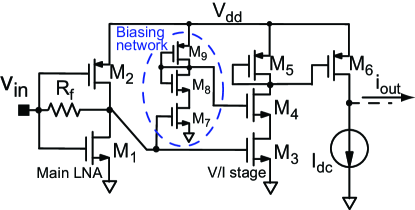
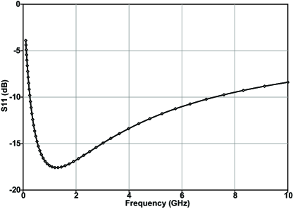
A conventional inverter-based shunt feedback LNA, shown in Fig. 2(a), is employed. The input signal, $v_{\text{in}}$, from each antenna is applied to the gates of $M_{1}$ and $M_{2}$, forming the main LNA, whose $S_{11}$, displayed in Fig. 2(b), is set with $R_{f}$ and the transconductances of $M_{1,2}$. The cascoded transistors $M_{3,4}$ are used to increase the impedance at the drain of $M_{5}$ so that most of the small-signal current flows into the $M_{5,6}$ current mirror. The circuit consisting of $M_{\text{3-6}}$ forms a voltage-to-current (V/I) conversion stage. A DC current source $I_{\text{dc}}$ reduces the DC component of the $i_{\text{out}}$ current. The gate bias for $M_{4}$ is provided by a biasing network consisting of $M_{\text{7-9}}$, which are scaled versions of $M_{\text{3-5}}$. The LNA draws $26.25\,\mbox{mA}$ from a 1.2 V DC supply.

Refer to caption
Refer to caption
Figure 2: 65 nm 1.2 V CMOS LNA with current output $i_{out}$ (top); amplifier $|S_{11}|$[dB] better than $-10$ dB up to 7 GHz (bottom).
Refer to captionPMOSNMOS$Re\{\hat{F}_{8(8,i)}\}(I_{bias}+i_{i}(t))$ $i_{1}(t)$ $i_{5}(t)$ $i_{6}(t)$ $i_{8}(t)$NMOSNMOSNMOSNMOSNMOSNMOS$\alpha$ $\beta$ $\alpha-\beta$ $I_{out}$ $\beta=i_{2}(t)+2i_{5}(t)+i_{8}(t)$ $(a)$ $(b)$ $I_{out}$ $L_{2}=60nm$ $W_{2}=.7um$ $I_{bias}+i_{i}(t)$ $V_{DD}$ $\frac{W_{3}}{L_{3}}$ $\frac{W_{4}}{L_{4}}$ $\frac{W_{4}}{L_{4}}$PMOS1:1$I_{bias}+i_{i}(t)$ $Re\{\hat{F}_{8(1,i)}\}(I_{bias}+i_{i}(t))$ $Re\{\hat{F}_{8(2,i)}\}(I_{bias}+i_{i}(t))$ $\alpha=2i_{1}(t)+i_{4}(t)+i_{6}(t)$ $\frac{W_{3}}{L_{3}}$ $i_{2}(t)$ $i_{4}(t)$ $I_{bias}+i_{i}(t)$ $I_{bias}+i_{i}(t)$ $V_{DD}$ $\frac{W_{1}}{L_{1}}$ $\frac{W_{2}}{L_{2}}$ $W_{1}=.9um$ $L_{1}=150nm$ $I_{bias}+i_{i}(t)$ $\frac{W_{1}}{L_{1}}$ $\frac{W_{2}}{L_{2}}$ $(c)$ $(d)$ $(e)$ $L_{3}=60nm$ $L_{4}=60nm$ $W_{3}=3.7um$ $W_{4}=4um$
Figure 3: Current mode implementation of the 8-point DFT approximation using 65 nm CMOS RF NMOS/PMOS mirrors.
Refer to caption$2~{}GHz$ $1~{}GHz$ $4~{}GHz$
Figure 4: Polar response patterns for current outputs at $1$, $2$, and $4$ GHz.

3.2 Current Mode Analog 8-point Approximate DFT

The matrix $\hat{\mathbf{F}}_{8}$ is realized in current mode to increase operational bandwidth. The signals from each LNA+secondary amplifier at the antennas (Fig. 1) are converted to output currents $i_{\text{out}}$. Eight such small-signal current outputs form the input signals for the current-mode realization of the discussed 8-point approximate DFT. The real and imaginary components of the considered approximate DFT matrix are realized separately. Fig. 3(a) shows a NMOS current copier used to realize one column of the DFT approximation matrix (real part). Fig. 3(b) shows the PMOS based current subtractor needed for negative valued entries of the DFT approximation matrix. Example building blocks for the NMOS and PMOS current combiners in Fig. 3(a-b) are provided in Fig. 3(c-d), respectively. The DC bias current for the NMOS mirror in Fig. 3(c) is $I_{\text{bias}}=100~{}\mu A$. An example of one row of the 8-point approximate DFT (row 4) is shown in Fig. 3(e). All signal currents are assumed to be small (1–10%) compared to DC bias currents. Each current mirror is designed using the low-voltage cascode topology [8]. The technology used is 65 nm GP CMOS, and all transistors are from the RF kit, with supply voltage 1.2 V. Simulations are in Cadence Spectre and employ BSIM4 RF transistor models.

3.3 BSIM4 Array Patterns

The Cadence designs were simulated at frequencies $f\in\{1,2,4\}$ GHz. The input currents were maintained at $2\mu A$ peak-to-peak. The time-domain response was simulated, in steady state, and the peak-to-peak values were noted. The simulated small-signal output currents from the 8-point DFT approximation outputs were used to compute the polar response patterns for each current mode circuit for three frequencies in Fig. 4. The polar patterns obtained from the BSIM4 models of the discussed DFT approximation is very close to the expected ideal polar patterns linked to the theoretical 8-point DFT approximation. At higher frequencies, from the low-pass effects of the current mirrors due to dominant parasitic poles of the CMOS circuit, the pattern deviates noticeably (not shown here). The 8-point approximate DFT provides far-field receive beams at directions $90.0^{\circ}$, $48.5^{\circ}$, $30.0^{\circ}$, $14.5^{\circ}$, $0.0^{\circ}$, $-14.5^{\circ}$, $-30.0^{\circ}$, and $-48.5^{\circ}$ measured from the array.

4 Conclusion

The discussed DFT approximation is a numerical efficient method for the approximate DFT evaluation, and requires only small Gaussian integer valued weights. A multi-beam aperture algorithm and analog RF CMOS implementation for the 8-point approximate DFT was proposed, designed, simulated and evaluated, for beamforming at bandwidths up to 4 GHz using ULAs of wideband elements. The analog approximate DFT circuit was designed using 65 nm GP CMOS employing RF transistors, with low-voltage current mirrors for maximum peak-peak swings and bandwidth. Cadence BSIM4 models verify the aperture provides eight RF beams up to 4 GHz when supplied with 1.2 V DC.

References

  • [1] S. Patnaik, S. Kalia, B. Sadhu, M. Sturm, M. Elbadry, and R. Harjani, “An 8 GHz multi-beam spatio-spectral beamforming receiver using an all-passive discrete time analog baseband in 65 nm CMOS,” in Custom Integrated Circuits Conference (CICC), 2012 IEEE, Sept 2012, pp. 1–4.
  • [2] S. Kalia, S. A. Patnaik, B. Sadhu, M. Sturm, M. Elbadry, and R. Harjani, “Multi-beam spatio-spectral beamforming receiver for wideband phased arrays,” Circuits and Systems I: Regular Papers, IEEE Transactions on, vol. 60, no. 8, pp. 2018–2029, Aug 2013.
  • [3] E. Klumperink, D. Leenaerts, and G. Rebeiz, “Beamforming techniques and RF transceiver design,” in Solid-State Circuits Conference Digest of Technical Papers (ISSCC), 2012 IEEE International, Feb 2012, pp. 498–499.
  • [4] S. Ellingson and W. Cazemier, “Efficient multibeam synthesis with interference nulling for large arrays,” Antennas and Propagation, IEEE Transactions on, vol. 51, no. 3, pp. 503–511, March 2003.
  • [5] J. Coleman, “A generalized FFT for many simultaneous receive beams,” Naval Research Lab, Tech. Rep., 2007, NRL/MR/5320–07-9029.
  • [6] D. Suarez, R. J. Cintra, F. M. Bayer, A. Sengupta, S. Kulasekera, and A. Madanayake, “Multi-beam RF aperture using multiplierless FFT approximation,” Electronics Letters, vol. 50, no. 24, pp. 1788–1790, 2014.
  • [7] R. E. Blahut, Fast Algorithms for Signal Processing.   Cambridge University Press, 2010.
  • [8] B. Razavi, Design of Analog CMOS Integrated Circuits, ser. McGraw-Hill Higher Education.   Tata McGraw-Hill, 2002.