Giant magneto-photoelectric effect in suspended graphene
Abstract
We study the optical response of a suspended graphene field-effect transistor in magnetic fields of up to 9 T (quantum Hall regime). With an illumination power of only 3 W, we measure a photocurrent of up to 400 nA, corresponding to a photo-responsivity of 0.14 A/W, which we believe to be the highest value ever measured in single-layer graphene. We estimate that every absorbed photon creates more than 8 electron-hole pairs, which demonstrates highly effective carrier multiplication. As suggested by the dependence of the photocurrent on gate voltage and magnetic field, we propose a ballistic two-stage mechanism where the incident photons create primary charge carriers which then excite secondary charge carriers in the chiral edge states via Auger-type inelastic Coulomb scattering processes at the graphene edge.
pacs:
72.80.Vp, 78.67.Wj, 65.80.Ck.For many years, the famous paper by W.B. Shockley and H.-J. Queisser from 1961 has been the standard for assessing the maximum efficiency of semiconductor solar cells Shockley61 . In brief, the main argument is based on the assumption that photons with energies below the band-gap of the semiconductor are not absorbed while the excess energy of photons above the band-gap is dissipated as heat and not converted into electric energy. Recently, however, the Shockley-Queisser limit has been under close scrutiny, as some of the limiting factors may be overcome using novel, tailored materials and mechanisms, which were not envisioned 50 years ago. One such mechanism, which recently received great attention, is carrier multiplication Schaller04 ; Chan12 ; Beard07 ; Wang10 ; Congreve13 ; Tielrooij13 ; Ploetzing14 ; Mittendorff15 : Charge carriers, which are optically excited with a surplus energy, can relax by exciting electron-hole pairs, effectively turning a single photon into two or more electron-hole pairs that can drive an external circuit.
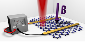
For optical or infrared absorption, the two-dimensional crystal graphene is a promising material, as its pseudo-relativistic energy-momentum relation at low energies (where is the Fermi velocity) gives rise to a broad absorption bandwidth. On the other hand, the absence of an energy gap seems to rule out the usual mechanism for charge separation in semiconductor solar cells via a built-in electrical potential gradient, and graphene -junctions are challenging to fabricate Gabor11 ; Williams07 . Recently, some of us proposed to employ the magneto-photoelectric effect along a graphene fold or edge to achieve charge separation Queisser13 using an applied magnetic field instead of an electrical potential gradient, see Figure 1.
Apart from the high charge carrier mobility and the broad absorption bandwidth, which remains true for the edge states in a magnetic field, graphene has a number of further interesting properties for magneto-photocurrent generation. For example, the cyclotron radius of a pseudo-relativistic electronic excitation in graphene
| (1) |
with the elementary charge and an energy corresponding to, say, room temperature within a magnetic field of 4 Tesla (see below) is 6 nm and thus well below the mean free path. Furthermore, in addition to this classical length scale, the magnetic (Landau) length is of the same order – which shows that quantum effects have to be taken into account. The third advantage of graphene lies in the relatively strong Coulomb interaction: In analogy to quantum electrodynamics (QED), we can construct an effective fine-structure constant in graphene
| (2) |
and find that this coupling strength is much larger than due to . Intuitively speaking, the charge carriers are much slower than the speed of light and thus have more time to interact. These comparably strong interactions will be important for charge carrier multiplication discussed below foot-absorption .
Motivated by the predictions in Queisser13 , here we experimentally investigate the photocurrent generation in suspended graphene in a quantizing magnetic field. We start from commercially available CVD graphene, transferred to a 285 nm SiO2-on-Si substrate. The silicon substrate is highly doped and is used as a back gate electrode. Using photolithography and an oxygen plasma, the graphene is patterned into bars of m width. Afterwards, Ti/Au (5/100 nm) electrodes are defined by electron beam lithography. The contacts cover the whole width of the graphene bars and are separated by 660 nm. In a subsequent etching step using hydrofluoric acid, nm of SiO2 are removed below the graphene, which creates a suspended field-effect transistor structure Bolotin08 ; Sommer15 . A scanning electron micrograph of the suspended graphene (taken after the photocurrent measurements) is shown in Fig. 2 (a).
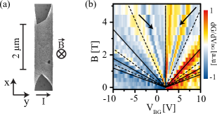
Our measurement setup consists of a confocal microscope inside a liquid helium cryostat, which allows us to measure at a temperature of 4.2 K and in magnetic fields of up to 9 T. After cooling down, the graphene is cleaned in-situ by a current annealing step Moser07 ; Bolotin08 . To check the quality of the graphene, we perform transconductance measurements d/d in different magnetic fields. Here is the conductance of the graphene channel and is the bias applied to the back gate to control the charge carrier density in the graphene. The resulting Shubnikov-de Haas oscillations are shown in Fig. 2 (b). The Dirac point lies at , so that the Landau levels fan out from this point. The expected fan diagram [dotted and solid lines in Fig. 2 (b)] is calculated from the geometric capacitance and the theoretical energy spectrum of single layer graphene , where is the Landau level index. The good agreement with the experimental data confirms the geometric capacitance and shows that the graphene is suspended in a single layer. The Shubnikov-de Haas oscillations can be observed at magnetic fields as low as 0.5 T, indicating a mobility of Bolotin08 . At magnetic fields above 1 T, additional plateaus appear, showing at least partial splitting of the zeroth Landau level. This effect is often observed in high-quality samples and is frequently attributed to electron-electron interactions Du09 ; Bolotin09 ; Young12 .
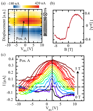
Next we investigate the photocurrent generation in suspended graphene. For this purpose, we use the confocal microscope and a near-infrared laser with a wavelength of 972 nm and a spot diameter of roughly 1.5 m. The illumination power is 3 W and we use a low-impedance () current amplifier to directly measure the photocurrent. The laser spot is positioned in between the two gold contacts. Since the distance between the contacts is less than the spot diameter, only the spatial dependence perpendicular to the current flow can be resolved. Figure 3 (a) shows the generated photocurrent at T, well within the quantum Hall regime. The photocurrent is found to be symmetric around the Dirac point, but there is a clear change in polarity, depending on which edge of the graphene is illuminated. This is in agreement with the magnetic-field induced chirality of the charge-carrier motion (see below).
As Fig. 3 (a) shows, the measured photocurrent reaches surprisingly high values of over 400 nA at the Dirac point when illuminating the upper edge [position A in Fig. 3 (a)]. Considering the illumination power of 3 W, this corresponds to a photo-responsivity of 0.14 A/W, a value more than an order of magnitude higher than reported previously for single layer graphene devices Nazin10 ; Freitag13 and comparable to the responsivity of commercially available photodiodes. Assuming that the entire laser spot illuminates graphene and taking into account the absorption of graphene of Nair08 , this high current of 400 nA implies that for every absorbed photon 8 electron-hole pairs are created. We believe that this is the highest value of charge carrier multiplication observed in graphene as well as in any optically excited semiconductor system so far Schaller04 ; Chan12 ; Beard07 ; Wang10 ; Congreve13 ; Tielrooij13 ; Ploetzing14 ; Mittendorff15 .
The gate-voltage dependence of the magneto-photocurrent at different magnetic fields is shown in Fig. 3 (c). The photocurrent at zero magnetic field (black line) features a step at the Dirac point, often observed at or graphene-metal junctions, and commonly attributed to thermoelectric effects Gabor11 . For an applied magnetic field, the step at the Dirac point turns into a peak, whose height and width first increases with increasing magnetic fields but later (for T) decreases again, see Fig. 3 (b) foot1 . This is in strong contrast to the expected oscillatory behavior of usual (diffusive) thermoelectric effects in the quantum Hall regime Zuev09 ; Checkelsky09 ; Jonson84 ; Girvin82 , see also foot-nazin . Furthermore, we find a distinct polarization dependence (not shown here Sonntag14 ), which is also not expected for a thermoelectric response foot2 .
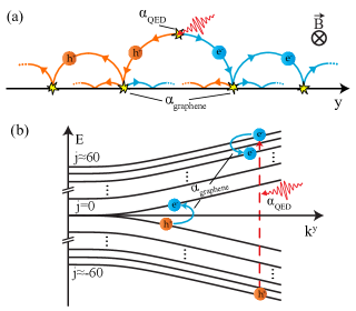
Based on these observations and our previous work Queisser13 , we propose the following two-stage ballistic mechanism (sketched in Fig. 4) based on the creation of primary and secondary charge carriers and their transport far from equilibrium: With the universal absorption probability , the incident photon of energy eV creates a pair of an electron and a hole with equal energies of and opposite momenta due to energy-momentum conservation. However, the momentum of the electron (or hole) can point in both directions with equal probability and thus no net current is generated at this stage. Since the wavelength of the electron or hole excitations is much smaller than the classical cyclotron radius (1) of approximately 150 nm at 4 T, we can treat the propagation semi-classically. Thus, the electron and hole excitations describe circular trajectories with the cyclotron radius (1) until they reach the metallic contacts or they are scattered by defects or the graphene edge.
A net current is induced when at least one of the carriers is reflected at the graphene edge, where the originally random direction of charge separation is transformed into a determined directionality/chirality as in Figure 4, where holes move to the left and electrons to the right. The current runs into opposite directions at the upper and lower edge, which explains the position dependence in Fig. 3 (a). This simple picture also accounts for the observed dependence on the magnetic field: If the magnetic field is too small, the radius (1) is much larger than the distance between the metallic contacts and thus the trajectories are not bent enough to control (rectify) the direction of charge separation efficiently. For intermediate field strengths of around 4 T, the circular diameter of 300 nm fits well into the graphene sample and thus (directed) charge separation is most efficient. If the magnetic field becomes too large, however, this diameter shrinks and thus the incident photon must be absorbed very near the edge when the circle is supposed to intercept the edge – i.e., the effective absorption area shrinks. However, as explained above, these primary electron-hole pairs (directly created by the incident laser photons) cannot account for the observed current. The observed carrier multiplication can be explained by inelastic scattering at the graphene edge. Neglecting dielectric and screening effects in our order-of-magnitude estimate, we consider the Coulomb interaction Hamiltonian
| (3) |
with the charge density operator , where is the two-component (spinor) field operator. In principle, this non-linear interaction Hamiltonian could also induce carrier multiplication in translationally invariant (bulk) graphene, but this process is strongly suppressed due to energy-momentum conservation foot-phase-space . This supression can be diminished by the coupling to phonons, defects, or a magnetic field, etc., and carrier multiplication has been observed in such scenarios Tielrooij13 ; Ploetzing14 ; Mittendorff15 ; Wendler14 .
Here, we consider the inelastic reflection at the graphene edge (see Fig. 4) where the perpendicular momentum is not conserved and thus we expect strong carrier multiplication effects. Since the primary electron or hole excitation has a comparably large , we approximate it by a plane wave and similarly for the outgoing excitation after inelastic scattering at the edge. In order to deal with well-defined modes for the secondary excitations, we consider the fold modes discussed in Queisser13 , but other models yield very similar results. Furthermore, a closer inspection of Fig. 2 (a) suggests that the graphene edge is indeed folded (at least over a wide range) such that the fold modes should be a good description. Assuming that the edge runs along the -axis, in the lowest band, these modes behave as for large , where denotes the electron and the hole excitation. These modes are localized (in -direction) at the fold and propagate along it (in -direction) with nearly . Their transverse extent is determined by where is the curvature radius of the graphene fold (roughly between 10 and 20 nm).
Via standard perturbation theory with respect to the interaction Hamiltonian (3), we calculate the amplitude (matrix element) for Auger-type inelastic scattering of a primary excitation from to while creating a secondary electron-hole pair with . The conservation of energy and momentum in -direction determines the wave-numbers uniquely and the remaining matrix element reads (for large )
| (4) | |||||
where is the momentum transfer and quantifies the particle-hole asymmetry. In the perpendicular case , we get and thus such that this asymmetry disappears and the above formula simplifies strongly. The total probability for this Auger-type carrier multiplication process can then be estimated by
| (5) |
which yields the squared coupling constant in Eq. (2).
This general scaling also persists in other scenarios or models – as long as the orders of magnitude of the involved length scales are not too far away from the magnetic length (as it is the case here). We may understand the rough order of magnitude of the amplitude as the product of a characteristic Coulomb interaction energy and a typical interaction time (divided by ). As anticipated in the Introduction, the comparably slow Fermi velocity implies that the probability is enhanced by a huge factor in comparison to ordinary QED. Strictly speaking, this enhancement already indicates that first-order perturbation theory is not really applicable anymore – but in any case we find that the probability is greatly enhanced (consistent with our experimental observations).
The presented theoretical model – ranging from the creation of the primary electron-hole excitations by the incident photons and their subsequent propagation on circular orbits up to the generation of secondary electron-hole excitations via inelastic (Auger-type) scattering at the graphene edge/fold – can explain the observations, including their dependence on laser spot position and magnetic field, quite well. The gate-voltage dependence can also be understood within this picture: Deviations from the Dirac point reduce the available phase space for the generation of secondary electron-hole excitations since the required energy increases. Note that only Auger-type electron-hole excitations from a downward to an upward sloping dispersion curve contribute to the net current because the current is determined by the group velocity in Fig. 4 (b), see Queisser13 .
In summary, we have observed a surprisingly high magneto-photocurrent in suspended graphene. The measured current indicates that for every absorbed photon, more than eight electron-hole pairs are generated. The experimental results can be explained by a theoretical model based on charge carrier multiplication via inelastic scattering of primary photo-generated excitations at the graphene edge. The effectiveness of this process can mainly be attributed to three factors: a) the comparably strong Coulomb interaction quantified by , b) the enlarged phase space due to the lifting of the transversal momentum conservation at the edge, c) the robust chiral edge states in a magnetic field, which ensure that basically all secondary carriers generated at the edge will contribute to the photocurrent. Our findings show that graphene with its high carrier mobility and broad absorption bandwidth is a very promising material for photo-electric applications.
Acknowledgements.
R.S. and F.Q. were supported by DFG (SFB-TR12).References
- (1) W. Shockley and H. J. Queisser, J. Appl. Phys. 32.3, 510 (1961)
- (2) R. D. Schaller and V. I. Klimov, Phys. Rev. Lett. 92, 186601 (2004)
- (3) M. C. Beard , K. P. Knutsen ,P. Yu , J. M. Luther , Q. Song , W. K. Metzger , R. J. Ellingson and A. J. Nozik, Nano Lett. 7, 2506 (2007)
- (4) S. Wang, M. Khafizov, X. Tu, M. Zheng, T. D. Krauss, Nano Lett. 10, 2381 (2010)
- (5) W-L. Chan, M. Ligges and X-Y. Zhu, Nat. Chem. 4, 840 (2012)
- (6) D. N. Congreve, J. Lee, N. J. Thompson, E. Hontz, S. R. Yost, P. D. Reusswig, M. E. Bahlke, S. Reineke, T. Van Voorhis, M. A. Baldo, Science 340, 334 (2013)
- (7) K. J. Tielrooij, J. C. W. Song, S. A. Jensen, A. Centeno, A. Pesquera, A. Zurutuza Elorza, M. Bonn, L. S. Levitov and F. H. L. Koppens, Nature Phys. 9, 248 (2013)
- (8) T. Plötzing, T. Winzer, E. Malic, D. Neumaier, A. Knorr, and H. Kurz, Nano Lett. 14, 5371 (2014)
- (9) M. Mittendorff, F. Wendler, E. Malic, A. Knorr, M. Orlita, M. Potemski, C. Berger, W. A. de Heer, H. Schneider, M. Helm and S. Winnerl, Nature Phys. 11, 75 (2015)
- (10) Williams, J. R., L. DiCarlo, and C. M. Marcus, Science 317, 638 (2007)
- (11) N. M. Gabor, J. C. Song, Q. Ma, N. L. Nair, T. Taychatanapat, K. Watanabe, T. Taniguchi, L. S. Levitov and P. Jarillo-Herrero, Science 334, 648 (2011)
- (12) F. Queisser and R. Schützhold, Phys. Rev. Lett. 111, 046601 (2013)
- (13) Note that corresponds to the Coulomb interaction between the electronic excitations, their coupling to photons (e.g., the universal light absorption of graphene) is still governed by (or, more precisely Nair08 ).
- (14) R. R. Nair, P. Blake, A. N. Grigorenko, K. S. Novoselov, T. J. Booth, T. Stauber, N. M. R. Peres and A. K. Geim, Science 320, 1308 (2008)
- (15) K. I. Bolotin, K. J. Sikes, Z. Jiang, M. Klima, G. Fudenberg, J. Hone, P. Kim and H. L. Stormer, Solid State Communications 146, 351 (2008)
- (16) B. Sommer, J. Sonntag, A. Ganczarczyk, D. Braam, G. Prinz, A. Lorke and M. Geller, Sci. Rep. 5, 7781 (2015)
- (17) J. Moser, A. Barreiro and A. Bachtold, Applied Physics Letters 91, 163513 (2007).
- (18) K. I. Bolotin., F. Ghahari, M. D. Shulman, H. L. Stormer and P. Kim, Nature 462, 196 (2009)
- (19) X. Du, I. Skachko, F. Duerr, A. Luican and E. Y. Andrei, Nature 462, 192 (2009)
- (20) A. F. Young, C. R. Dean, L. Wang, H. Ren, P. Cadden-Zimansky, K. Watanabe, T. Taniguchi, J. Hone, K. L. Shepard and P. Kim, Nature Physics 8, 550 (2012)
- (21) M. Freitag, T. Low and P. Avouris, Nano letters 13, 1644 (2013)
- (22) G. Nazin, Y. Zhang, L. Zhang, E. Sutter and P. Sutter, Nature Phys. 6, 870 (2010)
- (23) The photocurrent of the other edge [blue area in Fig. 3 (a)] shows stronger oscillations and thus more similarity to the well-known magneto-thermoelectric effects. This may result from the particular geometrical shapes or different disorder and defect densities of the two edges.
- (24) S. Girvin and M. Jonson, Journal of Physics C: Solid State Physics 15, L1147 (1982)
- (25) M. Jonson and S. Girvin, Physical Review B 29, 1939 (1984)
- (26) Y. M. Zuev, W. Chang and P. Kim, Phys. Rev. Lett. 102, 096807 (2009)
- (27) J. G. Checkelsky and N. Ong, Phys. Rev. B 80, 081413 (2009)
- (28) An alternative model for magneto-thermoelectric effects in order to explain photocurrents in the quantum Hall regime was proposed forward by Nazin et al. Nazin10 . Their model of Landau level charge transport predicts an oscillatory behavior of the photocurrent with a sign change for every filled Landau level and a small current at the Dirac point. These features are also clearly not visible in our measurements, so that neither the model by Nazin et al. nor the usual thermoelectric effects seem to be able to explain the observed photocurrent.
- (29) J. Sonntag, Master Thesis, Universität Duisburg-Essen (2015), unpublished
- (30) Detailed calculations of the optical field distribution at the location of the graphene stripe have shown that a possible polarizing effect of the two parallel, metallic contact electrodes can be ruled out as a reason for the polarization dependence Sonntag14 .
- (31) Considering the case where an electron is scattered inelastically from to while creating a secondary electron-hole pair with and , energy-momentum conservation together with the linear dispersion relation implies that all these wavenumbers must be parallel such that the phase-space volume is basically zero.
- (32) F. Wendler, A. Knorr and E. Malic, Nat. Commun. 5, 3703 (2014)