Present address: ]IFW Dresden, P.O. Box 270116, D-01171 Dresden, Germany
Solid-state amorphization of Cu nanolayers embedded in a Cu64Zr36 glass
Abstract
Solid-state amorphization of crystalline copper nanolayers embedded
in a Cu64Zr36 metallic glass is studied by molecular
dynamics simulations for different orientations of the crystalline
layer. We show that solid-state amorphization is driven by a
reduction of interface energy, which compensates the bulk excess
energy of the amorphous nanolayer with respect to the crystalline
phase up to a critical layer thickness. A simple thermodynamic
model is derived, which describes the simulation results in terms of
orientation dependent interface energies. Detailed analysis reveals
the structure of the amorphous nanolayer and allows a comparison to
a quenched copper melt, providing further insights into the origin
of excess and interface energy.
Published in:
T. Brink et al.,
Phys. Rev. B 91, 184103 (2015)
DOI: 10.1103/PhysRevB.91.184103
© 2015 American Physical Society.
pacs:
64.70.kd, 64.70.kj, 61.43.Dq, 61.43.BnI Introduction
Metals show a strong tendency to form crystalline phases and only appear in an amorphous state under certain conditions. Using far-from-equilibrium processes, metals can be kinetically trapped in a metastable state. This includes bulk metallic glasses (BMG), which are highly alloyed metallic systems quenched from the melt. The glass formation is supported by rapid quenching and the size difference of the component atoms Klement et al. (1960); Inoue et al. (1989, 1990). Furthermore, a crystalline metal sample can be forced into a disordered state by ion irradiation. The disorder is introduced by high-energy impacts of ions, which disturb the ordered lattice due to local melt–quench processes Averback and Diaz de la Rubia (1997). Thin films produced with high deposition rates can also be amorphous Kazmerski (1980). In this case, the amorphous state is metastable and only induced due to the high growth rate in the deposition process, while in equilibrium thin metal films on a variety of substrates usually are crystalline. Examples include iron on amorphous carbon substrates Yoshida and Fujita (1972); Cu, Ag, Al, Au, and Ni on sapphire substrates Bialas and Heneka (1994); Møller and Guo (1991); Dehm et al. (1995); and Ni on tungsten substrates Koziol et al. (1987) among many others. Amorphization is not limited to far-from-equilibrium processes, but can also happen for purely energetic reasons. High-angle, high-energy grain boundaries in some polycrystalline metal systems exhibit an amorphous structure due to the misorientation of the neighboring crystal lattices Keblinski et al. (1999). Molecular dynamics (MD) computer simulations on single-component Wolf et al. (1995) and binary alloy Zheng and Li (2007) Lennard-Jones systems identify a nanocrystalline instability. Nanocrystalline materials with grain sizes smaller than a critical value become unstable and collapse completely, leaving behind an amorphous metal, i.e., the grain boundary phase. Similarly, metallic nanoparticles below a critical size can also occur in an “amorphous” phase driven by the reduction of surface energy Baletto and Ferrando (2005).
In heterogeneous interfaces between crystalline metals, amorphous interphases were also found Schwarz and Johnson (1983). These interface interphases are thermodynamically stable and result from the misorientation and lattice mismatch between the adjacent crystallites Benedictus et al. (1996, 1998). This effect is called solid-state amorphization (SSA) and has recently also been discussed in the framework of complexion formation Cantwell et al. (2014). Similar to the formation of interface interphases, a thin metallic film embedded in a different crystal phase can transform into an amorphous state if the thickness is below a critical value Landes et al. (1991); Handschuh et al. (1993); Herr (2000). While energetically driven amorphization of a thin crystalline layer due to size mismatch and misorientation to the abutting crystalline phases is a well known phenomenon, the amorphization of a thin elemental metal layer embedded in an amorphous matrix appears to be less likely, since the driving force should be significantly smaller.
Ghafari et al., however, showed recently that iron nanolayers embedded in an amorphous glass (Co75Fe12B13) can become amorphous, if the thickness is five monolayers (ML) or less, while at six or more monolayers a crystalline phase is observed Ghafari et al. (2012). Whether or not this is a kinetic effect due the deposition conditions or an energetically driven phenomenon, which might depend on the lattice orientation, is the problem of interest in this study.
In order to address this, we conducted MD simulations of Cu nanolayers of different orientation embedded in a Cu64Zr36 matrix and investigated the driving force behind the amorphization. Since there is no adequate iron alloy potential which also correctly models an alloy that forms a metallic glass (MG), we instead used a system based on Cu and Zr. To investigate the thermodynamic stability of the amorphous layer, we start from crystalline nanolayers of varying thickness and check if there is a phase transition to the amorphous state at a critical thickness. We then develop a simple thermodynamic model based on the assumption that any amorphization in this setup must be energetic in nature and check it against our simulation results.
II Simulation methods and sample preparation
II.1 Simulation method
We conducted MD simulations using lammps Plimpton (1995). The potential energy was modelled by a Finnis-Sinclair type potential by Mendelev et al. Mendelev et al. (2009), which was mostly fitted to the glassy state, and another potential by Ward et al. This second potential consists of elemental potentials by Zhou et al. Zhou et al. (2004) that were combined into an alloy potential by fitting to several intermetallic phases using the Ward method Ward et al. . To obtain independent confirmation of our simulation results, we ran simulations with both potentials. The time-step length was set to . In all simulations we employed periodic boundary conditions to obtain a surface-free system.
II.2 Sample preparation
Cu64Zr36 metallic glasses were prepared by quenching from the melt at to with a cooling rate of . This procedure yields a MG with a local topology matching the experiment Ritter et al. (2011); Cheng et al. (2008). Two glasses with 63108 atoms were prepared, one using the Mendelev potential and one using the Ward potential. The final size of the simulation box is approximately . All following steps were carried out twice, once with the Mendelev and once with the Ward potential.
Copper nanolayers with the appropriate lattice constants at were created with (100), (110), and (111) surfaces. For each of these, the thickness varies between 2 ML and 15 ML. To avoid stresses in the nanolayers after insertion into the glass matrix, we scaled the and dimensions of the glass to fit the nanolayers exactly and relaxed it again with a barostat applied in direction at ambient pressure for .
The glass was cut at an arbitrary plane and the copper layers were inserted, so that the minimum initial distance between any nanolayer atom and any matrix atom was at least . The possible consequences of low atomic distance and the resulting high potential energy at the interface are discussed later in section IV.1. To develop a stable interface, the systems were equilibrated for at , again with a barostat applied only in the direction. We kept the lateral dimensions constant because any change in them would be dominated by the relaxation of the MG. This would induce unwanted stresses in the nanolayer. At the end of this procedure, the systems were completely equilibrated (cf. Sup, , section I).
Further, we created reference systems of crystalline and amorphous copper phases. For the crystalline phase, we simply equilibrated fcc copper at to obtain the correct lattice constant. Bulk amorphous copper was obtained by quenching from the melt at with very high cooling rates. We had to employ a cooling rate of for the Mendelev potential and for the Ward potential. These cooling rates are approximately the minimum cooling rates needed to avoid crystallization. The difference is a result of the different glass-forming ability of elemental copper in the two potentials.
II.3 Analysis
We applied a common neighbor analysis (CNA) Honeycutt and Andersen (1987); Stukowski (2012) as implemented in ovito Stukowski (2010) to identify the structure of the nanolayers in the composite. The CNA calculates the coordination of all atoms by examining their neighborhood. To confirm these results, we calculated a radial distribution function (RDF) by averaging RDFs calculated for 50 snapshots of the equilibrated systems. The RDFs were calculated only for the atoms in the nanolayer. These RDFs were then compared to reference RDFs of the copper fcc and copper glass systems. The short-range order of the amorphous nanolayers was analyzed using the Voronoï tessellation method implemented in ovitoStukowski (2010), which divides the simulation cell into one polyhedron around each atom Voronoï (1908a, b, 1909); Brostow et al. (1998). The polyhedra are characterized by the Voronoï index , where denotes the number of -edged faces of the polyhedron.
III Results
III.1 Mendelev potential
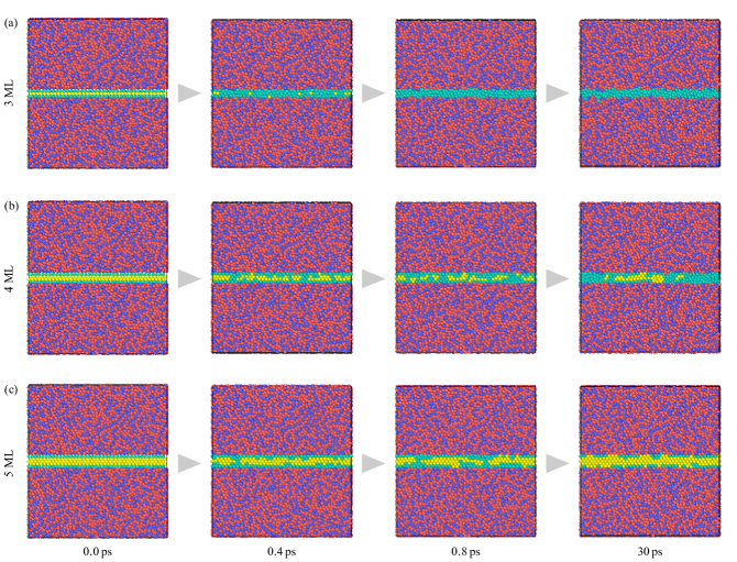
Figure 1 shows the time evolution of composite systems with different nanolayer thickness and the results of the CNA. Atoms depicted in yellow are nanolayer atoms that are fcc coordinated. On insertion, the nanolayer had a (100) surface orientation. We can see that the nanolayer with 3 ML of copper amorphizes after a short simulation time, while the copper with 5 ML thickness stays crystalline. At a thickness of 4 ML a mixed state occurs. The systems with different initial orientations show similar behavior.
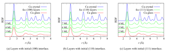
For obtaining an independent confirmation of the appearance of an amorphous and crystalline copper phase at different nanolayer thicknesses, we calculated the RDFs of the nanolayers without including the glass matrix. The results are shown in Figure 2 and compared with the RDFs of the bulk crystalline and amorphous copper reference phases. Only three layers are shown for every initial surface orientation: the thickest amorphous layer, the thinnest crystalline layer, and the layer with a mixed state. The results match the CNA. Amorphous layers show a similar RDF to the bulk amorphous copper phase, including the characteristic double peak between and . The RDFs of completely crystalline layers match the bulk fcc copper, although the signal at large gets smaller due to the finite size of the nanolayers. A mixed state is indicated by appearance of the second crystalline peak with reduced intensity. Depending on the fraction of the amorphous phase, the glass double peak starts separating into the two clearly distinct crystalline peaks (number three and four). In the system with initial (110) surface and a layer thickness of 5 ML, a small trace of crystalline phase is still detectable as indicated by a slight increase of the RDF at about , the position of the second crystalline peak.
III.2 Ward potential
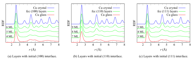
The simulations using the Ward potential show the same behavior as the simulations using the Mendelev potential. The corresponding RDFs of the copper nanolayers are shown in Figure 3. The RDFs exhibit the same characteristics, i.e., the gradual disappearance of the second crystalline peak as well as the appearance of the glass double peak with decreasing thickness. The amorphization also occurs in slightly thicker layers. For the system with an initial (100) surface, 4 ML are amorphous, and even the 5 ML system only shows a small amount of crystallization. The mixed state for the initial surfaces (110) and (111) appears at 8 ML and 4 ML, respectively. The CNA results agree with the RDFs and are comparable to Figure 1. They are therefore omitted here.
The simulations with both potentials agree that thin, initially crystalline nanolayers of copper become amorphous. Thus, we can already exclude that amorphization is a result of kinetics in the deposition process, as the layers were inserted in a crystalline state. Still, the creation of the interface may be connected with local heating, leading to a fast melt-quench process in the smaller layers. It is therefore necessary to investigate the thermodynamics of the system.
IV Model
An indication for an energetically driven amorphization is already given by the fact that even initially crystalline nanolayers undergo a phase transformation to the amorphous state. To explain the amorphization of the nanolayers and to test the hypothesis of energetically driven SSA, we propose a simple thermodynamic model. We formulate the internal energy of the composite systems. In the given ensemble, the free energy would be the appropriate thermodynamic potential, but given that the entropy term should favor the amorphization, we do not artificially increase the driving force for the amorphization, but rather underestimate it. The internal energy of a composite system with an embedded crystalline nanolayer is then
| (1) |
is the total internal energy of the bulk Cu64Zr36 glass phase, is the number of atoms in the nanolayer, is the internal energy per atom of the copper fcc crystal. Additionally, there are two interfaces, which contribute an energy of each, where is the interface area.
If the system instead contains an embedded amorphous nanolayer, the internal energy is expressed as
| (2) |
where is the per-atom internal energy of the glassy nanolayer and is the glass–glass interface energy.
Generally, it is to be expected that the internal energy of a copper crystal is lower than the internal energy of amorphous copper. As we nevertheless see amorphization of pure-metal nanolayers, the reason must lie in the interface energy. We propose that the crystal–glass interface energy is higher than the glass–glass interface energy . In that case an amorphous nanolayer must be energetically favorable if its thickness doesn’t exceed a critical value, given that differences in interface energy can compensate the excess energy of the copper glass phase. A quantitative measure is provided by the internal energy difference, here expressed as an intrinsic quantity independent of the surface area:
| (3) |
We can see that a negative value of signifies a stable crystalline nanolayer, while a positive value of signifies a stable amorphous nanolayer:
| crystalline nanolayer | ||||
Should the theory hold, we should be able to show that the critical number of atoms at is the same as observed in the simulation by CNA. To get a more descriptive quantity, the number of atoms can easily be converted to the number of monolayers or the thickness of the nanolayer , as these quantities are proportional:
The missing parameters in our model are now , , , and . Using equations 1 and 2, the internal energies of the different layer phases can be obtained from the relations
| (4) |
respectively. Alternatively, it would be conceivable to just use the internal energies of the bulk copper reference systems. The problem would be that the amorphous phase in the nanolayer is not necessarily the same as in the bulk. The bulk amorphous copper is quenched with very high cooling rates and has therefore more similarity to the melt. The amorphous copper phase in the nanolayer may exhibit different short-range order as it is allowed to relax to a low-energy state. Furthermore, the ratio of interface to volume is very high, which means that the nanolayer structure is highly influenced by interface contributions. To calculate the interface energy, the internal energy is first taken from the pure Cu64Zr36 glass sample before embedding the copper nanolayer. This allows to calculate the interface energies either by directly using equations 1 and 2, or by subtracting from the -axis intercept of the curves. Both should yield the same result. We assume here that the interface energy is constant, see Sup, , section II for proof.
IV.1 Mendelev potential
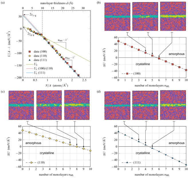
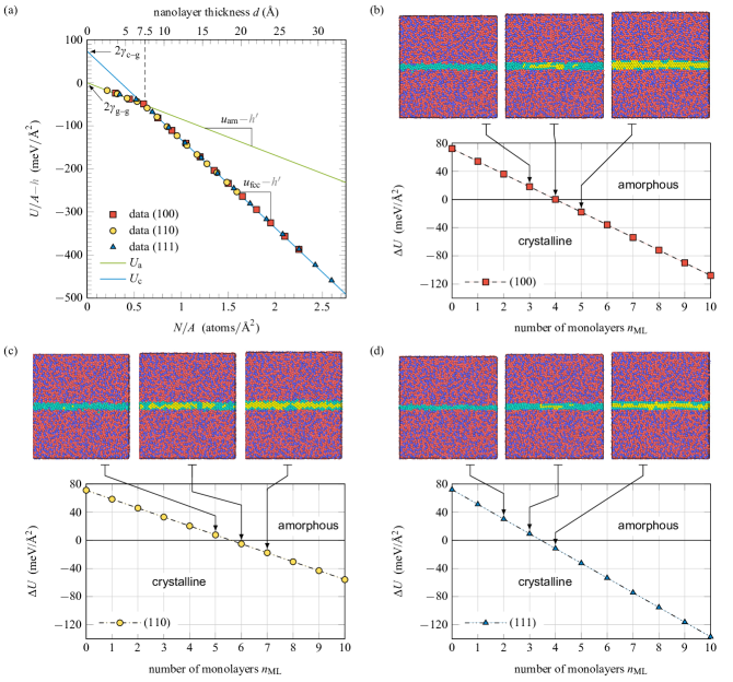
Figure 4a shows the internal energies and as a function of the number of atoms. All values are normalized to the interface area and is already subtracted. The symbols show the internal energies extracted from the MD simulation, while the lines show the linear regression. The numerical data is listed in Table 1. We note that all crystalline nanolayers have (approximately) the same interface energy in the Mendelev potential. The graph shows that the glass–glass interface energy is lower than the crystal–glass interface (in fact it is zero, which will be discussed in detail in section V), which fits the assumptions of our model. This lowered favors a glassy nanolayer up until approximately , which corresponds to a critical thickness of about
| (5) |
The thickness can only be given approximately, due to the different densities of the two phases and the rough interface. Figures 4b–d show as a function of the number of monolayers. The direct comparison reveals that the calculated energy differences and the solid-state amorphization observed by the CNA method agree very well. At the critical thickness we observe a mixed crystalline/amorphous nanolayer. The figures show that the transition is not as sharp as our model assumes, a partly crystalline layer also exists for slightly greater than zero. That is a result of omitting a description of the two-phase region in the model; entropy and the additional interfaces play a role here. Nonetheless, the critical thickness is correctly reproduced without these complications. A further comparison with the RDFs in Figure 2 leads to the same conclusions. While the good fit of the model with simulation data supports the conclusion that the SSA is due to energetic reasons, we also investigated the influence of the simulation setup on the amorphization of the nanolayers in Sup, , section III. We find that the interface creation leads to a heat spike, but that this only serves as activation energy for the SSA process. Crystalline layers with a thickness below can be produced, but are not energetically favorable.
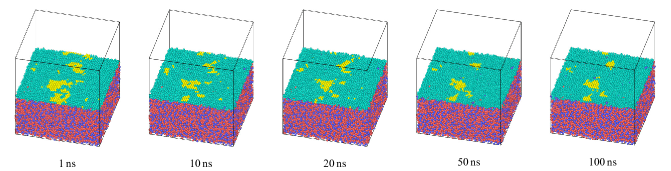
In order to verify that the amorphous phase is indeed stable over a long time scale and that this is a result of the glass–glass interface, we conducted two further simulations. In the first simulation, we simply took a composite system with a mixed crystalline/amorphous state in the copper nanolayer and let the simulation run for . If the amorphous phase is only produced by, e.g., stress in the initial system after insertion of the nanolayer, the crystalline phase should start growing again over the longer time frame. The simulation results are depicted in Figure 5 and show that the mixed state is stable, as predicted by our model.
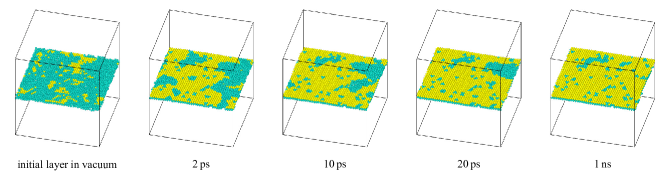
A direct proof that the solid-state amorphization is due to the presence of a glass–glass interface was obtained by removing the glass matrix. The results are shown in Figure 6. The free amorphous layer crystallizes almost immediately, as would be expected.
IV.2 Ward potential
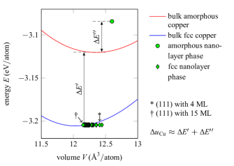
Figure 7a shows the internal energies as calculated with the Ward potential as a function of the number of atoms. All values are again normalized to the interface area and is already subtracted. The symbols show the internal energies extracted from the MD simulation, while the lines show the linear regression. In the Ward potential the (111) interface has a slightly lower interface energy than the (100) and (110) interfaces, which are approximately the same (see also Table 1). As with the Mendelev potential, the glass–glass interface energy is lower than the crystal–glass interface energy, favoring an amorphous nanolayer up to the critical thicknesses
| (6) | ||||
| (7) | ||||
| (8) |
The difference in critical thickness is a result of different for the three surface orientations. The transition thickness is higher than in the Mendelev potential despite a smaller , as the excess energy of the amorphous phase is lower. By plotting as a function of the number of monolayers, a direct comparison to CNA and RDF results is possible. Figures 7b–d show compared with snapshots from the simulation. Again, a good match between the nanolayer phases shown in the snapshots and the predicted critical thickness is visible. For the same reasons as stated earlier, a mixed state occurs.
All in all, the results using both potentials agree qualitatively and support our thermodynamic model. Therefore, a purely kinetic reason for the amorphous nanolayers can be ruled out and an energetic picture of solid-state amorphization can be supported.
V Structure and Energy
V.1 Mendelev
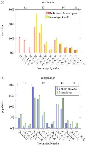
We compared the energy of the amorphous nanolayer copper phase with the reference bulk amorphous copper phase. The energy–volume curve in Figure 8 shows that the nanolayer phase is energetically higher than the bulk phase. Additionally, an expansion of the crystalline layer at low thicknesses is visible, possibly due to interface stress. Both the peculiarity of the zero glass–glass interface energy, as well as the higher excess energy of the amorphous phase can be linked to the structure of the phase. Figure 9a shows the Voronoï statistics of those copper atoms in the nanolayer, that are only surrounded by other copper atoms. This allows a comparison to bulk amorphous copper: in contrast to the bulk phase, the nanolayer phase contains no twelve-fold coordinated atoms. This higher energy structure is stabilized by the interface, as shown in Figure 9b: the Voronoï statistics of the whole nanolayer (including copper atoms that have zirconium neighbors) are very similar to the bulk Cu64Zr36. This reduces the interface energy to almost zero.
V.2 Ward
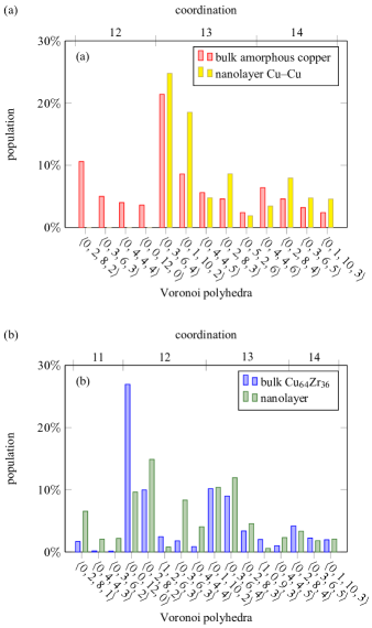
In the Ward potential the amorphous nanolayer also features a structure with different energy than the bulk amorphous copper ( for the reference system, for the amorphous nanolayer). The explanation can again be found in the Voronoï statistics of nanolayer copper atoms surrounded completely by other copper atoms: Figure 10a shows that the twelve-fold coordinated atoms are missing again. The comparison of the Voronoï statistics of the whole nanolayer, though, show a difference to the Cu64Zr36 MG, especially concerning the , , and polyhedra (Figure 10b). This leads to a small but non-zero glass–glass interface energy.
| Potential | Initial interface | ||||||||
|---|---|---|---|---|---|---|---|---|---|
| () | () | () | (Å) | ||||||
| Mendelev | (100) | ||||||||
| (110) | |||||||||
| (111) | |||||||||
| Ward | (100) | ||||||||
| (110) | |||||||||
| (111) | |||||||||
VI Conclusions
Using MD simulations, we observed the amorphization of elemental copper nanolayers embedded in a Cu64Zr36 metallic glass if the layer thickness stays below a critical value. This is in accordance with experimental results, which report thin amorphous iron nanolayers embedded in Co75Fe12B13 Ghafari et al. (2012). We could show that the amorphization is not a kinetic effect due to deposition, as our simulations start from a crystalline state. Rather, the glass–glass interface energy is significantly lower than the crystal–glass interface energy, which stabilizes the amorphous copper phase. This solid-state amorphization is similar to the case at heterogeneous crystal interfaces, except that in our case the reduced glass–glass interface energy is sufficient to induce amorphization. At a critical layer thickness, which is on the order of a nanometer, a mixed crystalline/amorphous state appears. This state is also stable over longer times, which further supports the picture of solid-state amorphization: if the amorphous state is only a result of stresses in the initial setup, the crystallites in the layer would grow again with time. They instead keep their size. Analysis of the amorphous structure in the nanolayer further confirms that the interface energy is a dominating factor in the structure of thin nanolayers: if it can be reduced, the amorphous layer can even be driven into a state with a higher bulk energy than a quenched melt. Technological applications for glass–glass composite systems have already been proposed in the realm of magnetic tunnel junctions Gao et al. (2009); Ghafari et al. (2012) and could benefit from further research into different multilayer systems.
Acknowledgements.
We would like to thank Mohammad Ghafari for many helpful discussions. The authors gratefully acknowledge financial support by the Deutsche Forschungsgemeinschaft (DFG) through project grant no. AL 578/13-1, as well as a DAAD-PPP travel grant to Finland. We also acknowledge the computing time granted by the John von Neumann Institute for Computing (NIC) and provided on the supercomputer JUROPA at Jülich Supercomputing Centre (JSC). Computation time was also made available by the State of Hesse on the Lichtenberg Cluster at TU Darmstadt.References
- Klement et al. (1960) W. Klement, R. H. Willens, and P. Duwez, Nature 187, 869 (1960).
- Inoue et al. (1989) A. Inoue, T. Zhang, and T. Masumoto, Mater. Trans. JIM 30, 965 (1989).
- Inoue et al. (1990) A. Inoue, T. Zhang, and T. Masumoto, Mater. Trans. JIM 31, 177 (1990).
- Averback and Diaz de la Rubia (1997) R. S. Averback and T. Diaz de la Rubia, in Solid State Physics, Solid State Physics, Vol. 51, edited by H. Ehrenreich and F. Spaepen (Academic Press, 1997) pp. 281–402.
- Kazmerski (1980) L. L. Kazmerski, ed., Polycrystalline and amorphous thin films and devices (Academic Press, 1980).
- Yoshida and Fujita (1972) N. Yoshida and F. E. Fujita, J. Phys. F Met. Phys. 2, 1009 (1972).
- Bialas and Heneka (1994) H. Bialas and K. Heneka, Vacuum 45, 79 (1994).
- Møller and Guo (1991) P. J. Møller and Q. Guo, Thin Solid Films 201, 267 (1991).
- Dehm et al. (1995) G. Dehm, M. Rühle, G. Ding, and R. Raj, Philos. Mag. B 71, 1111 (1995).
- Koziol et al. (1987) C. Koziol, G. Lilienkamp, and E. Bauer, Appl. Phys. Lett. 51, 901 (1987).
- Keblinski et al. (1999) P. Keblinski, D. Wolf, S. R. Phillpot, and H. Gleiter, Scr. Mater. 41, 631 (1999).
- Wolf et al. (1995) D. Wolf, J. Wang, S. R. Phillpot, and H. Gleiter, Phys. Lett. A 205, 274 (1995).
- Zheng and Li (2007) G.-P. Zheng and M. Li, Acta Mater. 55, 5464 (2007).
- Baletto and Ferrando (2005) F. Baletto and R. Ferrando, Rev. Mod. Phys. 77, 371 (2005).
- Schwarz and Johnson (1983) R. B. Schwarz and W. L. Johnson, Phys. Rev. Lett. 51, 415 (1983).
- Benedictus et al. (1996) R. Benedictus, A. Böttger, and E. J. Mittemeijer, Phys. Rev. B 54, 9109 (1996).
- Benedictus et al. (1998) R. Benedictus, K. Han, C. Træholt, A. Böttger, and E. J. Mittemeijer, Acta Mater. 46, 5491 (1998).
- Cantwell et al. (2014) P. R. Cantwell, M. Tang, S. J. Dillon, J. Luo, G. S. Rohrer, and M. P. Harmer, Acta Mater. 62, 1 (2014).
- Landes et al. (1991) J. Landes, C. Sauer, B. Kabius, and W. Zinn, Phys. Rev. B 44, 8342 (1991).
- Handschuh et al. (1993) S. Handschuh, J. Landes, U. Köbler, C. Sauer, G. Kisters, A. Fuss, and W. Zinn, J. Magn. Magn. Mater. 119, 254 (1993).
- Herr (2000) U. Herr, Contemp. Phys. 41, 93 (2000).
- Ghafari et al. (2012) M. Ghafari, H. Hahn, R. A. Brand, R. Mattheis, Y. Yoda, S. Kohara, R. Kruk, and S. Kamali, Appl. Phys. Lett. 100, 203108 (2012).
- Plimpton (1995) S. Plimpton, J. Comp. Phys. 117, 1 (1995), http://lammps.sandia.gov/.
- Mendelev et al. (2009) M. I. Mendelev, M. J. Kramer, R. T. Ott, D. J. Sordelet, D. Yagodin, and P. Popel, Philos. Mag. 89, 967 (2009).
- Zhou et al. (2004) X. W. Zhou, R. A. Johnson, and H. N. G. Wadley, Phys. Rev. B 69, 144113 (2004).
- (26) L. Ward, A. Agrawal, K. M. Flores, and W. Windl, arXiv:1209.0619 [cond-mat.mtrl-sci] (2012).
- Ritter et al. (2011) Y. Ritter, D. Şopu, H. Gleiter, and K. Albe, Acta Mater. 59, 6588 (2011).
- Cheng et al. (2008) Y. Q. Cheng, A. J. Cao, H. W. Sheng, and E. Ma, Acta Mater. 56, 5263 (2008).
- (29) See Supplemental Material appended to this paper for a discussion of additional details of the simulation setup.
- Honeycutt and Andersen (1987) J. D. Honeycutt and H. C. Andersen, J. Phys. Chem. 91, 4950 (1987).
- Stukowski (2012) A. Stukowski, Model. Simul. Mater. Sc. 20, 045021 (2012).
- Stukowski (2010) A. Stukowski, Model. Simul. Mater. Sc. 18, 015012 (2010), http://ovito.org/.
- Voronoï (1908a) G. Voronoï, J. Reine Angew. Math. 133, 97 (1908a).
- Voronoï (1908b) G. Voronoï, J. Reine Angew. Math. 134, 198 (1908b).
- Voronoï (1909) G. Voronoï, J. Reine Angew. Math. 136, 67 (1909).
- Brostow et al. (1998) W. Brostow, M. Chybicki, R. Laskowski, and J. Rybicki, Phys. Rev. B 57, 13448 (1998).
- Gao et al. (2009) L. Gao, X. Jiang, S.-H. Yang, P. M. Rice, T. Topuria, and S. S. P. Parkin, Phys. Rev. Lett. 102, 247205 (2009).
See pages 1 of supplemental-1.pdf See pages 1 of supplemental-2.pdf See pages 1 of supplemental-3-small.pdf See pages 1 of supplemental-4-small.pdf See pages 1 of supplemental-5.pdf