Anisotropic magneto-capacitance in ferromagnetic-plate capacitors
Abstract
The capacitance of a parallel plate capacitor can depend on applied magnetic field. Previous studies have identified capacitance changes induced via classical Lorentz force or spin-dependent Zeeman effects. Here we measure a magnetization direction dependent capacitance in parallel-plate capacitors where one plate is a ferromagnetic semiconductor, gallium manganese arsenide. This anisotropic magneto-capacitance is due to the anisotropy in the density of states dependent on the magnetization through the strong spin-orbit interaction.
Capacitance, the ability of a body to retain charge is defined by the relation , the ratio of the change in electrostatic potential to the amount of charge added. In a simple parallel plate capacitor one normally calculates this capacitance through the change in electrostatic potential by integrating the electric field due to charges on the surface of two metallic plates over the separating distance . However, corrections to this electrostatic picture can be important, and other contributions to the change in potential when additional charge is added must be taken into account. It is often helpful to reformulate these corrections as effective series capacitances in series with a geometrical capacitance expected from the classical picture Stern (1972); Smith et al. (1985); Büttiker et al. (1993). In particular, the effect of change in chemical potential due to the finite density of states can be important in low dimensional systems. This has been exploited for example in two-dimensional electron gases where the additional chemical contribution to the potential, the electron compressibility, allows probing of Landau levels in the density of states in the quantum Hall regime Smith et al. (1985).
In this Letter, we exploit this kind of capacitance correction to demonstrate an anisotropic magneto-capacitance (AMC). This is analogous to anisotropic magneto-resistance (AMR) Thomson (1856), an important technology in magnetic field sensing applications Thompson et al. (1975) and of a similarly relativistic magnetic origin, but in this different fundamental electrical circuit element.
In general, magnetic effects on transport properties such as AMR can be ascribed to three different categories: ordinary (orbital), due to the Lorentz force; spin-dependent, due to splitting of spin sub-bands through ferromagnetism or the Zeeman effect; and extraordinary, relativistic in origin through the spin-orbit interaction. Some well known examples of these effects in resistance are Lorentz magneto-resistance, giant magneto-resistance (GMR) Baibich et al. (1988), and AMR McGuire and Potter (1975) respectively. Classifying magneto-capacitance along similar lines, both ordinary and spin-dependent effects have been observed previously. Changes in capacitance as a function of in-plane magnetic field have been measured in two-dimensional electron gases and attributed to combined Lorentz force and quantum confinement effects Hampton et al. (1995); Jungwirth and Smrčka (1995); spin dependent effects have been considered theoretically Zhang (1999), and experimentally measured due to the Zeeman splitting in Pd plate capacitors McCarthy et al. (2003) and in magnetic tunnel junctions several measurements have shown changes in capacitance as a function of relative magnetization orientation Kaiju et al. (2002); Padhan et al. (2007); Chang et al. (2010). The demonstration in this paper is of the third class, an anisotropic magneto-capacitance whose origin is in the spin-orbit interaction.
It is also worth noting the connection of a modulation in capacitance to that of a different quantity, the chemical potential. Changes in chemical potential can be measured by exploiting the capacitance of a structure and measuring the rearrangement of charge to maintain equilibrium. By contrast, a change in capacitance does not change the equilibrium charge distribution, but the variation of charge with respect to voltage (the definition of capacitance). While magnetically induced changes in chemical potential have been measured experimentally in single electron transistor devices as spin-dependent magneto-coulomb oscillations Ono et al. (1997, 1998), and spin-orbit interaction induced coulomb-blockade AMR Wunderlich et al. (2006); Schlapps et al. (2009); Bernand-Mantel et al. (2009); Ciccarelli et al. (2012), anisotropies in the capacitance were not observed or considered. There, the capacitance of the devices was small and remains constant so that the sensitivity is to the chemical potential; if a change in the capacitance were observed in coulomb blockaded transport it would have appeared in the period of the oscillating conductivity, rather than the observed shift.
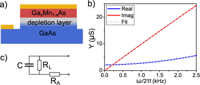
The system in which we chose to demonstrate AMC is the ferromagnetic semiconductor (Ga,Mn)As Ohno et al. (1996). This material is known to exhibit anisotropy in the density of states Jungwirth et al. (2006), as is experimentally demonstrated by the large tunneling anisotropic magneto-resistance (TAMR) Gould et al. (2004). The 25 nm (Ga,Mn)As layer is grown by standard low temperature molecular beam epitaxy, with manganese concentration of , on a 1.5 m -GaAs layer (nominal doping cm-3) with a contact layer cm-3 below. The depletion layer of this p-n junction is used as the dielectric of the capacitor. Wafers are fabricated into large-area planar structures using optical lithography and wet chemical etching and contacts to the (Ga,Mn)As and n+-GaAs layers are made through thermal evaporation of Cr/Au and AuGeNi respectively (fig. 1(a)). The (Ga,Mn)As is as-grown with around 42 K.
Experiments are performed in a 3-axis vector magnet cryostat. A lock-in amplifier is used to measure the quadrature components of the current with a small applied voltage excitation across the capacitor as a function of excitation frequency from dc to 2.5 kHz. An example of such a measurement is shown in fig. 1(b). A linear dependence in the imaginary (out-of-phase) part of the admittance on excitation frequency indicates the dominance of capacitance in this device. In addition, in the real (in-phase) admittance there is a offset due to a parallel ohmic leakage resistance through the dielectric layer and a quadratic part due to this leakage and the resistance of the leads. To extract the capacitance the complex admittance is fitted to a simple lumped element circuit model (fig. 1(c)) which includes the capacitance , leakage resistance , and an access resistance in the -GaAs contact layer, which gives:
| (1) |
The prefactor has only a small effect as is small and we work at low frequencies. The quality of the fit is excellent as can be seen from the dashed lines in fig 1(b). This measurement is repeated as a function of magnetic field direction in order to rotate the magnetization in the (Ga,Mn)As.
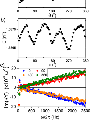
In fig. 2 the capacitance is plotted as a function of in-plane (a) and out-of-plane (b) magnetic field orientation of magnitude 0.5 T. There is a clear cubic in-plane symmetry, and uniaxial out-of-plane symmetry to the change in capacitance. This is the symmetry that might be expected due to the bulk cubic crystal symmetry in the plane and uniaxial out-of-plane anisotropy due to the compressive strain on the (Ga,Mn)As epilayer from the GaAs substrate.. The size of the modulation of the capacitance is out-of-plane and in-plane. This small ratio could in principle be strengthened by increasing the geometrical capacitance, as will be discussed in the analysis. For these rotation experiments, effectively no change in the leakage or access resistance is measured within experimental accuracy. To conclusively demonstrate that it is a change in capacitance which we are measuring, we also plot in fig. 2(c) the difference in the imaginary part of the admittance from the mean for four directions of the magnetization with respect to the plane. As expected, these are straight lines as a function of frequency given by .
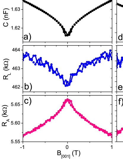
The capacitance is also measured as a function of magnetic field strength (fig. 3). Here, hysteresis is observed for in-plane field directions evidencing the magnetic origin of this effect. An isotropic linear magneto-capacitance is also observed extending to high magnetic fields where the magnetisation is already saturated. A similiar effect has been seen in (Ga,Mn)As in CBAMR, and was understood through two mechanism Ciccarelli et al. (2012). Firstly the field dependence of a small amount of unsaturated manganese moments, and secondly the Zeeman splitting of the bands. While we are sensitive to a different quantity in our experiments, both these mechanisms likely play a role in the measured linear magneto-capacitance, as well as isotropic magneto-capacitance contributions in the non-magnetic n-GaAs Tongay et al. (2009). In addition, the access and leakage resistance both show separately a small magneto-resistance. We note here that while it has been shown that a series capacitance can mean that any magneto-resistance appears as a spurious measured magneto-capacitance Catalan (2006), this can be excluded in our devices. In order for the observed magneto-resistance to appear in the measured capacitance, it would require that the series capacitance be in excess of 100 nF, much greater than can be reasonable expected given the geometry of our devices.
There are two possible contributions to the AMC that we observe. One is related to the modulation of the density of states and the other to that of the chemical potential. The latter is specific to the p-n junction structure of these devices, but both are extra-ordinary magneto-capacitance effects and we attempt to differentiate the two by treating them separately.
The effect of the density of states on capacitance is often evident in low dimensional systems where the density of states is small and the additional change in potential is inversely proportional to the density of states. In 2D systems, for example, this is often reformulated as an additional capacitance per area , for density of states , in series with the electro-static geometric capacitance. This is termed the quantum capacitance Iafrate et al. (1995) in the zero temperature limit and electron compressibility Eisenstein et al. (1994) when the density of states is smeared out at finite temperature. The effect has important consequences in capacitors formed from 2D systems such as semiconductor hetereostructures Smith et al. (1986) and graphene Ponomarenko et al. (2010), 1D systems such as carbon nanotubes Ilani et al. (2006) and 0D systems such as quantum dots Hansen et al. (1989); Ashoori et al. (1992), where changes in the density of states have been measured through the effect on the measured capacitance. These measurements were possible through the ability of some external parameter to change the density of states, which then allows the separation of the contributions to capacitance which would be otherwise indistinguishable. In our experiment, this handle is provided by the direction of the magnetization with respect to the crystallographic axes.
In 3D systems, the density of states is generally much larger and the corrections to the capacitance can often be neglected. In addition, the separation of the plates becomes an ill-defined quantity once the finite screening length in the plate is taken into account Büttiker (1993). The chemical potential contribution to the capacitance then depends on how the charge is distributed in the contact. This distribution of charge is itself defined by the competition between the electrostatic and potential energies. However, based on the Thomas-Fermi screening length one can formulate an effective series capacitance formulated in 3D Büttiker (1993), with an equivalent dependence on the density of states Kopp and Mannhart (2009) similar to that for the electron compressibility, the kinetic capacitance.
| (2) |
Where is the density of states and is the effective dielectric constant of the contact material, which we take to be that of bulk GaAs. To asses whether the change in resistance can be explained by the anisotropy of the density of states in the ferromagnet, we use an approximated value of the total density of states to obtain an estimate of the corresponding change which would be needed to give the observed capacitance modulation. Taking J-1m-3 Neumaier et al. (2009), we estimate 50 fFm-2. The change in the total capacitance of the device can be related to the change in the kinetic capacitance by
| (3) |
It can be seen from this equation that increasing the ratio of total to kinetic capacitance would increase the size of the modulation. The total capacitance per area of our device is 2 fFm-2. From these values a 5% change in the density of states would be needed to explain the 0.1% change in capacitance measured for the out-of-plane field rotation, a value which is reasonable in these as-grown material.
We now consider the effect of the anisotropy in chemical potential. Because our capacitors are p-n junctions, any change in the difference in chemical potential across the device would change the width of the depletion layer in the -GaAs and thus modulate the capacitance in a different way. To ascertain whether this is possible, we measure the capacitance of our devices as a function of dc bias voltage. We can then compare the voltage which is needed to obtain a comparable shift in the capacitance to that expected from the anisotropy of the chemical potential (fig. 4). To obtain the same change in capacitance we observe for the out-of-plane rotation the change in chemical potential would need to be 5 mV. This value is much larger than that measured in (Ga,Mn)As through CBAMR in both disordered planar devices Wunderlich et al. (2006) and aluminum single electron transistors Ciccarelli et al. (2012). In this case we can largely assign the observed AMC to a density of states effect.

As the density of states AMC is not reliant on the p-n junction structure we have used, it should also be observable more generally in normal dielectric capacitors with ferromagnetic, or indeed antiferromagnetic contacts with strong spin-orbit coupling. Conditions are more favorable in materials with low absolute density of states, as this reduces the total kinetic capacitance and therefore makes it easier to achieve a comparable geometric capacitance with typical thicknesses and strengths of dielectric materials. In this light, antiferromagnetic semiconductors would be a prime candidate for room temperature devices with large effects. In addition, the magneto-capacitance observed by McCarthy et al. McCarthy et al. (2003) in metal plate capacitors provides a hint that AMC could be observed in metallic ferromagnets, where a possible candidate might be CoPt whose strong spin-orbit interaction, and the resulting considerable density of states anisotropies, facilitates a large TAMR Shick et al. (2006); Park et al. (2008).
We would like to acknowledge support from Hitachi Cambridge Laboratory, the EU European Research Council (ERC) Advanced Grant No. 268066, the Ministry of Education of the Czech Republic Grant No.LM2011026, and the Grant Agency of the Czech Republic Grant No. 14-37427G.
References
- Stern (1972) F. Stern, Physical Review B 5, 4891 (1972).
- Smith et al. (1985) T. P. Smith, B. B. Goldberg, P. J. Stiles, and M. Heiblum, Physical Review B 32, 2696 (1985).
- Büttiker et al. (1993) M. Büttiker, H. Thomas, and A. Prêtre, Physics Letters A 180, 364 (1993).
- Thomson (1856) W. Thomson, Proceedings of the Royal Society of London 8, 546 (1856).
- Thompson et al. (1975) D. A. Thompson, L. Romankiw, and A. Mayadas, IEEE Transactions on Magnetics 11, 1039 (1975).
- Baibich et al. (1988) M. N. Baibich, J. M. Broto, A. Fert, F. Nguyen Van Dau, F. Petroff, P. Etienne, G. Creuzet, A. Friederich, and J. Chazelas, Physical Review Letters 61, 2472 (1988).
- McGuire and Potter (1975) T. McGuire and R. Potter, IEEE Transactions on Magnetics 11, 1018 (1975).
- Hampton et al. (1995) J. Hampton, J. Eisenstein, L. Pfeiffer, and K. West, Solid State Communications 94, 559 (1995).
- Jungwirth and Smrčka (1995) T. Jungwirth and L. Smrčka, Physical Review B 51, 10181 (1995).
- Zhang (1999) S. Zhang, Physical Review Letters 83, 640 (1999).
- McCarthy et al. (2003) K. T. McCarthy, A. F. Hebard, and S. B. Arnason, Physical Review Letters 90, 117201 (2003).
- Kaiju et al. (2002) H. Kaiju, S. Fujita, T. Morozumi, and K. Shiiki, Journal of Applied Physics 91, 7430 (2002).
- Padhan et al. (2007) P. Padhan, P. LeClair, A. Gupta, K. Tsunekawa, and D. D. Djayaprawira, Applied Physics Letters 90, 142105 (2007).
- Chang et al. (2010) Y.-M. Chang, K.-S. Li, H. Huang, M.-J. Tung, S.-Y. Tong, and M.-T. Lin, Journal of Applied Physics 107, 093904 (2010).
- Ono et al. (1997) K. Ono, H. Shimada, and Y. Ootuka, Journal of the Physical Society of Japan 66, 1261 (1997).
- Ono et al. (1998) K. Ono, H. Shimada, and Y. Ootuka, Solid-State Electronics 42, 1407 (1998).
- Wunderlich et al. (2006) J. Wunderlich, T. Jungwirth, B. Kaestner, A. C. Irvine, A. B. Shick, N. Stone, K.-Y. Wang, U. Rana, A. D. Giddings, C. T. Foxon, et al., Physical Review Letters 97, 077201 (2006).
- Schlapps et al. (2009) M. Schlapps, T. Lermer, S. Geissler, D. Neumaier, J. Sadowski, D. Schuh, W. Wegscheider, and D. Weiss, Physical Review B 80, 125330 (2009).
- Bernand-Mantel et al. (2009) A. Bernand-Mantel, P. Seneor, K. Bouzehouane, S. Fusil, C. Deranlot, F. Petroff, and A. Fert, Nature Physics 5, 920 (2009).
- Ciccarelli et al. (2012) C. Ciccarelli, L. P. Zârbo, A. C. Irvine, R. P. Campion, B. L. Gallagher, J. Wunderlich, T. Jungwirth, and A. J. Ferguson, Applied Physics Letters 101, 122411 (2012).
- Ohno et al. (1996) H. Ohno, A. Shen, F. Matsukura, A. Oiwa, A. Endo, S. Katsumoto, and Y. Iye, Applied Physics Letters 69, 363 (1996).
- Jungwirth et al. (2006) T. Jungwirth, J. Sinova, J. Mašek, J. Kučera, and A. H. MacDonald, Reviews of Modern Physics 78, 809 (2006).
- Gould et al. (2004) C. Gould, C. Rüster, T. Jungwirth, E. Girgis, G. M. Schott, R. Giraud, K. Brunner, G. Schmidt, and L. W. Molenkamp, Physical Review Letters 93, 117203 (2004).
- Tongay et al. (2009) S. Tongay, A. F. Hebard, Y. Hikita, and H. Y. Hwang, Physical Review B 80, 205324 (2009).
- Catalan (2006) G. Catalan, Applied Physics Letters 88, 102902 (2006), ISSN 0003-6951, 1077-3118.
- Iafrate et al. (1995) G. J. Iafrate, K. Hess, J. B. Krieger, and M. Macucci, Physical Review B 52, 10737 (1995).
- Eisenstein et al. (1994) J. P. Eisenstein, L. N. Pfeiffer, and K. W. West, Physical Review B 50, 1760 (1994).
- Smith et al. (1986) T. P. Smith, W. I. Wang, and P. J. Stiles, Physical Review B 34, 2995 (1986).
- Ponomarenko et al. (2010) L. A. Ponomarenko, R. Yang, R. V. Gorbachev, P. Blake, A. S. Mayorov, K. S. Novoselov, M. I. Katsnelson, and A. K. Geim, Physical Review Letters 105, 136801 (2010).
- Ilani et al. (2006) S. Ilani, L. a. K. Donev, M. Kindermann, and P. L. McEuen, Nature Physics 2, 687 (2006).
- Hansen et al. (1989) W. Hansen, T. P. Smith, K. Y. Lee, J. A. Brum, C. M. Knoedler, J. M. Hong, and D. P. Kern, Physical Review Letters 62, 2168 (1989).
- Ashoori et al. (1992) R. C. Ashoori, H. L. Stormer, J. S. Weiner, L. N. Pfeiffer, S. J. Pearton, K. W. Baldwin, and K. W. West, Physical Review Letters 68, 3088 (1992).
- Büttiker (1993) M. Büttiker, Journal of Physics: Condensed Matter 5, 9361 (1993).
- Kopp and Mannhart (2009) T. Kopp and J. Mannhart, Journal of Applied Physics 106, 064504 (2009).
- Neumaier et al. (2009) D. Neumaier, M. Turek, U. Wurstbauer, A. Vogl, M. Utz, W. Wegscheider, and D. Weiss, Physical Review Letters 103, 087203 (2009).
- Shick et al. (2006) A. B. Shick, F. Máca, J. Mašek, and T. Jungwirth, Physical Review B 73, 024418 (2006).
- Park et al. (2008) B. G. Park, J. Wunderlich, D. A. Williams, S. J. Joo, K. Y. Jung, K. H. Shin, K. Olejník, A. B. Shick, and T. Jungwirth, Physical Review Letters 100, 087204 (2008).