Tunable asymmetric transmission of THz wave through a graphene planar chiral structure
Abstract
In this letter, we show that asymmetric transmission of circularly polarized waves through a nanostructured planar chiral graphene film can be observed in terahertz range. The asymmetric transmission effect of monatomic layer graphene closely resembles that of metallic planar chiral nanostructures which has previously been demonstrated. And the relative enantiomeric difference in the total transmission varies with the change of graphene’s Fermi level. The plasmonic excitation in the graphene nanostructure is the enantiometically sensitive which is asymmetric for opposite propagating directions. This phenomenon will deepen our understanding of light-matter interactions in planar chiral structures and may find applications in polarization-sensitive devices, sensors, detectors and other areas.
1College of Optoelectronic Science and Engineering, National University of Defense Technology, Changsha 410073, China
2State Key Laboratory of High Performance Computing, National University of Defense Technology, Changsha 410073, China
∗Corresponding author: jfzhang85@nudt.edu.cn
(250.5403) Plasmonics;(160.1190) Anisotropic materials;(310.6628) Subwavelength structures, nanostructures.
During the past several years the research on chiral metamaterials have revealed several new electromagnetic phenomena, such as circular dichroism [1, 2, 3] and elliptical dichroism [4] of planar chiral metamaterials, unidirectional or asymmetric transmission of linearly polarized waves in three-dimension chiral metamaterials [5, 6, 7, 8, 9, 10, 11, 12] or circularly polarized waves in planar chiral structures [13, 14, 15, 16]. The intriguing optical properties of metallic chiral structures are of great interests both for theoretical research and for practical applications [17, 18, 19]. In 2006, it was reported that the first experimental observation of a polarization sensitive transmission effect which is asymmetric with respect to the direction of wave propagation [13]. The reported asymmetric phenomenon requires simultaneous presence of planar chirality and anisotropy in the structure which is lossy [14]. This new asymmetric transmission effect is different from the symmetric effect analogous to conventional optical activity [20, 21, 22, 23, 24] and gyrotropy in 3D-chiral media [25, 26]. Moreover, its asymmetric transmission behaviour is fundamentally distinct from that with non-reciprocal media [27] or three-dimensional helical structures [28, 29]. And it has been associated the excitation of enantiomerically sensitive plasmons in the metal nanostructures.
Recently, graphene has raised as a powerful plasmonic material. A monolayer of doped graphene can resemble a thin metal film and support the excitation of surface plasmons in mid-infrared and terahertz (THz) ranges while it is only atomically thick. The exploration of plasmons in graphene nanostructures has leads to the proposition and demonstration of a variety of devices such as tunable polarizers [30, 31] , metamaterials [32] and perfect absorbers [33, 34]. Here we show that tunable asymmetric transmission of circularly polarized light can be realized in the THz range with a monolayer graphene patterned with arrays of G-shaped micro-holes which forms a truly planar structure.
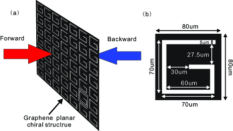
Figure 1 shows the schematic illustration of the graphene planar chiral structure. The graphene is patterned with arrays of G-shape holes with dimensions in the micro-meter scale. One circularly polarized (left or right circular polarization) THz wave normally impinges on the graphene film from forward and backward direction, respectively (see figure 1(a)). Figure 1(b) shows a unit cell of the graphene planar chiral structure with geometric parameters. The black area is graphene and the white area is the removed pattern. The period of the structure is , which ensures that the structure does not diffract at the studied spectral range at normal incidence. The side length and width of G-shaped holes are and , respectively
Using a fully three-dimensional finite element numerical simulation method(in Comsol Multi-Physics), with periodic boundary conditions applied to the unit cell, we studied the transmission, reflection and absorption properties of the graphene planar chiral structure in the wavelength range for the case of circularly polarized light at normal incidence. The Fermi level of graphene ranges from 0.6 eV to 1.2 eV. The optical conductivity of graphene can be derived within the random-phase approximation (RPA) in the local limit [35, 36]
| (1) |
where is the Boltzmann constant, is the temperature, is the frequency of light, is the carrier relaxation lifetime, and is the Fermi energy. The first term in Eq. (1) corresponds to intra-band transitions and the second term is attributed to inter-band transitions. Equation (1) reduces to the Drude model if we neglect both inter-band transitions and the effect of temperature ()
| (2) |
where depends on the concentration of charged doping and , where is the Fermi velocity and is the dc mobility. Here we use a moderate measured mobility .
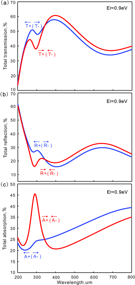
It should be noted that for a certain type of circularly polarized light (i.e., right or left circularly polarized), the transmitted light may change the polarization state and contains both light and left circularly polarized light. The transmission can be presented in terms of a circular transmission matrix , whose indexes ”+” and ”-” denote right (RCP) and left (LCP) circular polarizations, respectively. Matrix will be denoted as for a wave incident on the front side of the structure, while the arrow will be in opposite direction corresponds to the wave incident from the opposite direction. The transmission matrix will be denoted as . For instance, the data presented in figure 2a illustrates . For incident RCP wave, the total transmission in the backward direction is given by , while in the opposite direction . Figure 2a shows the total transmission of right circularly polarized wave (defined as the electric vector of the wave coming toward you appears to be rotating counterclockwise) incident from forward and backward directions when the Fermi level of graphene is 0.9 eV. It shows asymmetry depending on the the direction of propagation. According to Ref. [14], , while . It means the difference in the total transmission depends on the fact of the asymmetric conversion of transmission for a circular polarized wave into one of opposite handedness. And the total reflection (R) and absorption (A) shows similar asymmetry, as shown in figure 2b and 2c. The results are similar to those of metallic planar chiral metamaterials [14].
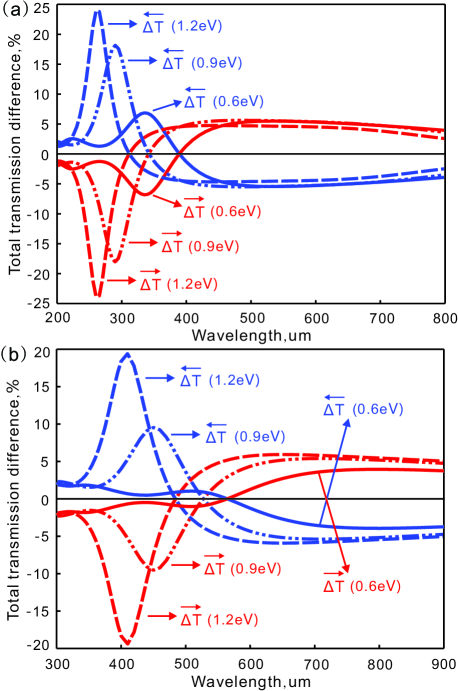
Figure 3 shows the relative enantiomeric difference in the total transmission without a substrate and with a substrate of quartz, respectively, for the different Fermi levels. The relative enantiomeric difference in the total transmission is defined as and . It displays a resonant nature and varies with the Fermi level of graphene. Figure 3a shows the situation for a free-standing graphene as in Figure 2. When Fermi levels are 0.6 eV and 0.9 eV, it reaches its maximum value of about 0.068 and 0.18 at the resonant wavelength of and , respectively. As the Fermi level increases to 1.2 eV, the maximum value increases to 0.24 at the resonant wavelength of about .
Figure 3b shows the relative enantiomeric difference in the total transmission obtained in the same graphene planar chiral structure supported on a quartz substrate. The substrate is assumed to be semi-infinite. In our studied Thz range, it can be treated as a transparent material with the refractive index of 1.96 from Ref. [37]. With the presence of a substrate, the plasmonic resonances of the graphene film redshifts to longer wavelengthes. The results closely resemble those without a substrate presented even thought the relative enantiomeric difference is slightly smaller at the resonances. When Fermi level is 0.6 eV, the difference is unconspicuous. As the Fermi level increases to 1.2 eV, it reaches the maximum value of 0.194 at about . Moreover, The sign of is changed upon reversal of the propagation direction.
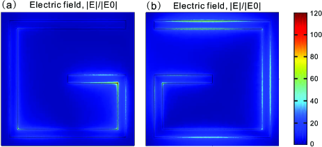
Similar to metallic planar chiral structures that have been previously studied, the asymmetric transmission here is attributed to the excitation of enantiomerically sensitive plasmons in the graphene structure. Figure 4 shows normalized electric field intensity maps at the resonance wavelength when the LCP wave propagates in opposite directions. The tFermi level of graphene is 0.9 eV. The figure reveals the strength and location of the plasmonic excitations in the plane of the structure and exhibits striking difference for the THz wave incident from forward and backward directions.
In summary, we have numerically shown the asymmetric transmission effect in graphene planar chiral structures and the results are closely resemble those in metal planar chiral nanostructures. The monatomic layer graphene can be treated as the thinnest material that can be realized and it will deepen our understanding light-matter interactions in planar chiral structures. The relative enantiomeric difference is tunable with the change of Fermi level. The plasmon excitation in the graphene planar chiral structure is enantiometically sensitive and depends on propagating directions of circularly polarized light. The plasmonic dissipation in the graphene structure is also asymmetric for opposite propagating directions. This phenomenon may find applications in polarization-sensitive devices, sensors, detectors and other areas. For example, the enantiometically sensitive excitation of graphene plasmons can be used to detect the circularly polarized light which has significant applications in chemistry and biology.
Acknowledgment. This work was supported by National Natural Science Foundation of China [Grant Nos. 11304389 and 61177051] and Ministry of Science and Technology of China [Grant No. 2012CB933501].
References
- [1] M. Decker, M. Klein, M. Wegener, and S. Linden, Optics letters 32, 856 (2007).
- [2] D.-H. Kwon, P. L. Werner, and D. H. Werner, Optics express 16, 11802 (2008).
- [3] V. Valev, N. Smisdom, A. Silhanek, B. De Clercq, W. Gillijns, M. Ameloot, V. Moshchalkov, and T. Verbiest, Nano letters 9, 3945 (2009).
- [4] S. V. Zhukovsky, A. V. Novitsky, and V. M. Galynsky, Optics letters 34, 1988 (2009).
- [5] W.-M. Ye, X.-D. Yuan, C.-C. Guo, and C. Zen, Optics express 18, 7590 (2010).
- [6] M. Kang, J. Chen, H.-X. Cui, Y. Li, and H.-T. Wang, Optics express 19, 8347 (2011).
- [7] C. Menzel, C. Helgert, C. Rockstuhl, E.-B. Kley, A. Tünnermann, T. Pertsch, and F. Lederer, Physical review letters 104, 253902 (2010).
- [8] W.-M. Ye, X.-D. Yuan, and C. Zeng, Optics letters 36, 2842 (2011).
- [9] M. Mutlu, A. E. Akosman, A. E. Serebryannikov, and E. Ozbay, Physical review letters 108, 213905 (2012).
- [10] Z. Zhu, K. Liu, W. Xu, Z. Luo, C. Guo, B. Yang, T. Ma, X. Yuan, and W. Ye, Optics letters 37, 4008 (2012).
- [11] J. Shi, X. Liu, S. Yu, T. Lv, Z. Zhu, H. F. Ma, and T. J. Cui, Applied Physics Letters 102, 191905 (2013).
- [12] J. Shi, H. Ma, C. Guan, Z. Wang, and T. Cui, Physical Review B 89, 165128 (2014).
- [13] V. Fedotov, P. Mladyonov, S. Prosvirnin, A. Rogacheva, Y. Chen, and N. Zheludev, Physical review letters 97, 167401 (2006).
- [14] V. Fedotov, A. Schwanecke, N. Zheludev, V. Khardikov, and S. Prosvirnin, Nano Letters 7, 1996 (2007).
- [15] A. Schwanecke, V. Fedotov, V. Khardikov, S. Prosvirnin, Y. Chen, and N. Zheludev, Nano letters 8, 2940 (2008).
- [16] E. Plum, V. Fedotov, and N. Zheludev, Applied Physics Letters 94, 131901 (2009).
- [17] S. Yang, W. Chen, R. L. Nelson, and Q. Zhan, Optics letters 34, 3047 (2009).
- [18] Y. Zhao, M. Belkin, and A. Alù, Nature communications 3, 870 (2012).
- [19] W. Ye, X. Yuan, C. Guo, J. Zhang, B. Yang, K. Liu, Z. Zhu, and C. Zeng, arXiv:1410.2656 (2014).
- [20] K. Konishi, B. Bai, X. Meng, P. Karvinen, J. Turunen, Y. P. Svirko, and M. Kuwata-Gonokami, Optics express 16, 7189 (2008).
- [21] M. Kuwata-Gonokami, N. Saito, Y. Ino, M. Kauranen, K. Jefimovs, T. Vallius, J. Turunen, and Y. Svirko, Physical review letters 95, 227401 (2005).
- [22] E. Plum, X.-X. Liu, V. Fedotov, Y. Chen, D. Tsai, and N. Zheludev, Physical review letters 102, 113902 (2009).
- [23] C. Rockstuhl, C. Menzel, T. Paul, and F. Lederer, Physical Review B 79, 035321 (2009).
- [24] R. Singh, E. Plum, W. Zhang, and N. I. Zheludev, Optics express 18, 13425 (2010).
- [25] E. Plum, V. Fedotov, A. Schwanecke, N. Zheludev, and Y. Chen, Applied Physics Letters 90, 223113 (2007).
- [26] A. Rogacheva, V. Fedotov, A. Schwanecke, and N. Zheludev, Physical review letters 97, 177401 (2006).
- [27] M. Tymchenko, A. Y. Nikitin, and L. Martin-Moreno, ACS nano 7, 9780 (2013).
- [28] J. K. Gansel, M. Thiel, M. S. Rill, M. Decker, K. Bade, V. Saile, G. von Freymann, S. Linden, and M. Wegener, Science 325, 1513 (2009).
- [29] J. K. Gansel, M. Wegener, S. Burger, and S. Linden, Optics express 18, 1059 (2010).
- [30] H. Yan, X. Li, B. Chandra, G. Tulevski, Y. Wu, M. Freitag, W. Zhu, P. Avouris, and F. Xia, Nat. Nanotechnol. 7, 330 (2012).
- [31] Z. Zhu, C. Guo, K. Liu, J. Zhang, W. Ye, X. Yuan, and S. Qin, Appl. Phys. A 114, 1017 (2014).
- [32] L. Ju, B. Geng, J. Horng, C. Girit, M. Martin, Z. Hao, H. A. Bechtel, X. Liang, A. Zettl, Y. R. Shen, and F. Wang, Nat. Nanotechnol. 6, 630 (2011).
- [33] S. Thongrattanasiri, F. H. Koppens, and F. J. G. de Abajo, Phys. Rev. Lett. 108, 047401 (2012).
- [34] J. Zhang, C. Guo, K. Liu, Z. Zhu, W. Ye, X. Yuan, and S. Qin, Opt. Express 22, 12524 (2014).
- [35] L. Falkovsky and S. Pershoguba, Phys. Rev. B 76, 153410 (2007).
- [36] L. Falkovsky and A. Varlamov, Eur. Phys. Jour. B 56, 281 (2007).
- [37] M. Naftaly and R. E. Miles, PROCEEDINGS-IEEE 95, 1658 (2007).